Low-cost multilevel microchannel lab on chip: DF-1000 series dry film photoresist as a promising enabler†
R. Courson*ab,
S. Cargouab,
V. Conederaab,
M. Fouetab,
M. C. Blatcheab,
C. L. Serpentinic and
A. M. Gueab
aLAAS-CNRS, University of Toulouse, 7 Avenue du Colonel Roche, BP 54200, 31 031 Toulouse cedex 4, France. E-mail: rcourson@laas.fr
bUniv de Toulouse, LAAS, F-31400 Toulouse, France
cCNRS, UMR5623 – IMRCP, Bât. de Chimie 2R1, Université Paul Sabatier, 118 Route de Narbonne, 31062 Toulouse cedex 9, France
First published on 21st October 2014
Abstract
We demonstrate the use of a novel dry film photoresist DF-1000 series for the fabrication of multilevel microfluidic devices by combining a standard lithography technique and lamination technology. The optimization of the technological process enables achievement of high aspect ratio structures: 7![[thin space (1/6-em)]](https://www.rsc.org/images/entities/char_2009.gif) :
:![[thin space (1/6-em)]](https://www.rsc.org/images/entities/char_2009.gif) 1 for free standing structures and 5
1 for free standing structures and 5![[thin space (1/6-em)]](https://www.rsc.org/images/entities/char_2009.gif) :
:![[thin space (1/6-em)]](https://www.rsc.org/images/entities/char_2009.gif) 1 for channel structures. We proved that DF films feature a low autofluorescence level, similar to that of the SU-8 resist and compatible with most lab-on-a-chip applications. The chemical stability against aggressive solvents was also investigated. Last but not least, the non-cytotoxic effect according to ISO 10993-5 on the development of L-929 mouse fibroblast cells was established. Ultimately, we showed that this low-cost material combined with multilevel lamination and UV-lithography techniques allowed the fabrication of 3D microfluidic mixers and opened the way to perform microfluidics in three dimensions.
1 for channel structures. We proved that DF films feature a low autofluorescence level, similar to that of the SU-8 resist and compatible with most lab-on-a-chip applications. The chemical stability against aggressive solvents was also investigated. Last but not least, the non-cytotoxic effect according to ISO 10993-5 on the development of L-929 mouse fibroblast cells was established. Ultimately, we showed that this low-cost material combined with multilevel lamination and UV-lithography techniques allowed the fabrication of 3D microfluidic mixers and opened the way to perform microfluidics in three dimensions.
Introduction
Microfluidic devices have given rise to numerous studies during the past few years, with the objective to build micro total analysis systems (μTAS or lab-on-chip). As a matter of fact, they are expected to perform whole analytical chains as macro analysis systems do, but more efficiently and at lower scale and cost.1,2 The simplicity of use of polydimethylsiloxane (PDMS) soft-lithography has undoubtedly boosted such developments as it has provided a simple technological tool to all scientists, allowing the rapid prototyping of microfluidic devices in a multidisciplinary environment.3 However PDMS technology is well adapted neither to mass production nor to efficient integration. Besides, molding technologies (liquid injection, hot embossing, thermoforming, casting) have been successfully adapted to the micro- and nanoscale4–6 and photoresists have emerged as promising candidate for complete integration of complex microfluidic systems. A typical example is SU-8, a negative thick-film photoresist patented by IBM in 1989 (ref. 7). SU-8 is particularly well suited for thick-film applications since it can be dissolved at high concentrations and demonstrates a low absorbance in the near ultra-violet (UV) range.8 Consequently, layers of a few hundreds of microns can be easily spin-coated and patterned with conventional UV exposure systems. Its ability to planarize previous layers and to be patterned with an excellent accuracy allows both three-dimensional (3-D) stacking of structured layers as well as hybrid integration of silicon-based devices. It is therefore a good candidate to achieve three dimensional architectures.Abgrall et al.9 were the first to report the fabrication of 3D microfluidic devices using lamination of SU-8 films supported by flexible substrate. With a flexible carrier substrate, the bonding was more homogeneous and more reliable. The lamination process was very fast, cheap and simple compared to a bonding step using a dedicated wafer bonder under vacuum. The flexible substrate was easy to release by peeling, allowing a level-by-level 3D fabrication. Finally, since the SU-8 was exposed after lamination, the level-to-level alignment was excellent using a conventional aligner. Consequently, this approach turned out to be an original and effective way to manufacture multi-level microchannel devices and to perform microfluidics in the three dimensions. However the technological process required a significant know-how in thick photoresist processing and was costly.
Several papers have reported analogue approaches using commercial permanent dry film photoresist. Vulto et al.10 reported the use of Ordyl SY300 and SY550 for the fabrication of complex biochips. The structured layer was contained between two different kinds of substrate like gold/ITO on glass, ITO on PET or glass. To ensure the adhesion between Ordyl and the top substrate a heated press was used. However, it seemed difficult to realize three dimensional microchannels network with this technique and the Ordyl dry film featured a low resolution. In the same way, Meier et al.11 have reported the combination of laser micro-machining (structuration of a quartz glass wafer for the bottom microfluidic level), lamination (deposition of dry film PerMX) and UV-lithography (structuration of PerMX and SU-8 layers) to fabricate 3D devices. The possibility to integrate thick layers (300 μm) of SU-8 in a single step rather than laminating multiple dry photoresist films was also demonstrated. However this method was time-consuming because of the low bake temperature (15 h at 55 °C for each PerMX layer) and expensive due to the use of SU-8 resist. In another approach, the interest of a permanent epoxy dry film TMMF S2000 for microfluidic devices has been shown. Stöhr et al.12 have investigated the fabrication of 2D microchannels with TMMF by comparing two techniques: lamination and direct wafer bonding. They proved the good adhesion between two layers of TMMF as well as between the dry film and silicon or glass. Chemical stability, aspect ratio capability and homogeneous resist thickness were also examined. Later, Kalkandjiev et al.13 have proposed the manufacturing of silicon/polymer microfluidic chip as an alternative to silicon/glass anodic bonding techniques. By studying optical properties, autofluorescence, biocompatibility and low price processing of the dry film TMMF, they proved the benefit of using silicon/TMMF coupling compared to silicon/glass. In another approach, Wangler et al.14 have investigated process parameters to make 2D microchannels in TMMF as well as the biocompatibility and the chemical resistance of the material. In addition they proved the possibility to obtain wide microchannels (up to 2 mm width) and confirmed thereby the potential of the combination of lamination and UV-lithography to produce microchannels network. Despite all these studies, manufacturing of multilevel microfluidic devices with high resolution and low cost processing remains still a challenge and microfluidics remains predominantly a 2D science.
Here, we present the study of a novel negative epoxy based dry film DF-1050 (EMS) whose low price presents a major advantage compared to above mentioned films (Table 1): it is at least ten times cheaper than SU-8 3050 and TMMF S2000. Another aspect making this material very interesting is also the process duration which is three time faster than with SU-8. As matter of fact, for liquid photoresist like SU-8, the bake time needed to remove solvent after spin-coating can be long depending on the layer thickness (for example 30 min for a 50 μm SU-8 layer) and increases significantly the process duration. Moreover, the lamination process proposed by Abgrall et al.9 requires the manufacturing of homemade films to build 3D microfluidic devices. This step is another time-consuming aspect and can be viewed as an additional difficulty. At the opposite, dry film photoresist are ready to use and do not need any bake after lamination the quantity of solvent in this kind of photoresist is less than 1% and the process duration is significantly reduced.
| Photoresists | SU-8 3050 (50 μm) | TMMF S2000 (45 μm) | DF-1050 (50 μm) |
|---|---|---|---|
| Price (for a 4′′ wafer) | 16€ | 12€ | 1.6€ |
| Process duration for a double layer | 6 h 30 | 2 h 10 | 2 h 10 |
Therefore this low-cost material combined with multilevel lamination technology and standard photolithography procedures allows introducing massively 3D microfluidics in lab on chip devices.
As an illustration of the high potential of this approach we demonstrate the fast and straightforward manufacturing of a 3D micromixer.
Experimental
Lamination and photolithography techniques with DF-1000 series
A laminator Shipley 360N was used for the lamination of the dry film onto the substrate. Photolithography was performed with a Suss MicroTec mask aligner MA6 at i-line irradiation (365 nm). Post-exposure bakes were done with a standard hotplate (Electronic Micro Systems Ltd Model 1000-1) and a hotplate with a thermal ramp bake (Suss MicroTec, Delta 6 HCP/BM).Fig. 1 gives the overall procedure to manufacture 2D or 3D microfluidics devices.
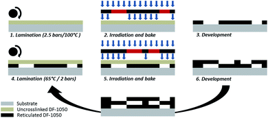 | ||
| Fig. 1 Schematic 3D fabrication process with the superposition of DF-1000 series and the use of lamination and lithography techniques. | ||
First, the dry film was laminated onto a planar substrate (silicon, glass or a flexible carrier substrate depending on the targeted application). Then the DF-1000 layer was exposed to UV-light baked at 100 °C and lastly developed in a bath of cyclohexanone. The next layer was then stacked onto the first one by lamination and the process performed as previously. These steps can be then repeated as much as necessary in order to complete the multilevel device.
Stress measurement
To study the remaining stress of the materials, we used a mechanical profilometer (KLA-Tencor P-16+) and the calculation of residual stress was done directly by the software of the apparatus from the Stoney equation:15where Es and νs are the Young's modulus and the Poisson coefficient of the substrate respectively, R the curvature radius and t the thickness (s and f refer respectively to the substrate and the film).
UV-visible and fluorescence spectroscopies
We used a UV-visible spectrophotometer (190–820 nm) Hewlett Packard HP8452A diode array to study the absorption of the photoresist. Measurements are obtained in transmission.To quantify the autofluorescence of the studied polymer we used a PTI (Photon Technology International) Quantamaster 1. Samples were placed at 45° from the incident beam. The resistance to pressure and solvents of devices was tested by imaging microchannels with a fluorescence microscope (Olympus BX51) at 470 nm excitation wavelength.
Solvent resistance
We tested the resistance to four solvents commonly used in microfluidic devices: ethanol, isopropanol, acetone and dimethyl sulfoxide (DMSO). This was done by immersing the sample (50 μm thick layer laminated onto a silicon substrate) into the different solutions and by studying the aspect of the film surface with optical microscopy. The film thickness was also checked with a mechanical profilometer.Results and discussion
DF-1050 is a negative dry film photoresist manufactured by Engineered Materials Systems, Inc. The DF-1000 series is available in a broad range of thicknesses between 5 and 50 μm (the last two numbers of 1000 indicate the thickness of the dry film). It is sold in roll package and contained between two liners which can be easily removed. The material is composed of oxirane, 2,2′-[1,6-naphthalenediylbis(oxymethylene)]bis-(25–35%) and antimony compounds (5–10%). The rest is trade secret.Resolution and microchannel fabrication with DF-1000 series
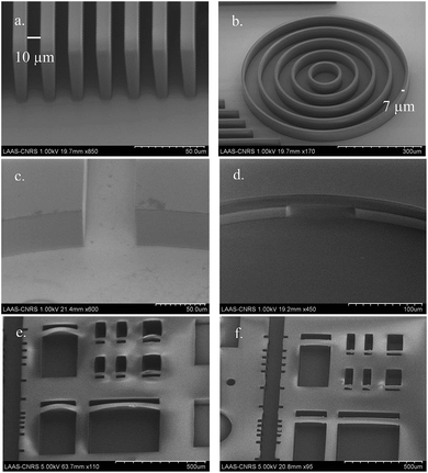
Because the dimension of microchannels can be significantly varied on a single chip we first studied the resolution of this photoresist on a single layer of 50 μm thickness. To ensure the adhesion of the layer onto the substrate, the lamination was done at 100 °C with rollers speed and pressure of 0.5 m min−1 and 2.5 bars respectively. The protection liner was removed immediately after lamination prior to the photolithography step.In order to optimize the patterns resolution and aspect ratio we studied several exposure doses at 365 nm and post exposure bake (PEB) times at 100 °C. Fig. 2a and b shows examples of achieved results.
In Fig. 2a 10 μm wide and 50 μm high opened structures are showed and in Fig. 2b free standing structures of 7 μm width and 50 μm height are visible (below 7 μm width the structures collapse). DF-1050 dry film enabled an aspect ratio of 7![[thin space (1/6-em)]](https://www.rsc.org/images/entities/char_2009.gif) :
:![[thin space (1/6-em)]](https://www.rsc.org/images/entities/char_2009.gif) 1 for free standing structures and 5
1 for free standing structures and 5![[thin space (1/6-em)]](https://www.rsc.org/images/entities/char_2009.gif) :
:![[thin space (1/6-em)]](https://www.rsc.org/images/entities/char_2009.gif) 1 for channel structures. However, as illustrated in Fig. 2a the sidewalls profile is slightly negative. Nevertheless the angle is estimated to 92°.
1 for channel structures. However, as illustrated in Fig. 2a the sidewalls profile is slightly negative. Nevertheless the angle is estimated to 92°.
To study the compatibility of DF-1000 series with microfluidic application we manufactured various microchannel designs by combining lamination and photolithography techniques as described before. Previous works on homemade SU-8 dry film photoresist9,16 helped us to determine the best lamination parameters (speed, temperature and pressure) for the upper layers. To avoid collapse of the upper layer in the lower layer, the lamination temperature had to be lowered but was maintained high enough to ensure the adhesion between the two layers. We determined that, to laminate an uncrosslinked layer of DF-1000 series onto a reticulated and structured one, the optimal temperature was 65 °C with rollers speed and pressure of 1 m min−1 and 2 bars respectively. Fig. 2c and d illustrate an example of microchannels fabricated following this protocol.
After exposure, the photoresist was baked to catalyze the polymerization reaction (PEB). However, when using a regular hot plate we observed a deformation of the upper layer as shown in Fig. 2e. This was confirmed by mechanical profilometer measurement. This phenomenon may be due to the residual stress of the material or the presence of air trapped in open microstructures after the lamination of the upper layer. During the bake, air pressure in microchannels increased faster than the cationic polymerization of the materials. So the material was deformed before reaching the mechanical stiffness sufficient to resist to the increase of air pressure. To minimize this swelling a hot plate with a thermal ramp bake was used (Delta 6 HCP/BM from Suss MicroTec). The start temperature was 65 °C. It was then ramped up to 100 °C (10 °C min−1) and down to 25 °C (5 °C min−1). Fig. 2f shows the benefit of ramped bake: the deformation is still there but significantly reduced.
Residual stress measurement
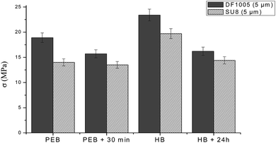
3D microfluidic devices fabrication implies to stack several layers. Therefore residual mechanical stress σ of the material may be a major issue and has to be controlled carefully. For example, a high level of stress can generate cracks in the layer or can make the alignment step very difficult because of the bending of the wafer. Although the residual stress of the SU-8 is not negligible, the manufacturing of 3D chips with this photoresist has already been demonstrated and widely used.9,16 So we measured and compared the stress value of non-structured but cross-linked layers of DF-1005 with those measured in SU-8 (5 μm thickness each). According to the manufacturer, a hard bake (HB) is recommended to improve the chemical resistance of the materials to aggressive solvents. So we studied the variation of the residual stress directly after PEB and HB and its evolution through time. For the DF-1005 the PEB was performed on a hot-plate at 100 °C for 5 min and the HB in an oven at 175 °C for 1 h. Regarding the SU-8 the PEB was done on a hot-plate at 95 °C for 3 min and the HB at 125 °C for 2 min. Results are given in Fig. 3.We observed that the stress is tensile and that immediately after PEB it was higher for the DF-1005 than for the SU-8. However, a relaxation occurred rapidly following the PEB step and the stress value decreased from 19 to 16 MPa after 30 min. We noticed that the stress of the SU-8 underwent no significant variation in the same time and that the final values of stress in DF-1005 and SU-8 were close to each other.
In both cases the HB caused a strong increase of the stress level of the layer. This evolution was mainly due to the increase of the reticulation level. Nevertheless a relaxation was visible and stable after 24 h for both materials and stabilized around 15 MPa, in the same order of magnitude than after PEB.
This study showed that residual stress in DF-1000 series film is comparable to SU-8 one even if it is 12% higher. This result appeared encouraging and suggested that multi-level structures could be realized. As a matter of fact, as it will be demonstrated thereafter we have successfully fabricated 3D microfluidic devices composed of five layers of dry film.
Compatibility of DF-1050 with fluorescence observation
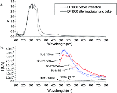
In many microfluidics applications fluorescence imaging is a privileged technique for device characterization and biological detection. Very often, molecular fluorophores or fluorescent particles are used as tracers in fluids or attached to the species of interest (DNA, proteins, cells, etc.,…). Therefore, it is a prerequisite that the material used to fabricate microchannels is compatible with fluorescence observation and more precisely with a wide variety of fluorescent dyes (see Table 2 in ESI†).These values must be compared to the DF-1050 absorption spectrum presented in Fig. 4a. Most dyes absorb and re-emit above 490 nm in a region where absorption in DF-1050 is weak and can be considered as negligible with regards to the fluorescence intensity commonly obtained with those dyes.
Another aspect which has to be taken into account is the natural auto-fluorescence of the film. As can be deduced in Fig. 4a the film remained colored after complete processing. As it could be an issue for fluorescence based experiments, we characterized and confronted the autofluorescence of three reticulated materials: DF-1050, SU-8 and PDMS. We studied their responses at 470 and 545 nm (5 nm spectral bandpass). The detector was set to record emission signal at 475 and 550 nm to 800 nm (increments of 1 nm).
According to Fig. 4b fluorescence intensity of SU-8 and DF-1050 were quite similar for the both excitation wavelengths but however higher than with PDMS which is not fluorescent according to this experimentation (detection limit of the apparatus) and Piruska et al.17
The autofluorescence of the SU-8 did not interfere in the fluorescence detection.18
These experiments show that DF-1000 series have a low autofluorescence and are therefore compatible with most of microfluidic applications using fluorescence detection.
Solvent resistance
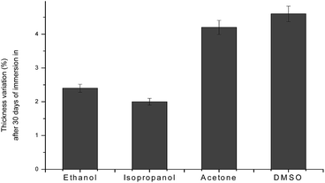
Various liquids are used in microfluidics chips including some aggressive solvents like acetone or dimethyl sulfoxide. It was thus of prime importance to check the resistance of DF-1050 to these solvents. So we immersed for 30 days reticulated and hard baked layers of DF-1050 into four solvents (ethanol, isopropanol, acetone and dimethylsulfoxide). We characterized the thickness with a mechanical profilometer. Results on thickness variation are presented in Fig. 5.After 30 days of immersion the maximum thickness variation observed with DMSO is less than 5%. Moreover, observation with an optical microscope of the surface showed no cracks.
We also tested the adhesion of two layers including 2D microchannels to different solvents (ethanol, isopropanol and acetone) at various pressures with a MFCS TM 7 bars from Fluigent. The adhesion of two layers is alcohol and acetone resistant (no visible liquids outside the microchannels) and no delamination occurred up to 3.5 bars fluid pressure.
These studies evidenced that dry film DF-1000 series was chemically resistant to aggressive solvents and that the bonding between layers was not affected by solvent effect. It has to be highlighted that this chemical resistance makes DF films compatible with a large set of microfabrication processes as lift-off lithography, metal deposition and etching, etc.,…
Biocompatibility
In a first approach, we studied qualitatively the toxicity of the dry film to cells. After 24 h in contact with the materials, we observed that the cells were still clinging in the surface of the material. We also subcontracted a quantitative study to NAMSA®, a company specialized in medical regulatory services. Details of this study are given in ESI.†Fast manufacturing of complex three dimensional microfluidic mixers
In microfluidics, 3D structures can be useful for a tremendous amount of applications, and a specific field where we can see the relevancy of this technique is micromixing. Various designs were reviewed regarding micromixers,19 and the particular case of the Baker's transformation has been thoroughly described. Carriere,20 in 2007, suggested (using FEM simulations techniques) a genuine, new 3D design to perform this transformation in a microfluidic device. A similar design was first realized in 2012 by Liao et al.,21 using femtosecond laser writing which is a non-conventional microfabrication technique. However, with our dry film lamination protocol, we built such a micromixer with a low cost and simple method, and showed the device was clearly functional.Four levels of dry film were necessary just to build the structure (see Fig. 6a), and we chose to add a “floor” layer so in order to keep identical wettability properties on the four walls (it is possible to have glass substrate in contact with the fluid, but it was not desired in that case). The “roof” layer allowed closing the channels and creating the inlets and outlets holes. This makes a total of 5 levels of film to laminate and 4 photolithography steps. The total time to fabricate such a device was estimated to 5 h 15 including surface treatment, lamination, insolation, post exposure bake and development steps.
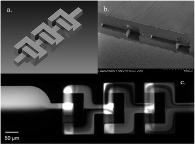 | ||
| Fig. 6 (a) Design and (b) SEM image of cross section of the 3D microfluidic mixer.20 (c) Fluorescence microscopy image of the 3D micromixer for a 470 nm excitation wavelength (the two fluids are water and fluorescein in water). The flow rate is 40 μL min−1. | ||
The micromixer pattern was formed of 3 loops, and this “mixing unit” was repeated 10 times in the same device. The width of the channels was 45 μm, and the height was imposed by the film thickness (20 μm for this device). To observe a cross section of the three-dimensional microchannels network the device was cut lengthwise with a diamond saw. Fig. 6b shows a SEM picture of the mixing device.
A homemade Teflon and aluminum chip holder was manufactured to place the chip and to ensure fluidic connections. The 15 × 20 mm2 chip can fit two independent mixing devices (total of 4 inlets and 2 outlets). The solutions were injected thanks to UpChurch 10–32 coned nuts and ferrules, as well as Teflon tubing (1/16′′ O.D. 0.3 mm I.D.).
Flow control was performed with 1 mL SGE glass syringes and a Cetoni Nemesys syringe pump. All the solutions (D.I. water, and fluorescein in water at a concentration of 0.6 mmol L−1) have been filtered (0.22 μm filters) prior to their use.
Efficient mixing was observed at very low Reynolds numbers. The same flow rate was applied for water and fluorescein solution. In Fig. 6c, we can see the first pattern (3 loops) of the device: we observe that the fluorescein concentration field is divided in 2, 4, and 8 values before the inlet of the 1st, 2nd and 3rd loops respectively, which matches the expected results of the baker's transformation. After the 3rd loop, diffusion is such as we cannot distinguish all of the 16 different levels of concentration we would have with a non-diffusive transformation.
By applying a flow rate of 40 μL min−1 (Re ≈ 15, Pe ≈ 3.1), a homogeneous solution was obtained after about 15 loops, showing we can achieve mixing with a low Reynolds number, even with quite small contribution from diffusion.
Those results proved that our lamination technology enables realization of operational complex 3D structures, with original microfluidic functions involving 3D flows management.
Conclusions
Using a commercially dry film photoresist DF-1000 series to build low cost 3D microfluidic devices with lamination and UV-lithography techniques was demonstrated and investigated in different ways essential in microfluidic area.The material is able to perform high aspect ratio of 7![[thin space (1/6-em)]](https://www.rsc.org/images/entities/char_2009.gif) :
:![[thin space (1/6-em)]](https://www.rsc.org/images/entities/char_2009.gif) 1 for free standing structures and 5
1 for free standing structures and 5![[thin space (1/6-em)]](https://www.rsc.org/images/entities/char_2009.gif) :
:![[thin space (1/6-em)]](https://www.rsc.org/images/entities/char_2009.gif) 1 for channel structures. The deformation of the upper layer during the post exposure bake on a classical hotplate was studied and a protocol with a ramp bake hotplate was established to minimize this phenomenon. We characterized the residual stress of the dry film after each bake and showed that it was in the same order of magnitude that SU-8 photoresist. We proved the chemical stability of this dry film photoresist to the common organic solvents. We showed that the material had a low autofluorescence similar to the SU-8 photoresist and a low absorption in the visible region after irradiation and bake. However, through different fluorescence experiments we demonstrated the compatibility of this material with most fluorescence based experiments. We also proved its biocompatibility which makes it suitable for biological applications.
1 for channel structures. The deformation of the upper layer during the post exposure bake on a classical hotplate was studied and a protocol with a ramp bake hotplate was established to minimize this phenomenon. We characterized the residual stress of the dry film after each bake and showed that it was in the same order of magnitude that SU-8 photoresist. We proved the chemical stability of this dry film photoresist to the common organic solvents. We showed that the material had a low autofluorescence similar to the SU-8 photoresist and a low absorption in the visible region after irradiation and bake. However, through different fluorescence experiments we demonstrated the compatibility of this material with most fluorescence based experiments. We also proved its biocompatibility which makes it suitable for biological applications.
Lastly, a complex 3D micromixer structure was studied. This structure which was conceived in 2007 remained unrealized until 2012 due to the lack of technology enabling its manufacturability. Thanks to DF films, we proved that building such a device became possible with low cost and easy-going technologies. By this way, all the criteria for microfluidic use were checked. Through these investigations we demonstrated the potentiality of this material to implement innovative microfluidic functions in 3D microchannels network.
Acknowledgements
This work was supported by the PIA – Nanobiotechnology project Digidiag, the National Defence Agency (DGA) and was partially realized in the clean room of LAAS-CNRS member of the French RENATECH network.Notes and references
- G. M. Whitesides, Nature, 2006, 442, 368 CrossRef CAS PubMed.
- A. Manz, N. Graber and H. M. Widmer, Sens. Actuators, B, 1990, 1, 244 CrossRef CAS.
- D. C. Duffy, J. C. McDonald, O. J. A. Schueller and G. M. Whitesides, Anal. Chem., 1998, 70, 4974–4984 CrossRef CAS PubMed.
- L. Martynova, L. E. Locascio, M. Gaitan, G. W. Kramer, R. G. Christensen and W. A. MacCrehan, Anal. Chem., 1997, 69, 4783–4789 CrossRef CAS.
- J. S. Rossier, M. A. Roberts, R. Ferrigno and H. H. Girault, Anal. Chem., 1999, 71, 4294–4299 CrossRef CAS PubMed.
- P. Abgrall, L. N. Low and N. T. Nguyen, Lab Chip, 2007, 7, 520–522 RSC.
- J. D. Gelorme, R. J. Cox and S. A. R. Gutierrez, US Pat. no. 4882245, 1989.
- K. Y. Lee, N. LaBianca, S. A. Rishton, S. Zolgharnain, J. D. Gelorme, J. Shaw and T. H. P. Chang, J. Vac. Sci. Technol., B: Microelectron. Nanometer Struct. Process., Meas., Phenom., 1995, 13, 3012–3016 CrossRef CAS.
- P. Abgrall, C. Lattes, V. Conédéra, X. Dollat, S. Colin and A. M. Gué, J. Micromech. Microeng., 2006, 16, 113–121 CrossRef.
- P. Vulto, N. Glade, L. Altomare, J. Bablet, L. D. Tin, G. Medoro, I. Chartier, N. Manaresi, M. Tartagni and R. Guerrieri, Lab Chip, 2005, 5, 158–162 RSC.
- R. C. Meier, V. Badilita, J. Brunne, U. Wallrabe and J. G. Korvink, Biomicrofluidics, 2011, 5, 034111 CrossRef PubMed.
- U. Stöhr, P. Vulto, P. Hoppe, G. Urban and H. Reinecke, J. Micro/Nanolithogr., MEMS, MOEMS, 2008, 7, 033009 CrossRef PubMed.
- K. Kalkandjiev, L. Riegger, D. Kosse, M. Welsche, L. Gutzweiler, R. Zengerle and P. Koltay, J. Micromech. Microeng., 2011, 21, 025008 CrossRef.
- N. Wangler, L. Gutzweiler, K. Kalkandjiev, C. Müller, F. Mayenfels, H. Reinecke, R. Zengerle and N. Paust, J. Micromech. Microeng., 2011, 21, 095009 CrossRef.
- G. G. Stoney, Proc. R. Soc. London, Ser. A, 1909, 82, 172–175 CrossRef CAS.
- R. Fulcrand, D. Jugieu, C. Escriba, A. Bancaud, D. Bourrier, A. Boukabache and A. M. Gué, J. Micromech. Microeng., 2009, 19, 105019 CrossRef.
- A. Piruska, I. Nikcevic, S. H. Lee, C. Ahn, W. R. Heineman, P. A. Limbach and C. J. Seliskar, Lab Chip, 2005, 5, 1348–1354 RSC.
- S. Cargou, H. Kabbara, M. Mader, P. Joseph, A. Boukabache and A. M. Gué, European Conference on Microfluidics μFLU12-135, 2012, p. 7 Search PubMed.
- C.-Y. Lee, C.-L. Chang, Y.-N. Wang and L.-M. Fu, Int. J. Mol. Sci., 2011, 12, 3263–3287 CrossRef CAS PubMed.
- P. Carriere, Phys. Fluids, 2007, 19, 118110 CrossRef PubMed.
- Y. Liao, J. Song, E. Li, Y. Luo, Y. Shen, D. Chen and K. Midorikawa, Lab Chip, 2012, 12, 746–749 RSC.
Footnote |
| † Electronic supplementary information (ESI) available. See DOI: 10.1039/c4ra09097g |
| This journal is © The Royal Society of Chemistry 2014 |


