Oxygen-induced abnormal photoelectric behavior of a MoO3/graphene heterocomposite

Juehan Yanga, Renxiong Lia, Nengjie Huoa, Wen-Long Maa, Fangyuan Lua, Chao Fana, Shengxue Yanga, Zhongming Wei*b, Jingbo Li*a and Shu-Shen Lia
aState Key Laboratory for Superlattices and Microstructures, Institute of Semiconductors, Chinese Academy of Sciences, P.O. Box 912, Beijing 100083, China. E-mail: jbli@semi.ac.cn
bNano-Science Center & Department of Chemistry, University of Copenhagen, Universitetsparken 5, DK-2100 Copenhagen Ø, Denmark. E-mail: zmwei@semi.ac.cn

Received 12th August 2014 , Accepted 24th September 2014

First published on 24th September 2014


Abstract

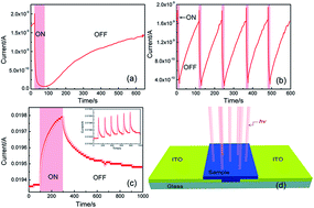
A MoO3 nanoflakes/graphene heterocomposite synthesized by a water bath method showed unusual photoelectric behavior. Its resistance increased under visible light irradiation in air. The behavior arises from the physical contact between the two materials, which leads to hole doping in graphene. Thus, the increase of electrons in the MoO3 nanoflakes induced by desorption of oxygen molecules from its surface under visible light was probably the main reason for the change in resistance. This was confirmed by the resistance of the heterocomposite in a vacuum being 102 times larger than that in air, and by the photoelectric measurements under Ar. The MoO3 nanoflakes/graphene heterocomposite exhibits great potential for use in oxygen gas sensing.


Introduction

Graphene has attracted great attention in the past decade due to its remarkable properties, such as high carrier mobility, wavelength independent light absorption and ultra-highspeed photoresponse.1,2 These unique properties make graphene suitable for many applications in various fields, including field effect transistors,3 photodetectors,4 solar cells,5 supercapacitors,6 and transparent electrodes for electronic devices.7 Furthermore, many graphene derivatives have been studied recently to improve its performance. One of the most important derivatives is graphene oxide which has already been used in centimeter-scale flexible and transparent electrodes,8 antibacterilas9 and chemiluminescence.10 Other derivatives, such as graphene quantum dot-like arrays, have been used in photodetectors and exhibited a high photoresponse from the visible to the mid-infrared region.4 In addition to these single-component derivatives, graphene-based composites or hybrids also show novel attractive properties in many fields. For example, graphene-PbS quantum dot hybrids phototransistors displayed ultrahigh photoconductive gain.11 Graphene/amorphous carbon films exhibited high performance in photovoltaic applications.12 The improved properties of the graphene-based composite/hybrids mostly arise from the interface interaction between graphene and the other material. In order to improve and understand graphene-based electronic and photoelectronic devices, it is important to investigate the interface interaction with other materials.

Recently, easily synthesized metal oxide nanostructures which exhibit many outstanding properties have been reported13–15 and used to tune the properties of other materials by interface interactions. For example, TiO2 was used to induce photocurrents in both p-type and n-type organic thin film transistors under UV light in the opposite direction,16 and induce a significant UV and visible light photoresponse in graphene.17 The ZnO nanorod/graphene composite showed an increase in UV light sensitivity.18

Based on this background, the interface reactions between graphene and metal oxides are crucial for graphene-based heterocomposites/hybrids and the related electronic devices and must be investigated thoroughly. Herein, we used a facile water bath method to synthesize the MoO3 nanoflakes/graphene heterocomposite. The large work function difference between MoO3 and graphene caused hole doping in graphene. During the photoresponse measurements, oxygen-assisted charge transfer between the MoO3 nanoflakes and graphene caused an abnormal increase in the resistance of the heterocomposite under visible light. This showed that the interface interaction between graphene and metal oxide nanostructures could be strongly influenced by photodesorption of gas molecules like oxygen. This unusual photoelectric behavior could be used to bridge the gap between photodetectors and gas sensors. In addition, the high O2 sensitivity of the MoO3 nanoflakes/graphene heterocomposite shows great potential for use as an O2 gas sensor.

Experimental

Synthetic method

Commercial graphene (2–6 layers, n-type), which was made by the arc discharge method, was purchased from Beijing Tsing Da Ji Guang Technology Development Co., Ltd. The other chemical reagents were all bought from Sinopharm Chemical Reagent Co., Ltd.

Ammonium heptamolybdenum tetrahydrate (0.9 g) was dissolved in distilled water (10 mL), and then 4.5 mol L−1 nitric acid was added to the solution dropwise (10 × 50 μL drops) and stirred for 20 min. Graphene (0.05 g) was added to the solution and stirred vigorously for 2 h at room temperature. The solution was then heated in hot water at 65 °C for 180 min under continuous stirring. After the mixture was allowed to cool to room temperature, the grey precipitate was collected, washed several times with distilled water, centrifuged, and dried for 6 h at 80 °C. The crude MoO3 nanoflakes/graphene heterocomposite was then annealed at 400 °C in N2 gas flow for 30 min.

To exclude the effect of nitric acid on graphene, 10 drops (50 μL each) of 4.5 mol L−1 nitric acid were added to distilled water (10 mL). Graphene (0.05 g) was added to the solution under and stirred vigorously for 2 h at room temperature and 3 h at 65 °C. The graphene was collected, washed several times with distilled water, centrifuged, and dried for 6 h at 80 °C.

The procedure for synthesizing the MoO3 nanoflakes was the same as that for the MoO3 nanoflakes/graphene heterocomposite although no graphene was added to the mixture.

Characterization

The as-prepared sample was analyzed by scanning electron microscopy (SEM) and Raman spectroscopy, measured by a Renishaw Raman system with laser wavelength of 514 nm.

Device fabrication and photoresponse measurements

Two indium tin oxide (ITO) glass electrodes were separated by a nonconducting gap. The as-synthesized MoO3 nanoflakes/graphene heterocomposite were dispersed in ethanol, then dropped onto the surface of the gap between the two electrodes, and dried naturally at room temperature. This led to a thin film of the as-synthesized MoO3 nanoflakes/graphene heterocomposite forming and covering the gap between the two ITO electrodes. A red laser with a wavelength of 650 nm and power of 50 mW cm−1 was used as a light source. A CHI 660 electrochemical apparatus was used to measure the current flowing through the sample under a voltage of 10 V, which was applied across the ITO–ITO electrode pairs, under or without irradiation from the red laser.

Results and discussion

Morphology

The morphology of the MoO3 nanoflakes/graphene heterocomposite is shown in Fig. 1. The MoO3 nanoflakes were rectangular. Their average length was 20–25 μm, and the average width was 3–5 μm. The graphene exhibited a curled morphology and tended to aggregate. The graphene aggregates dispersed in the MoO3 nanoflakes and came into physical contact with the nanoflakes.
image file: c4ra08557d-f1.tif
Fig. 1 (a)–(d) SEM images of the MoO3 nanoflakes/graphene heterocomposite.

The X-ray diffraction (XRD), X-ray photoelectron spectra (XPS) and thermo-gravimetric analysis (TGA) results are shown in the ESI.

Raman spectra

The Raman spectra of the MoO3 nanoflakes/graphene heterocomposite, the as-synthesized MoO3 nanoflakes and the graphene precursors are shown in Fig. 2. No peak shift was found for the MoO3 in the MoO3 nanoflakes/graphene heterocomposite by comparing the curves for the heterocomposite and the as-synthesized MoO3 nanoflakes (Fig. 2(a)). In addition, the peaks at 243, 284, 336, 374, 665, 820 and 994 cm−1 of the MoO3 nanoflakes/graphene heterocomposite curve and MoO3 nanoflakes curve fit well with the structure of MoO3 reported in ref. 19. All peaks of the two curves were sharp and had high intensity, which indicated that the crystallinity of both the MoO3 nanoflakes in the heterocomposite and the as-synthesized MoO3 nanoflakes was good. In addition, graphene had no significant effect on the formation of MoO3 nanoflakes during the synthesis of the heterocomposite.
image file: c4ra08557d-f2.tif
Fig. 2 Raman spectra of the MoO3 nanoflakes/graphene heterocomposite, the as-synthesized MoO3 nanoflakes (a) and the graphene precursors (b).

In Fig. 2(b), the two curves which corresponded to the graphene precursor and the graphene in heterocomposite had the same G peak at 1583 cm−1 and 2D peak at 2704 cm−1.20 However, the D peak of graphene at 1350 cm−1 moved to 1370 cm−1, and the intensity ratio of the D peak to G peak increased after the formation of the heterocomposite.

Photoelectric property measurements

Fig. 3(a) and (b) show the photoelectric properties of the MoO3 nanoflakes/graphene heterocomposite and the graphene that was used to synthesize the heterocomposite.
image file: c4ra08557d-f3.tif
Fig. 3 (a) and (b) Photoresponse of the MoO3 nanoflakes/graphene heterocomposite in air, (c) photoresponse of graphene in air and (d) schematic of the photoresponsive device.

In Fig. 3(a), the current flowing through the sample (for the device fabrication method see Experimental section) was reduced to 10% of its original value when it was irradiated with red light (λ = 650 nm). The current recovered to its original value when it was not irradiated. This means the resistance of the as-synthesized MoO3 nanoflakes/graphene heterocomposite was increased by about 10 times by irradiation with red light. Furthermore, it took about 10 s for the current to decline to its minimum value (10% of the current before irradiation), and took more than 500 s to reach its original value, which indicated that the recovery of the original resistance was much more difficult than the increase in resistance. In Fig. 3(b), the pink areas represent the periods of irradiation, showing that the increase and decrease in resistance can be repeated well with the on/off cycles of the red light irradiation, which indicates the good repeatability and stability of the device. In addition, the resistance recovery process took a longer time in the on/off cycle.

However, the current flow through the pure graphene increased under visible light irradiation, as shown in Fig. 3(c), and it took about 200 s to reach its saturation value (increase of about 2%) and slowly recovered to its original value after the irradiation was off. Therefore, the resistance of graphene decreased under visible light irradiation, implying that the photoelectric behavior of the graphene is the opposite of that of the heterocomposite. Lin et al. reported that SnO2 and Pd-doped SnO2 nanoparticles also exhibit similar behavior under UV light.21

Electrons in the valence band of semiconductors can absorb numerous photons and be excited into the conduction band if the photon energy is larger than their band gap energy. Thus, the amount of conducting carriers in semiconductors increases upon light irradiation, decreasing the resistance of semiconductors. As a large band gap semiconductor, MoO3 has a large band gap of about 3.1 eV;22 therefore, UV light with a wavelength of <400 nm should be required to excite the electron–hole pairs in MoO3. However, the MoO3/graphene heterocomposite showed a photoresponse to red light (λ = 650 nm) which did not have enough energy to excite electron–hole pairs in MoO3. In addition, the resistance of the MoO3/graphene heterocomposite increased under red light irradiation, which is the opposite behavior to conventional semiconductors, in which resistance decreases under light irradiation. Furthermore, for the graphene, which was one constituent of the heterocomposite, the resistance decreased under irradiation with the same red light source. Thus, the unusual photoelectric behavior of the MoO3/graphene heterocomposite was did not arise from the properties of the individual constituents of the heterocomposite and resulted from the strong interaction at the interface between MoO3 and graphene in the heterocomposite.

To investigate the origin of the photoelectric behavior further, two control experiments were carried out. First, the photoelectric properties of the MoO3/graphene heterocomposite were measured in an Ar atmosphere. The sample was placed in a chamber that was then filled with Ar gas for more than 20 min to exclude air, creating an oxygen-free or low-oxygen environment for the photoelectric measurements. The results are shown in Fig. 4(a). Although the current still declined, indicating that the resistance of the heterocomposite still increased under light irradiation in an Ar atmosphere, the current decreased by only about 15%,which is much smaller than the decrease of 90% in air. This means that under visible light irradiation the increase in resistance of the heterocomposite in Ar (about 1.33 times) was much less than that in air (about 10 times). Thus, the light irradiation increased the heterocomposite resistance in air and Ar, and the inert gas atmosphere decreased the unusual photocurrent response.


image file: c4ra08557d-f4.tif
Fig. 4 (a) Current of the MoO3/graphene heterocomposite sample in an Ar atmosphere under light irradiation (pink areas) and with outlight irradiation (white areas) and (b)current flowing through the heterocomposite sample during the pumping process (pink areas) and in an air atmosphere (white areas).

In addition, the current measured in Ar shown in Fig. 4(a) was 100 times smaller than that in air (Fig. 3(a) and (b)), indicating that the resistance of the heterocomposite in Ar was about 100 times bigger than that in air. Therefore, the inert gas atmosphere also can increase the resistance of the heterocomposite. Futhermore, based on our experimental results, the longer the chamber is filled with Ar gas the larger the heterocomposite resistance should be; however, a smaller increase in resistance (or current decrease) of the MoO3/graphene heterocomposite was induced by visible light irradiation. Thus, air was not the only factor that influenced the resistance of the heterocomposite, although it was the key factor that determined the abnormal photoresponse. Therefore, the abnormal photoelectric behavior was probably associated with the O2 in the air and the interface interaction between O2 and the heterocomposite.

In order to investigate the role of O2 molecules, another control experiment was done in a vacuum chamber. Because the device current was below the detection limit of our measurement system when the vacuum was very high, the chamber was pumped for only 100 s for each cycle to investigate the effect of O2 molecules on the heterocomposite. In Fig. 4(b), the pink areas represent the periods under vacuum (during pumping). The current immediately decreased at the beginning of pumping, and showed a dramatic decrease during pumping and an increase when pumping stopped. However, compared with the rapid decrease in current during pumping, the current immediately recovered to a value and then slowly increased to its original value when the pumping stopped and the chamber filled with air. This means that a vacuum can also increase the resistance of the heterocomposite, similar to visible light irradiation. The curve also showed that the decrease and increase of the current could be repeated and followed the on/off cycle of the vacuum closely. Surprisingly, the current of the device in air was higher than that in a vacuum by more than 102 times. Based on the fast, reproducible response of the device, the heterocomposite was highly sensitive to O2 at room temperature.

Previous work has reported that MoO3 is sensitive to O2,23 although high operating temperatures above 200 °C were required. In addition, the resistance of the nitric acid-treated graphene showed a decrease during pumping, as shown in Fig. 5, which excludes the effect of the graphene. Thus, the decrease of the heterocomposite resistance during pumping is mostly derived from the interface interaction between the two components (MoO3 and graphene) involving O2. It was also reported that O2 molecules can be adsorbed on the surface of semiconductors, including metal oxides like TiO2,24 and the surface vacancy on samples can increase the O2 adsorption.17 The adsorbed O2 molecules can readily trap the electrons from semiconductors by forming O2 anions on their surface.24 Furthermore, the adsorbed O2 molecules can desorb under visible light irradiation and release the trapped electrons.17,25 This means that even though only UV light can excite electron–hole pairs in MoO3, visible light still can change the carrier density of MoO3 through the O2 molecules adsorbed on the surface.


image file: c4ra08557d-f5.tif
Fig. 5 Current of the HNO3-treated graphene during pumping (pink areas) and in an air atmosphere (white areas).

The mechanism that causes the unusual photoelectric behavior of the heterocomposite could be explained as follows. The large difference in work function (>2 eV) between graphene26,27 and MoO3 (ref. 28) means that physical contact between graphene and MoO3 can inject electrons from graphene to MoO3 to align the Fermi levels of the two materials.29 The electron injection process is shown in Fig. 6(a) and (b). The electron injection creates hole doping in graphene, resulting in the change from n-type to p-type graphene (Fig. 6(c)).29


image file: c4ra08557d-f6.tif
Fig. 6 Charge transfer mechanism between MoO3 nanoflakes and the graphene in the heterocomposite. (a) The large work function difference (b) causes graphene electrons to be injected into the MoO3 nanoflakes resulting in (c) hole doping in graphene. (d) The adsorbed O2 molecules desorbed under visible light irradiation release trapped electrons back to MoO3 nanoflakes. (e) The Fermi level of MoO3 nanoflakes moves up from its original position (black dotted line) to a new higher position (red dotted line), making the Fermi level of MoO3 nanoflakes higher than the graphene Fermi level allowing the MoO3 nanoflake electrons to be injected into graphene. (e) Some O2 molecules desorb from the surface of the MoO3 nanoflakes when the heterocomposite is not irradiated, and the trapped MoO3 nanoflake electrons shift the Fermi level of the MoO3 nanoflakes down from its original position (red dotted line) to a lower new position (black dotted line). (f) To align the Fermi level, the Fermi level of graphene moves down from its original position (red dotted line) to a lower new position (black dotted line).

Under visible light irradiation, some of the adsorbed O2 molecules desorb from the surface of the MoO3 nanoflakes and release the electrons back to the MoO3 nanoflakes.17 Thus, the carrier density of the MoO3 nanoflakes increases and the equilibrium between the MoO3 nanoflakes and graphene Fermi level is broken. This results in some of the released electrons being injected into the graphene, and then recombining with the graphene holes.17 Some of the released electrons behave like Coulomb traps at the MoO3 nanoflakes/graphene interface, quenching the graphene holes and lowering the hole mobility (Fig. 6(d)).24 Therefore, desorption of O2 molecules from the surface of the MoO3 nanoflakes could decrease the transport in graphene. Furthermore, although the desorption of O2 molecules may increase the carrier density of the MoO3 nanoflakes (not all the released electrons are injected into the graphene or act as a Coulomb trap), which could enhance the transport of the MoO3 nanoflakes within limits, the high carrier mobility of graphene1 means that the decrease in the transport of graphene dominates the change in transport of the whole heterocomposite system. Thus, the resistance of the heterocomposite increases under visible light irradiation, which results in the decreased current. In addition, in a vacuum, almost all of the adsorbed O2 molecules desorb, which explains why the resistance of the heterocomposite was 102 times larger in a vacuum than in air. When the photoelectric properties were measured in Ar, the number of adsorbed O2 molecules on the surface of MoO3 nanoflakes was far lower than that in air. Therefore, fewer O2 molecules were desorbed from surface of MoO3 when the heterocomposite was irradiated with visible light. Thus, the decrease in current under visible light irradiation in Ar was much smaller than that in air (see Fig. 4(a)).

Based on our experiment data, visible light irradiation is a simple, convenient approach to desorb O2 molecules. In contrast, when the light was off, some O2 molecules are readsorbed on the surface and trap the MoO3 nanoflake electrons to form anions. This decreases the number of electrons in the MoO3 nanoflakes and shifts the Fermi level of the MoO3 nanoflakes down (Fig. 6(e)). To align the Fermi level of MoO3 nanoflakes and graphene, the Fermi level of the graphene also moves down, which increases the number of hole carriers in the graphene, as shown in Fig. 6(f). In addition, the decrease of electrons in MoO3 nanoflakes decreases the number of charge traps, increasing the hole mobility in graphene. Therefore, the current flowing through the sample increased when it was not irradiated with visible light. The recovery of the current took longer than the decrease in current, which indicated that the adsorption of the oxygen molecules was more difficult than the desorption. In addition, as shown in Fig. 3(a) and (b), the current increased quickly at first and then decreased under visible light irradiation. The reason for this behavior may be that when the heterocomposite was irradiated, the graphene absorbed the light energy and generated hole–electron pairs, which decreased the resistance of the graphene (Fig. 3(c)). Thus, the resistance of the MoO3/graphene heterocomposite system decreased during the first period of irradiation, which initially led to the quick increase in current. Subsequently, more oxygen molecules were desorbed from the surface of the MoO3 nanoflakes, accompanied by the release of the trapped electrons. The released electrons injected into graphene and recombined with the graphene holes. According to our proposed mechanism, the resistance of the heterocomposite would increase. Similar observations have been reported in ref. 30.

Conclusions

A MoO3 nanoflakes/graphene heterocomposite was synthesized by a water bath method. The photoresponse measurements showed that the resistance of the MoO3 nanoflakes/graphene heterocomposite increased under visible light irradiation, which is the opposite behavior to conventional semiconductors. Desorption of the O2 molecules from surface of the MoO3 nanoflakes under irradiation is the main cause of the abnormal photoelectric behavior. The large work function difference between MoO3 and graphene led to electrons being injected from graphene to MoO3,which caused hole doping in graphene. Under visible light irradiation, the adsorbed O2 desorbed from the surface of the MoO3 nanoflakes, leading to the trapped electrons being released back into the MoO3 nanoflakes. The released electrons decreased the mobility of the heterocomposite by acting as Coulomb traps for graphene holes at the MoO3 nanoflakes/graphene interface or by being injected into the graphene and recombining with the graphene holes. Thus, the resistance of the heterocomposite increased. On the contrary, when the heterocomposite was not irradiated, some O2 molecules were adsorbed on the surface of the MoO3 nanoflakes and trapped electrons. Thus, no more electrons were injected into the graphene and the number of Coulomb traps decreased, decreasing the resistance. In addition, the resistance increased by 102 times in a vacuum and the photoresponse measurements in Ar confirmed this mechanism. The unusual photoelectric behavior of the MoO3 nanoflakes/graphene heterocomposite showed that the interface interaction involving O2 should produce novel phenomena, and has great potential for improving the performance of or designing new electronic and photoelectric devices. In addition, the MoO3 nanoflakes/graphene heterocomposite is also a promising candidate for gas sensing because of the large change in current with oxygen concentration at room temperature.

Acknowledgements

This research was supported by the National Natural Science Foundation of China (Grant no. 91233120) and the National Basic Research Program of China (Grant no. 2011CB921901).

Notes and references

  1. J. Chen, C. Jang, C. Xiao, M. Ishigami and M. S. Fuhrer, Nat. Nanotechnol., 2008, 3, 206 CrossRef CAS PubMed.
  2. F. Xia, T. Mueller, Y. Lin, A. Valdes-Garcia and P. Avouris, Nat. Nanotechnol., 2009, 4, 839 CrossRef CAS PubMed.
  3. F. Schwierz, Nat. Nanotechnol., 2010, 5, 487 CrossRef CAS PubMed.
  4. Y. Zhang, T. Liu, B. Meng, X. Li, G. Liang, X. Hu and Q. J. Wang, Nat. Commun., 2013, 4, 1811 CrossRef PubMed.
  5. X. Miao, S. Tongay, M. K. Petterson, K. Berke, A. G. Rinzler, B. R. Appleton and A. F. Hebard, Nano Lett., 2012, 12, 2745 CrossRef CAS PubMed.
  6. C. Liu, Z. Yu, D. Neff, A. Zhamu and B. Z. Jang, Nano Lett., 2010, 10, 4863 CrossRef CAS PubMed.
  7. H. A. Becerril, R. M. Stoltenberg, M. L. Tang, M. E. Roberts, Z. Liu, Y. Chen, D. H. Kim, B. Lee, S. Lee and Z. Bao, ACS Nano, 2010, 4, 6343 CrossRef CAS PubMed.
  8. G. Eda, G. Fanchini and M. Chhowalla, Nat. Nanotechnol., 2008, 3, 270 CrossRef CAS PubMed.
  9. S. Kellici, J. Acord, J. Ball, H. S. Reehal, D. Morgan and B. Saha, RSC Adv., 2014, 4, 14858 RSC.
  10. Y. Su and Y. Lv, RSC Adv., 2014, 4, 29324 RSC.
  11. G. Konstantatos, M. Badioli, L. Gaudreau, J. Osmond, M. Bernechea, F. P. Garcia de Arquer, F. Gatti and F. H. L. Koppens, Nat. Nanotechnol., 2012, 7, 363 CrossRef CAS PubMed.
  12. T. Cui, R. Lv, Z. H. Huang, X. Gan, K. Wang, D. Wu, H. Zhu and F. Kang, RSC Adv., 2013, 3, 22295 RSC.
  13. Z. Lin, W. Song and H. Yang, Sens. Actuators, B, 2012, 173, 22 CrossRef CAS PubMed.
  14. H. Wang, Y. Qu, Y. Li, H. Chen and Z. Lin, J. Nanosci. Nanotechnol., 2013, 13, 1858 CrossRef CAS PubMed.
  15. H. Wang, Y. Qu, H. Chen, Z. Lin and K. Dai, Sens. Actuators, B, 2014, 201, 153 CrossRef CAS PubMed.
  16. Q. Shen, Y. Cao, S. Liu, L. Gan, J. Li, Z. Wang, J. Hui, X. Guo, D. Xu and Z. Liu, J. Phys. Chem. Lett., 2010, 1, 1269 CrossRef CAS.
  17. K. Zheng, F. Meng, L. Jiang, Q. Yan, H. H. Hng and X. Chen, Small, 2013, 9, 2076 CrossRef CAS PubMed.
  18. H. Chang, Z. Sun, K. Y. Ho, X. Tao, F. Yan, W. Kwok and Z. Zheng, Nanoscale, 2011, 3, 258 RSC.
  19. G. Mestl, P. Ruiz, B. Delmon and H. Knözinger, J. Phys. Chem., 1994, 98, 11269 CrossRef CAS.
  20. A. C. Ferrari, J. C. Meyer, V. Scardaci, C. Casiraghi, M. Lazzeri, F. Mauri, S. Piscanec, D. Jiang, K. S. Novoselov, S. Roth and A. K. Geim, Phys. Rev. Lett., 2006, 97, 187401 CrossRef CAS.
  21. C. Guo, Z. Lin, W. Song, X. Wang, Y. Huang and K. Wang, J. Nanopart. Res., 2013, 15, 1998 CrossRef.
  22. S. Balendhran, J. Deng, J. Z. Ou, S. Walia, J. Scott, J. Tang, K. L. Wang, M. R. Field, S. Russo, S. Zhuiykov, M. S. Strano, N. Medhekar, S. Sriram, M. Bhaskaran and K. Kalantar-zadeh, Adv. Mater., 2013, 25, 109 CrossRef CAS PubMed.
  23. M. B. Rahmani, S. H. Keshmiri, J. Yu, A. Z. Sadek, L. Al-Mashat, A. Moafi, K. Latham, Y. X. Li, W. Wlodarski and K. Kalantar-zadeh, Sens. Actuators, B, 2010, 145, 13 CrossRef CAS PubMed.
  24. Q. Wang, X. Guo, L. Cai, Y. Cao, L. Gan, S. Liu, Z. Wang, H. Zhang and L. Li, Chem. Sci., 2011, 2, 1860 RSC.
  25. R. J. Chen, N. R. Franklin, J. Kong, J. Cao, T. W. Tombler, Y. Zhang and H. Dai, Appl. Phys. Lett., 2001, 79, 2258 CrossRef CAS PubMed.
  26. Y. Yu, Y. Zhao, S. Ryu, L. E. Brus, K. S. Kim and P. Kim, Nano Lett., 2009, 9, 3433 Search PubMed.
  27. J. O. Hwang, J. S. Park, D. S. Choi, J. Y. Kim, S. H. Lee, K. E. Lee, Y. Kim, M. H. Song, S. Yoo and S. O. Kim, ACS Nano, 2012, 6, 159 CrossRef CAS PubMed.
  28. J. Chang, M. Jin, F. Yao, T. H. Kim, V. T. Le, H. Yue, F. Gunes, B. Li, A. Ghosh, S. Xie and Y. H. Lee, Adv. Funct. Mater., 2013, 23, 5074 CrossRef CAS.
  29. Z. Chen, I. Santoso, R. Wang, L. F. Xie, H. Y. Mao, H. Huang, Y. Z. Wang, X. Y. Gao, Z. K. Chen, D. Ma, A. T. S. Wee and W. Chen, Appl. Phys. Lett., 2010, 96, 213104 CrossRef PubMed.
  30. Z. Lin, C. Guo, Q. Fu and W. Song, Mater. Lett., 2013, 102, 47 CrossRef PubMed.

Footnote

Electronic supplementary information (ESI) available. See DOI: 10.1039/c4ra08557d

This journal is © The Royal Society of Chemistry 2014
Click here to see how this site uses Cookies. View our privacy policy here.