Yipeng An*a,
Kedong Wanga,
Guangrui Jiaa,
Tianxing Wanga,
Zhaoyong Jiaoa,
Zhaoming Fua,
Xingli Chua,
Guoliang Xua and
Chuanlu Yangb
aCollege of Physics and Electronic Engineering, Henan Normal University, Xinxiang 453007, China. E-mail: ypan@htu.edu.cn
bSchool of Physics and Optoelectronic Engineering, Ludong University, Yantai 264025, China
First published on 18th September 2014
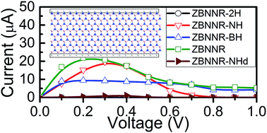
We investigate the charge transport properties of zigzag boron nitride nanoribbons (ZBNNRs) with various hydrogen passivations by employing density functional theory (DFT) combined with the non-equilibrium Green's function (NEGF) formalism. The calculated results reveal that the ZBNNR-based devices exhibit negative differential resistance (NDR) characteristics except those models whose both edges are passivated, due to the mechanism in which the overlap of bands near the Fermi level between the left and right electrodes gets smaller or disappears under a high bias. The NDR characteristics of the perfect ZBNNRs with one or two bare edges are weakly dependent on their widths. This is one intrinsic NDR characteristic of the ZBNNR-based devices, including some defective structures. The intuitive electronic current channels are plotted and analyzed to better understand the charge transport mechanisms. Our results suggest that the ZBNNR-based structures could be favorable candidates for preparing nanoscale NDR devices.
Hexagonal boron nitride (h-BN) single layer, the III–V analogue of graphene, has also attained much attention due to its super thermal and chemical stabilities.12–32 Two-dimensional (2D) h-BN sheet exhibits a direct energy gap of 4.78 eV,12 dramatically different from graphene which is a gapless semiconductor. Several groups have successively prepared the 2D boron nitride nanostructures.13–17 The purity is gradually improved and the cost is also decreasing.16,17 BN nanoribbons (BNNRs), mostly terminated with zigzag edges, has been successfully fabricated via boron nitride nanotube unwrapping since 2010.14,15 Some groups have theoretically investigated the electronic structures of the single layer BNNRs by considering different edge decorations,18 sample sizes,19 defects,20,21 doping,22 and external fields,23–26 etc. However, it needs to pay more attentions to the charge transport properties of BNNRs. Especially, it is one interesting topic to know how the edge decorations and ribbon widths affect their charge transport and applications in nanoscale electronics.
In this paper, we investigate the charge transport properties of zigzag BNNRs (ZBNNRs) by first-principles calculations within the local density approximation (LDA), and predict the intrinsic negative differential resistance characteristics in ZBNNRs with bare B edge, bare N edge, as well as bare B and N edges. The ZBNNRs with both edges passivated by hydrogen exhibit the wide gap semiconductor properties, and do not conduct electricity under finite bias voltages. However, the ZBNNRs with one or two bare edges show the metallic or half-metallic characteristics, and their current–voltage (I–V) curves all present the NDR behaviors rather than the linear characteristics. The current through the ZBNNRs with bare B edge belongs to the B → B hop current, which flows mainly along the bare B edge. However, for the ZBNNRs with bare N edge, there exist three current channels, i.e., N → B bond current, as well as B → N and N → N hop current channels under a low bias, but only N → B bond current channel under a high bias. All these current channels are along or close to the bare N edge. What's more, for the ZBNNRs with bare B and N edges, there exist four current channels under a low bias. There is one additional B → B hop current channel along the bare B edge, except that another three are same to the case of the ZBNNRs with bare N edge. While, only one N → B bond current channel is available under a high bias. Interestingly, the results also reveal that the NDR characteristic of the ZBNNRs is independent of ribbon widths, and survives in the defective ZBNNRs with certain boron or nitrogen atom vacancy defect. Unlike the graphene nanoribbons, which can present the NDR phenomena by defecting,9 doping,32 etc., it is the intrinsic characteristic for the ZBNNRs. Therefore, we propose that the ZBNNRs could be the favorable potential materials for NDR nanodevices.
The first-principles calculations of the charge transport properties of the ZBNNRs (with various hydrogen passivations at the edges) were performed by using the density functional theory (DFT) with the LDA combined with the non-equilibrium Green's function (NEGF) formalism as implemented in the ATK code.33–35 In the calculations, the geometry structure of each two-probe system was first relaxed until the absolute value of force acting on each atom is less than 0.05 eV Å−1 under the periodic boundary condition. The core electrons of all atoms were described by the Norm-conserving Troullier–Martins pseudopotentials,36 while the valence electrons were described by a double-ζ plus polarization (DZP) basis set. The Monkhorst–Pack k-points grid 1 × 1 × 100 was used to sample the Brillouin zone of the electrodes, and the real-space grid techniques were used with the energy cutoff of 100 Ry as a required cutoff energy in numerical integrations and the solution of Poisson equation using fast Fourier transform (FFT). We allow for an external bias Vb (Vb = VL − VR, and VL/R is the bias voltage applied on the left (L)/right (R) electrode) to be applied between the two electrodes. The applied bias thus shifts all energies in the left electrode, and a positive bias gives rise to an electric current from the left to the right electrode. The current I through these ZBNNR based devices can be calculated from the Landauer–Büttiker formula37
Here, we employ the band structure to understand the NDR behaviors of the 8-ZBNNR-based devices. Generally, the distinct charge transport properties should arise from the characteristics of band structures of the ZBNNRs with various hydrogen passivations, as shown in Fig. 2. The 8-ZBNNR-2H is the semiconductor with a gap of 3.85 eV, consistent with the previously published result.18 For the 8-ZBNNR-NH, it exhibits metallic feature, and there is one band crossing the Fermi level (EF), as shown in Fig. 2(b). The band is ascribed to the σ-dangling bond states at the edge B atoms (labeled as Bσ), which is mainly composed of a py orbital of edge B atoms according to the wave function at Γ point. For the case of 8-ZBNNR-BH, it exhibits half-metallic feature, as shown in Fig. 2(c). There are two bands crossing the EF level, which can be identified as the σ-dangling bond states at the edge N atoms (labeled as Nσ, composed of N py orbital) and the π states at the N atoms close to the bare N edge (labeled as Nπ, composed of N px orbital) according to the wave functions, respectively. Fig. 2(d) shows the band structure of the 8-ZBNNR which also presents metallic feature, consistent with the previous ab initio calculations.12 There are three bands crossing the EF level, which originates from the σ-dangling bond states at the edge N and B atoms, as well as the π states at the N atoms close to the bare N edge, respectively.
![]() | ||
Fig. 2 Band structure and wave functions of the (a) 8-ZBNNR-2H, (b) 8-ZBNNR-NH, (c) 8-BNNR-BH, and (d) 8-ZBNNR. The Fermi level is set at zero. |
For the semiconductor 8-ZBNNR-2H, the electrons are obviously forbidden to propagate through the nanojunction due to the wide band gap (shown in Fig. 2(a)), leading to zero current under the finite applied bias voltages, as shown in Fig. 1(b). Unlike the zigzag (ZGNRs) with odd-numbered chain which shows the linear trend,38 the I–V curve of 8-ZBNNR-NH exhibits an interesting NDR behavior. To understand this NDR phenomenon, we give the bias-dependent transmission spectra and band structures of both left and right electrodes for the 8-ZBNNR-NH in Fig. 3, which is the most intuitive representation of electronic structures and charge transport properties of a two-probe device. Under the positive bias, the energy bands shift downward and upward for the left and right electrodes, respectively. At the bias of 0.3 V, the Bσ band of left electrode has the largest overlapping region with that of the right electrode, between which the electron transmission from the Bσ band of the right electrode to that of the left electrode is allowable and the probability is close to 1. Fig. 3(b) and (c) show the electron transmission eigenstates and pathway at the EF under the bias of 0.3 V, respectively. It can be seen that the electron transmission channel is mainly distributed at the bare B edge (shown in Fig. 3(b)), and the local current (from the left to the right) belongs to the B → B hop current (shown in Fig. 3(c)). The energy overlapping region is larger than that of the bias window region at 0.3 V, but it gets smaller when the bias goes beyond 0.3 V and thus results in narrower transmission peak within the bias window. Therefore, a current peak appears at 0.3 V, and the NDR phenomenon is presented subsequently. For instance, when the bias increases up to 0.8 V, the Bσ band of left electrode has no overlaps with that of the right electrode. Thus, the electron transmission between them is forbidden, leading to zero transmission coefficients near the EF. Now then, the current decreases to zero at this threshold voltage (about 0.8 V).
Fig. 4(a) and (b) display the bias-dependent transmission spectra and band structures of both left and right electrodes for the 8-ZBNNR-BH. The band of the left electrode has large overlaps with that of the right electrode, especially in the negative energy region. Thus, the electron transmission between them is favorable. For instance, at the bias of 0.2 V, the transmission coefficient at −0.1 eV (chemical potential of the left electrode) is close to 2. Now, there are two transmission channels in the electron propagating through the nanoribbons, i.e., TE-N1 (contributed by the Nπ bands of the right and left electrodes), and TE-N2 (contributed by the Nσ bands of the two electrodes), respectively, as shown in the right side of Fig. 4(a). The transmission pathway (labeled as TP-N) indicates that the local currents mainly propagates along three channels, i.e., N → B bond current, as well as N → N and N → B hop current channels. When the bias goes beyond 0.2 V, the Nσ and Nπ bands of the left electrode shift away from the Fermi level, and they almost keep the same overlaps with that of the right electrode within the bias window. As a result, the transmission coefficient decreases slightly, and then the current through 8-ZBNNR-BH slightly declines (i.e., NDR behavior). While, when the bias reaches up to 0.8 V, only the Nπ band of the left electrode still overlaps with that of the right electrode within the bias window. Now, there is only one transmission channel, i.e., TE-N1′ (at −0.4 eV), which is contributed by the Nπ bands of the two electrodes. The local current mainly belongs to the N → B bond current according to the transmission pathway TP-N′. Therefore, unlike the case of 8-ZBNNR-NH, the current through 8-ZBNNR-BH at a high bias (greater than 0.8 V) only decreases to any non-zero steady value.
The NDR mechanisms of 8-ZBNNR-NH and 8-ZBNNR-BH also apply for the case of the 8-ZBNNR device. It is worth noting that, at the bias of 0.2 V (namely, at the current peak shown in Fig. 1(b)), there are three transmission channels at −0.06 eV, i.e., TE-BN1 (contributed by the Bσ bands of the two electrodes), TE-BN2 (contributed by the Nπ bands of the two electrodes), and TE-BN3 (contributed by the Nσ bands of the two electrodes), respectively. According to the corresponding transmission pathway at −0.06 eV, it is found that there are four local current channels, i.e., three N → N, N → B, and B → B hop current channels, as well as one N → B bond current channel. Nevertheless, each of the three bands (i.e., Bσ, Nσ, and Nπ) of the left electrode overlaps with that of the right electrode, as shown in Fig. 4(c). Within the bias window, the transmission coefficient is large and even close to 3 at −0.06 eV. Thus, the current peak appears at the bias of 0.2 V, which is larger than that of 8-ZBNNR-NH and 8-ZBNNR-BH devices. While, with the bias increasing, both Nσ and Nπ shift away from the EF level, even the overlaps of the Bσ and Nσ bands for both the left and right electrodes become smaller until they disappear successively. For instance, at the bias of 0.8 V shown in Fig. 4(d), only Nπ bands of the two electrodes overlap within the bias window. One transmission channel TE-BN1′ (at −0.4 eV, contributed by the Nπ bands of the two electrodes) is available, and the corresponding transmission pathway indicates the local current belongs to the N → B bond current. As a result, the transmission coefficients within the bias window decrease gradually, leading to the decreased current to any non-zero steady value at last, like the case of the 8-ZBNNR-BH, as shown in Fig. 1(b).
To further understand the effect of ribbon widths on the charge transport properties of ZBNNRs, the ribbon width is gradually increased. The I–V curves of four ZBNNRs-NH with a larger ribbon width (namely, 9-ZBNNR-NH, 10-ZBNNR-NH, 11-ZBNNR-NH, and 12-ZBNNR-NH) were further explored and plotted in Fig. 5(a), from which we can see that these four ZBNNRs-NH with a larger width present the same charge transport properties compared to the case of the 8-ZBNNR-NH. This is mainly ascribed to that they have the very similar band structures around the EF level and thus the same NDR mechanism simultaneously. The same charge transport properties were also found for the cases of ZBNNR-BH and ZBNNR with a larger ribbon width. Unlike the ZGNRs, the ZGNRs with odd-numbered chains present entirely different charge transport properties from that with even-numbered chains in spite of their similar band structures.38 It reveals that under the finite biases the charge transport properties of perfect ZBNNRs with one or two bare edges do not show obvious dependencies on their widths. The NDR is one intrinsic characteristic of the perfect zigzag boron nitride nanoribbons, which is different from that it can be obtained in graphene nanoribbons by defecting,9 doping,32 etc.
In addition, defects (such as vacancies) are generally unavoidable during the growth process of a sample.13 Whether a vacancy defect affects the intrinsic NDR characteristics of ZBNNRs is unknown. Here, two models are considered, i.e., 8-ZBNNR-NH with a boron atom vacancy defect (labeled as 8-ZBNNR-NHBd) and with a nitrogen atom vacancy defect (labeled as 8-ZBNNR-NHNd) in the central scattering region, as shown in the insets of Fig. 5(b) and (c). Their I–V curves are depicted in Fig. 5(b) and (c). We can see that the NDR behaviors still survive in the two defective structures. The only difference is that their current amplitudes decrease by several orders of magnitude. This is due to the fact that the vacancy defect breaks the edge states and produces some localized defect-induced states, which suppress the electron transmission and diminish the current. Therefore, some ZBNNR-based nanoscale NDR devices owning different current peaks and peak to valley ratios with various orders of magnitude are promising candidates in devices, such as digital applications,39,40 amplification,41 and oscillators,42 etc. What's more, the BCN nanoribbons also depict the NDR behaviors,22 which demonstrates that the intrinsic NDR characteristics of ZBNNRs are preserved in spite of the carbon-doping.
This journal is © The Royal Society of Chemistry 2014 |