
Performance improvement in Cd-free Cu(In,Ga)Se2 solar cells by modifying the electronic structure of the ZnMgO buffer layer
Chang-Soo Lee,
Suncheul Kim,
Young-Min Shin,
Byung Guk Park,
Byung Tae Ahn* and
HyukSang Kwon*
Department of Materials Science and Engineering, Korea Advanced Institute of Science and Technology, 291 Daehak-ro, Yuseong-gu, Daejeon 305-701, Republic of Korea. E-mail: btahn@kaist.ac.kr; hskwon@kaist.ac.kr
First published on 7th August 2014
Abstract
ZnMgO thin film is a potential buffer layer in Cu(In,Ga)Se2 (CIGS) solar cells. ZnMgO film can be uniformly deposited, and the composition of Mg can be precisely controlled by the atomic layer deposition process. The conduction band offset at the ZnMgO/CIGS interface can be reduced by increasing the Mg content in the ZnMgO buffer. The ZnMgO buffer layer with 20% Mg content has shown the best cell efficiency in the AZO/i-ZnO/ZnMgO/CIGS structure. In this study, with the removal of i-ZnO from the structure, the cell efficiency was improved from 13.9 to 15.2% due to a decrease in the series resistance and an increase in the shunt resistance. Then, the 40 nm thick Zn0.8Mg0.2O buffer layer was modified to a Zn0.9Mg0.1O (20 nm)/Zn0.8Mg0.2O (20 nm) bilayer, in which the thickness of the Zn0.8Mg0.2O layer was reduced while the total thickness was maintained to minimize plasma damage from the subsequent AZO deposition by sputtering. With the bilayer buffer, the efficiency of the CIGS solar cell was further increased from 15.2 to 16.4%. In particular, the open circuit voltage and fill factor were significantly improved. Fewer deep level states in the Zn0.9Mg0.1O/Zn0.8Mg0.2O bilayer compared to a single Zn0.8Mg0.2O layer may be responsible for the improved performance.
Introduction
Cu(In,Ga)Se2 (CIGS)-based solar cells have reached a laboratory efficiency of more than 20%, where a cadmium sulfide (CdS) buffer layer acts as an important counterpart to the CIGS absorber.1,2 However, for the commercialization of sustainable energy systems, the CdS buffer, which contains the environmentally hazardous Cd, needs to be excluded from the structure of CIGS solar cells. Over the past decade, ZnMgO films have attracted increasing interest in the field of photovoltaics because of their potential application as an alternative Cd-free buffer material for CIGS solar cells.3,4 The advantage of ZnMgO film is that it allows adjustment of the band gap with various levels of Mg content. Indeed, the band gap can be increased from 3.2 to 3.9 eV by increasing the Mg content.5,6 With a wider band gap, more incident light in the short wavelength region can be absorbed in the CIGS absorber than in the CdS film. In addition, by using the tunable band gap, the conduction band offset between the buffer layer and the absorber material can be adjusted appropriately to maximize the electron injection from the absorber layer to the buffer layer.7,8To date, radio-frequency (RF) magnetron sputtering and atomic layer deposition (ALD) have commonly been used to deposit ZnMgO film. An efficiency of 16.2% was achieved by Matsushita Electric Industrial Corporation for a laboratory-scale CIGS solar cell with a sputtered ZnMgO buffer layer.3 However, in the sputtering process, highly energetic particles in the plasma can seriously damage the surface of the CIGS absorber, which affects the quality of the buffer/absorber interface, and in turn, the device performance.9 To avoid this problem, an ALD process for ZnMgO deposition was introduced. ALD has several advantages over other deposition methods such as good film quality, accurate thickness control, excellent conformality, and uniformity over large areas, since ALD is characterized by the alternate exposure of chemical species with self-limiting surface reactions. Hultqvist et al. reported an efficiency of 18.1% for a CIGS solar cell with an ALD ZnMgO buffer layer, representing the highest value for CIGS devices with a ZnMgO buffer layer.10,11
In our previous studies, ZnMgO thin films with a wurzite structure were deposited by ALD using diethylzinc (DEZ) and bis-ethyl-cyclopentadienyl-magnesium (Mg(EtCp)2) as metal precursors and water vapor as a reactant.12 The Mg content in the ZnMgO film was closely matched to the ALD cycle ratio of ZnO and MgO, which indicated that the composition of the films could be precisely controlled by adjusting the ALD cycle ratio of each monolayer. We confirmed that the bandgap energy of the ZnMgO films increased from 3.25 to 3.76 eV as the Mg content increased from x = 0 to x = 0.25. Additionally, we also investigated the electronic band structure at the ZnMgO/Cu(In,Ga)Se2 interface to determine the optimum composition of the ZnMgO films using the depth profile techniques of X-ray photoelectron spectroscopy and ultraviolet photoelectron spectroscopy.7 The study revealed that a flat conduction band offset could be obtained at the ZnMgO/Cu(In0.7Ga0.3)Se2 interface when the composition of ZnMgO was Zn0.8Mg0.2O. The valence band offset was 2.55 eV after consideration of the small band bending in the interface region. Those experimental results suggest that the appropriate amount of Mg in the ZnMgO film is 20% for the optimum conduction band offset at the ZnMgO/Cu(In,Ga)Se2 interface. Minemoto et al. also reported that sputtered Zn0.83Mg0.17O with a band-gap energy of 3.6 eV made a small spike at the ZnMgO/CIGS interface.8 Based on an understanding of the electronic structure, we fabricated CIGS solar cells with a ZnMgO buffer and analyzed their photovoltaic properties. We then designed the electronic structure of the buffer layer to enhance the cell performance.
Experimental
ZnMgO films were grown on CIGS absorbers at 120 °C using a vertical hot-wall type ALD reactor. For ZnMgO film growth, DEZ and Mg(EtCP)2 were used as metal precursors and water vapor was used as a reactant. High-purity Ar gas was used as a purging and carrier gas. We used a growth sequence for the ZnO monolayer of DEZ exposure of 0.1 s, Ar purging of 1.5 s, H2O exposure of 0.1 s, and Ar purging of 3 s. The MgO monolayer was prepared by Mg(EtCP)2 exposure of 2 s, Ar purging of 2 s, H2O exposure of 0.1 s, and Ar purging of 3 s. For the Zn0.8Mg0.2O and Zn0.9Mg0.1O films, a cycle of the MgO ALD sequence was introduced once every 4 and 9 cycles of the ZnO ALD sequence.13CIGS solar cells with a ZnMgO buffer layer with various amounts of Mg content were fabricated. The CIGS light absorber was deposited on Mo-coated soda lime glass (SLG) by a three-stage co-evaporation process: In, Ga, and Se evaporation at 350 °C in the first stage; Cu and Se evaporation at 550 °C in the second stage; and In, Ga, and Se evaporation at 550 °C in the third stage.14 The thickness of the CIGS absorber layer was 2 μm. A ZnMgO film was then deposited on the CIGS absorber layer using an ALD process, and intrinsic ZnO (i-ZnO) and Al-doped ZnO (AZO) window layers were deposited by RF magnetron sputtering.9 An Al metal grid was formed by Al evaporation on the window layer. The complete structure of the solar cell was made with an AZO/i-ZnO/ZnMgO/CIGS/Mo/SLG substrate. The devices were then annealed at 200 °C for 2 min by a rapid thermal annealing process.
The morphology of the ZnMgO film and the interface morphology between the ZnMgO and CIGS were examined by scanning electron microscopy (SEM) and transmission electron microscopy (TEM). The resistivity of the buffer layers was measured using a 4-point probe. The photovoltaic parameters were measured at 100 mW cm−2 intensity with AM1.5 spectra after the cells were illuminated for 15 min under one-sun condition using a solar simulator. The reverse saturation current of the CIGS solar cells was measured using a probe station in a dark cabinet. A low-temperature photoluminescence (LTPL) analysis at 10 K was carried out by excitation of a He–Cd laser with 325 nm wavelength to find deep level defects in the ZnMgO film.
Results and discussion
Fig. 1(a) and (b) show the SEM images of the Zn0.8Mg0.2O films deposited on the glass substrate and the CIGS absorber. The film deposited on the glass substrate (Fig. 1a) clearly shows a uniform deposition with thickness of around 40 nm. The film deposited on CIGS film (Fig. 1b) also shows a uniform thickness and good step coverage. | ||
| Fig. 1 SEM images of ZnMgO films deposited on a glass substrate (a) and the CIGS absorber (b). | ||
Fig. 2 shows a TEM image of the Zn0.8Mg0.2O/CIGS interface. The Zn0.8Mg0.2O layer shows an image contrast due to defects such as dislocations and stacking faults. Since the lattice constant of ZnMgO is much smaller than that of CdS, it was expected that many interface defects will exist at the interface.
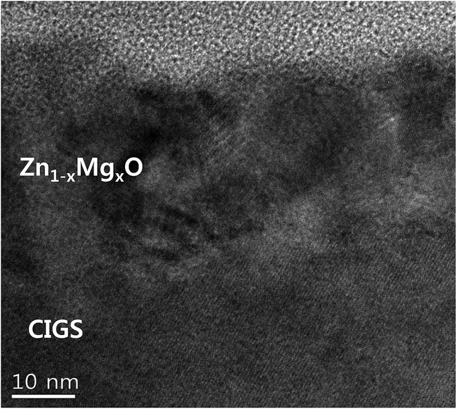 | ||
| Fig. 2 TEM image of the ZnMgO/CIGS interface. | ||
Fig. 3 shows the J–V curves of the Zn0.8Mg0.2O/Cu(In0.7Ga0.3)Se2 solar cells with various buffer thicknesses. The Mg content in the ZnMgO buffer was fixed at 20% because of a conduction band offset of nearly zero.7 As the thickness increased from 40 to 80 nm the conversion efficiency, η, decreased from 12.4 to 7.0%. The shunt resistances, Rshs, of the cells with 40, 60, and 80 nm thickness were 420, 280, and 140 Ω cm2, respectively, and the series resistances, Rss, of the cells with 40, 60, and 80 nm thickness were 1.8, 2.4, and 10.7 Ω cm2, respectively. With the increase of buffer thickness from 40 to 60 nm, the open circuit voltage, Voc, was drastically dropped (0.54 to 0.45 V), while the short circuit current, Jsc, did not change. With a further increase of the buffer thickness from 60 to 80 nm, the Jsc drastically dropped (35 to 27 mA cm−2), while the Voc values were similar. The significant drop of Jsc with the 80 nm thick buffer layer was due to the high resistivity of the buffer layer with an Rs value of 10.7 Ω cm2. There might also have been some optical scattering loss through the thicker buffer. It is clear that the thickness of ZnMgO buffer should be as thin as possible to minimize the resistance contribution of the buffer layer. The origin of the lower Voc in the cells with 60 and 80 nm thick buffers compared to the cell with a 40 nm thick buffer was due to the Zn diffusion into CIGS during the ALD process.15 Excess Zn incorporation in the CIGS film enhanced the recombination rate and lowered the Voc. Since the cell performance was best with a 40 nm thick buffer layer, that thickness was selected for further experiment.
 | ||
| Fig. 3 Illuminated J–V curves of Zn0.8Mg0.2O/Cu(In0.7Ga0.3)Se2 solar cells with various buffer thicknesses. | ||
Fig. 4 shows the J–V curves of the ZnMgO/Cu(In0.7Ga0.3)Se2 solar cells with various Mg contents in the ZnMgO buffer. The thickness of the ZnMgO was 40 nm and the Ga content in the CIGS absorber was 0.3 on average. The photovoltaic parameters, such as Voc, Jsc, and fill factor (FF), are summarized in Table 1. As the Mg content in the Zn1−xMgxO buffer increased from x = 0.1 to 0.2, the cell conversion efficiency increased from 7.5to 13.6%. Then, the cell efficiency decreased with further increase of the Mg content in the ZnMgO buffer. It has been reported that the conduction band offset (CBO) at the ZnMgO/CIGS interface plays an important role in charge collection.7 The CBO is minimum when the Mg content is x = 0.2 and the efficiency was best as suggested. In Table 1, the efficiency was mostly dependent on the change of the open circuit voltage, Voc, and fill factor, FF.
 | ||
| Fig. 4 Illuminated J–V curves of ZnMgO/Cu(In0.7Ga0.3)Se2 solar cells with various Mg contents. | ||
| Buffer | Voc (V) | Jsc (mA cm−2) | FF | η (%) | Jo (A cm−2) | A | Rsh (Ω cm2) | Rs (Ω cm2) |
|---|---|---|---|---|---|---|---|---|
| CdS | 0.610 | 32.4 | 0.73 | 14.4 | 1.9 × 10⁻⁸ | 1.43 | 1720 | 0.61 |
| Zn0.9Mg0.1O | 0.424 | 34.1 | 0.52 | 7.5 | 4.9 × 10⁻⁴ | 2.21 | 100 | 0.76 |
| Zn0.83Mg0.17O | 0.506 | 33.9 | 0.53 | 9.2 | 3.2 × 10⁻⁵ | 2.15 | 230 | 0.84 |
| Zn0.8Mg0.2O | 0.565 | 34.9 | 0.67 | 13.6 | 6.8 × 10⁻⁷ | 1.89 | 1020 | 0.63 |
| Zn0.75Mg0.25O | 0.541 | 34.7 | 0.66 | 12.3 | 1.7 × 10⁻⁶ | 1.95 | 580 | 0.62 |
Fig. 5 shows the dark J–V curves of the ZnMgO/CIGS solar cells with various Mg contents. The diode parameters such as reverse saturation current, Jo, diode ideality factor, A, shunt resistance, Rsh, and series resistance, Rs, of ZnMgO/CIGS cells with various Mg contents are also summarized in Table 1. The Jo decreased as the Mg content increased from 0.1 to 0.2 and then increased with a further increase of the Mg content. The diode ideality factor decreased from 2.21 to 1.89 as the Mg content increased. In Table 1, the efficiency was mostly dependent on the changes of Voc and FF. A high Voc and large FF were obtained when Jo was small and Rsh was large. Since the relation between Voc and Jo is expressed as Voc = AkT/q![[thin space (1/6-em)]](https://www.rsc.org/images/entities/char_2009.gif) ln(Jsc/Jo + 1), Voc increases as Jo decreases. Note that Jo, which represents the recombination current through the space-charge region, is an important parameter and should be as low as possible.
ln(Jsc/Jo + 1), Voc increases as Jo decreases. Note that Jo, which represents the recombination current through the space-charge region, is an important parameter and should be as low as possible.
 | ||
| Fig. 5 Dark J–V curves of ZnMgO/Cu(In0.7Ga0.3)Se2 solar cells with various Mg contents. | ||
As the Mg content in ZnMgO layer increases (in case of less than 20%), the magnitude of conduction band cliff at the buffer/CIGS interface becomes small and the Rsh increases.7 However, the Rsh decreased with further Mg content. The Rsh reduction was explained in Fig. 7 paragraph from the point of the increase of deep-level defect in ZnMgO buffer.
The surface recombination could occur by two different mechanisms: (1) by a tunneling recombination in which the electrons in TCO layer and the free holes in the CIGS film recombine through the trap centers at the ZnMgO/CIGS interface and (2) by surface recombination in which the free electrons and free holes in the CIGS film recombine through the trap centers at the ZnMgO/CIGS interface. In either case, the generation of trap centers could affect Jo. The latter surface recombination is analogous to bulk recombination. While bulk recombination occurs by the recombination of free electrons and holes through trap centers that exist in the bulk, surface recombination occurs by the free electrons and holes at the surface trap centers. The equilibrium electron concentration at the surface is several order higher than that in the bulk due to surface depletion and also deep-level defect concentration is also higher than that in the bulk. If a conduction band notch exists at the buffer/CIGS, the light-generated free carriers could accumulate at the interface and the recombination will be much more enhanced.
The efficiency value with Mg = 0.2 was still low compared to the results reported by other research groups.10–12 In a comparison of our results with those from leading research groups, we found that one of the main reasons for the difference in the cell efficiency is the relatively low fill factor. One of the factors that affects the fill factor is the series resistance. For this purpose, we removed the i-ZnO layer from the AZO/i-ZnO/Zn0.8Mg0.2O/CIGS structure.
Fig. 6 shows the J–V curves (a) and R–J curves (b) of the Zn0.8Mg0.2O/CIGS solar cells with and without the i-ZnO layer. For AZO/i-ZnO deposition on the cells, a 40 nm thick i-ZnO was deposited at a 50 W sputtering power and a 150 nm thick AZO was deposited at a 260 W sputtering power. For AZO deposition without i-ZnO deposition, a 190 nm thick AZO film was deposited at a 200 W sputtering power to reduce sputtering damage to the ZnMgO buffer layer. The photovoltaic parameters obtained from Fig. 6a and b and the diode parameters are summarized in Table 2. The removal of i-ZnO increases the cell efficiency from 13.9 to 15.2%, which is a big enhancement. Note that the FF was notably increased (9.1% increase) by the removal of the i-ZnO layer in the cell, while Voc and Jsc were little changed. The Rsh greatly increased and Rs decreased significantly.
 | ||
| Fig. 6 Illuminated J–V curves (a) and R–J curves (b) of ZnMgO/CIGS solar cells with and without an intrinsic ZnO layer. | ||
| Voc (V) | Jsc (mA cm−2) | FF | η (%) | Jo (A cm−2) | A | Rsh (Ω cm2) | Rs (Ω cm2) | |
|---|---|---|---|---|---|---|---|---|
| With i-ZnO | 0.600 | 35.0 | 0.66 | 13.9 | 2.5 × 10⁻⁷ | 2.03 | 720 | 0.53 |
| W/o i-ZnO | 0.596 | 35.5 | 0.72 | 15.2 | 2.7 × 10⁻⁷ | 1.59 | 1130 | 0.20 |
| % change | −0.7% | 1.4% | 9.1% |
As a reference, we fabricated CdS/CIGS solar with and without i-ZnO. The efficiencies of the CdS/CIGS solar cells with and without i-ZnO were 14.4 (Jsc = 32.4 mA cm−2, Voc = 0.61, FF = 0.73) and 7.3% (Jsc = 20.4 mA cm−2, Voc = 0.57, FF = 0.63), respectively. The Rsh and Rs of the cells with i-ZnO were 1720 and 0.61 Ω cm2, respectively, while those of the cells without i-ZnO were 330 and 1.50 Ω cm2, respectively. It was clear that the Jsc and Rsh dropped significantly without the i-ZnO layer. This indicates that i-ZnO acts as a protection from sputtering damage and a tunneling suppression layer.
With the removal of i-ZnO in the ZnMgO/CIGS structure several notable results were seen. First, the Rsh increased from 720 to 1130 Ω cm2. Second, the Rs was reduced from 0.53 to 0.20 Ω cm2. As a result, the FF was greatly improved from 0.66 to 0.72 (9.1% increase). Third, the Jsc and Voc were not significantly changed, unlike the CdS/CIGS structure in which those values significantly dropped as mentioned in the previous paragraph. In the CdS/CIGS structure, i-ZnO acted as a buffer layer that suppressed the tunneling recombination between the free electrons in the AZO electrode and the free holes in the CIGS films; thus we conclude that the existence of i-ZnO is necessary in CdS/CIGS solar cells. In the ZnMgO/CIGS structure, it is seen that ZnMgO buffer itself covered the role of the i-ZnO layer so that the i-ZnO layer was unnecessary.
Fig. 7 shows the LTPL spectra of the ZnMgO thin films with various Mg contents. In the i-ZnO film, two emission peaks are observed: an ultraviolet (UV) peak located at approximately 3.2 eV and a green peak located at approximately 2.4 eV. The UV emission peak was due to band-to-band recombination, and the green emission peak was due to deep-level defect recombination.16 The deep-level defect in ZnO is known as an oxygen vacancy.16 As the Mg content in ZnMgO film increased, the UV emission peak shifted to higher photon energy and the intensity of the green peak became dominant to that of the UV peak. The shift of the UV emission peak with Mg incorporation was due to the increase of the band gap.17,18 The strong green emission suggests that more deep-level defects were generated in the ZnMgO films with Mg incorporation, which indicates that less oxygen was supplied during the MgO ALD cycle. From the LTPL spectra, the ZnMgO film deposited by the ALD process contains more deep-level defects with an increase in the Mg content.
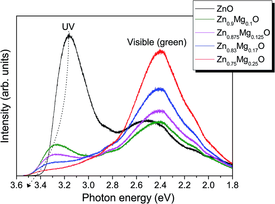 | ||
| Fig. 7 LTPL spectra of the ZnMgO thin films with various Mg contents. | ||
Thus far, the CIGS solar cell with a 40 nm thick Zn0.8Mg0.2O buffer layer had the best cell performance in our experiment as seen in Fig. 4. It is seen that the tunneling recombination through the buffer layer played a key role in Fig. 5 and 6. Since the deep-level defects increased as the Mg content increased in the ZnMgO film, it is necessary to reduce the Mg content in the buffer layer so that the tunneling recombination through the ZnMgO buffer layer can be lowered.
For this purpose, we introduced a bilayer buffer in the form of a Zn0.9Mg0.1O/Zn0.8Mg0.2O film instead of a single Zn0.8Mg0.2O film; the total thickness is thus maintained at 40 nm, but the thicknesses of Zn0.9Mg0.1O and Zn0.8Mg0.2O are 20 nm each. Since the intensity of green peak emission is low and similar to that of i-ZnO, it is expected that the concentration of deep-level defects in Zn0.9Mg0.1O is much smaller compared to Zn0.8Mg0.2O.
Fig. 8 illustrates the schematic band structures of the CIGS solar cells with a single layer buffer (a) and a bilayer buffer (b). Tunneling recombination could occur through the deep-level trap states in the Zn0.8Mg0.2O layer. With the addition of Zn0.9Mg0.1O which has fewer deep-level defects and a comparable band gap with Zn0.8Mg0.2O the tunneling of electrons from the AZO electrode might be suppressed. As a result it is expected that the tunneling through the ZnMgO buffer is further lowered by employing the bilayer structure.
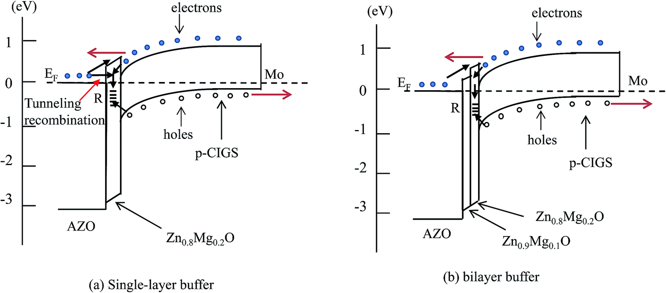 | ||
| Fig. 8 Schematic diagram of the electronic band structure for CIGS solar cells with a single-layer buffer (a) and a bilayer buffer (b). | ||
Fig. 9 shows the illuminated J–V curves (a) and the dark J–V curves (b) of the ZnMgO/CIGS solar cells with a Zn0.8Mg0.2O single-layer buffer and a Zn0.9Mg0.1O/Zn0.8Mg0.2O bilayer buffer. The conversion efficiency of the CIGS solar cell with the Zn0.8Mg0.2O buffer layer is 15.2%, while that of the CIGS solar cell with a bilayer buffer is 16.4% (1.2% efficiency increase). The device with the bilayer buffer had a notable increase of Voc (4.7% increase) and a significant increase of FF (2.8% increase) compared to those factors for the device with the single Zn0.8Mg0.2O layer.
 | ||
| Fig. 9 Illuminated J–V curves (a) and dark J–V curves (b) of ZnMgO/CIGS solar cells with a Zn0.8Mg0.2O single-layer buffer and Zn0.9Mg0.1O/Zn0.8Mg0.2O bilayer buffer. | ||
The open circuit voltage was closely related to the reverse saturation current of the diode device. The reverse saturation currents, Jo, of the cells with the single layer and bilayer were 2.7 × 10⁻⁷ and 4.3 × 10⁻⁸ A cm−2, respectively, as shown in Table 3. Note that the reverse saturation current of the cell with the bilayer buffer was much smaller than that of the cell with the single layer buffer, although the width of the Zn0.8Mg0.2O potential was thinner in the bilayer buffer. Also note that the Rsh was increased from 1130 to 1230 Ω cm2 with the bilayer buffer. The lower Jo and larger Rsh in the cell with the bilayer buffer might be attributed to the presence of fewer deep-level defects, which can act as recombination centers.
| Buffer layer | Voc (V) | Jsc (mA cm−2) | FF | η (%) | Jo (A cm−2) | A | Rsh (Ω cm2) | Rs (Ω cm2) |
|---|---|---|---|---|---|---|---|---|
| Zn0.8Mg0.2O | 0.596 | 35.5 | 0.72 | 15.2 | 2.7 × 10⁻⁷ | 1.59 | 1130 | 0.20 |
| Zn0.9Mg0.1O/Zn0.8Mg0.2O | 0.624 | 35.4 | 0.74 | 16.4 | 4.3 × 10⁻⁸ | 1.37 | 1230 | 0.17 |
| % change | 4.7% | — | 2.8% |
In the cell with the single-layer Zn0.8Mg0.2O buffer, the electrons from the ZnO electrode can be easily captured in deep-level defects in the buffer and can then recombine with holes in the CIGS absorber, as shown in Fig. 8a. On the other hand, in the cell with the bilayer Zn0.9Mg0.1O/Zn0.8Mg0.2O buffer, the electron injection from the ZnO electrode can be blocked by the substantially less defective Zn0.9Mg0.1O buffer, shown in Fig. 8b. Therefore, the Jo value of the cell with the Zn0.9Mg0.1O/Zn0.8Mg0.2O bilayer buffer was smaller than that of the cell with the Zn0.8Mg0.2O single-layer buffer, resulting in a higher open circuit voltage.
Conclusion
ZnMgO buffer layers with various Mg contents were deposited using an ALD process for Cd-free buffer Cu(In,Ga)Se2 solar cells. We found that the optimum composition of the ZnMgO buffer was Zn0.8Mg0.2O and the efficiency was low due to low Voc and FF, which mainly originate from the junction parameters, including Jo and Rsh. To reduce the Rs of the ZnMgO/CIGS solar cell, the 50 nm thick i-ZnO window layer that was used for the conventional CdS/CIGS solar cell was removed. As result, the Rsh increased from 720 to 1130 Ω cm2 and the Rs value decreased from 0.53 to 0.20 Ω cm2, causing an increase of the FF from 0.66 to 0.72 and cell efficiency from 13.9 to 15.2%. Then, the 40 nm thick Zn0.8Mg0.2O buffer layer was modified into a Zn0.9Mg0.1O(20 nm)/Zn0.8Mg0.2O(20 nm) bilayer buffer in which a Zn0.9Mg0.1O layer with fewer deep-level defects was introduced. As a result, the cell conversion efficiency was improved from 15.2 to 16.4%. The increase of Voc and FF were the main contributors to the cell efficiency improvement. In this case, the Jo value decreased by one order of magnitude (from 2.7 × 10⁻⁷ to 4.3 × 10⁻⁸ A cm−2) and the Voc increased. The decrease of Jo and the subsequent increase of Voc were attributed to the suppression of tunneling recombination by blocking electron transport from the AZO electrode to the ZnMgO buffer with the Zn0.9Mg0.1O composition with fewer deep-level defects.Acknowledgements
This work was supported by the Engineering Research Center Program (2012-0001167), the Priority Research Center Programs (2011-0031407), and the KAIST EEWS Program (EEWS-2012-N01120013), funded by the Korean Ministry of Education and Technology (MEST).References
- I. Repins, M. A. Contreras, B. Egaas, C. DeHart, J. Scharf, C. L. Perkins, B. To and R. Noufi, Progr. Photovolt.: Res. Appl., 2008, 16, 235 CrossRef CAS PubMed.
- P. Jackson, D. Hariskos, E. Lotter, S. Paetel, R. Wuerz, R. Menner, W. Wischmann and M. Powalla, Progr. Photovolt.: Res. Appl., 2011, 19, 894 CrossRef CAS PubMed.
- N. Takayuki, A. Taikan, S. Takuya, S. Shin-ichi, H. Shigeo and H. Yasuhiro, Proceedings of the 29th IEEE Photovoltaic Specialists Conference, New Orleans, 2002 Search PubMed.
- T. Törndahl, C. Platzer-Björkman, J. Kessler and M. Edoff, Progr. Photovolt.: Res. Appl., 2007, 15, 225 CrossRef PubMed.
- T. Gruber, C. Kirchner, R. Kling, F. Reuss and A. Waag, Appl. Phys. Lett., 2004, 84, 5359 CrossRef CAS PubMed.
- A. Ohtomo, M. Kawasaki, T. Koida, K. Masubuchi, H. Koinuma, Y. Sakurai, Y. Yoshida, T. Yasuda and Y. Segawa, Appl. Phys. Lett., 1998, 72, 2466 CrossRef CAS PubMed.
- C. S. Lee, L. Larina, Y.-M. Shin, E. A. Al-Ammar and B. T. Ahn, Phys. Chem. Chem. Phys., 2012, 14, 4789 RSC.
- T. Minemoto, Y. Hashimoto, T. Satoh, T. Negami, H. Takakura and Y. Hamakawa, J. Appl. Phys., 2001, 89, 8327 CrossRef CAS PubMed.
- D. H. Shin, J. H. Kim, Y. M. Shin, K. H. Yoon, E. A. Al-Ammar and B. T. Ahn, Progr. Photovolt.: Res. Appl., 2013, 21, 217 CrossRef CAS PubMed.
- A. Hultqvist, C. Platzer-Björkman, T. Törndahl, M. Ruth and M. Edoff, Proceedings of the 22nd European Photovoltaic Solar Energy Conference, Milan, 2007 Search PubMed.
- W. Witte, S. Spiering and D. Hariskos, Vak. Forsch. Prax., 2014, 26(1), 23 CrossRef CAS PubMed.
- C. S. Lee, Y. M. Shin and B. T. Ahn, ECS Trans., 2011, 41, 213 CAS.
- C. Platzer-Björkman, T. Törndahl, A. Hultqvist, J. Kessler and M. Edoff, Thin Solid Films, 2007, 515, 6024 CrossRef PubMed.
- K. H. Kim, K. H. Yoon, J. H. Yun and B. T. Ahn, Electrochem. Solid-State Lett., 2006, 9, A382 CrossRef CAS PubMed.
- C. S. Lee, S. C. Kim, E. A. Al-Ammar, H. S. Kwon and B. T. Ahn, ECS J. Solid State Sci. Technol., 2014, 3(6), Q99 CAS.
- D. H. Park, Y. H. Cho, D. H. Shin and B. T. Ahn, Current Photovoltaic Research, 2013, 1, 115 Search PubMed.
- H. Shibata, H. Tampo, K. Matsubara, A. Yamada, K. Sakurai, S. Ishizuka, S. Niki and M. Sakai, Appl. Phys. Lett., 2007, 90, 124104 CrossRef PubMed.
- C. J. Pan, H. C. Hsu, H. M. Cheng, C. Y. Wu and W. F. Hsieh, J. Solid State Chem., 2007, 180, 1188 CrossRef CAS PubMed.
| This journal is © The Royal Society of Chemistry 2014 |