
Tuning the electron transport properties of boron-nitride nanoribbons with electron and hole doping
L. L. Songab,
X. H. Zheng*a,
H. Haoa,
J. Lana,
X. L. Wanga and
Z. Zengac
aKey Laboratory of Materials Physics, Institute of Solid State Physics, Chinese Academy of Sciences, Hefei 230031, China. E-mail: xhzheng@theory.issp.ac.cn; Fax: +86-551-65591434; Tel: +86-551-65591150
bSchool of Electronic Science and Applied Physics, Hefei University of Technology, Hefei 230009, China
cDepartment of Physics, University of Science and Technology of China, Hefei 230026, China
First published on 17th September 2014
Abstract
By first principles calculations based on the density functional theory and nonequilibrium Green’s function technique, we have studied the electronic and transport properties of C-doped zigzag-edged boron-nitride nanoribbons (ZBNNRs). Due to the two sub-lattices in boron-nitride nanoribbons (BNNRs), C substitutions at B sites and N sites naturally provide ways for electron doping and hole doping. Different combinations of the C chain substitution schemes are utilized to tune the electron transport of nano junctions constructed with ZBNNRs. It is found that, either substitution for B or N by C, in symmetric doping, the junction always behaves as a good conductor. However, in the asymmetric doping, the performance of the junctions highly depends on the positions of the C chain. When the C atoms are doped at opposite edges on the two sides of the junction, there is no current across the junction although dopings at B site and N site can both transform a BNNR from an insulator into a metal. Interestingly, when the doping sites are moved to the middle of the ribbons, the junctions conduct very well and negative differential resistance (NDR) is observed due to the special alignment of the energy bands of the two leads.
1 Introduction
Graphene and its nanostructures are among the most promising building blocks for future nanoelectronic devices and have attracted ever-increasing attention due to their novel structure and enriched electronic and magnetic properties.1–3 Extensive studies on graphene have also stimulated great interest in its isomorph—single layers of hexagonal boron-nitride (h-BN), which replaces carbon atoms in graphene with alternating boron and nitrogen atoms in the sp2 lattice structure. Although a h-BN layer has a similar structure to that of graphene, it possesses a number of properties different from its carbon counterpart. A pure h-BN layer is a semiconductor with a wide band gap, high chemical inertness, thermal stability, enhanced oxidation resistance and good optical properties.4–6 These distinctions make h-BN uniquely attractive for applications in electronics, photonics and nanocomposites.7,8Similar to graphene, h-BN layers can be terminated in one of the dimensions to obtain quasi-one-dimensional materials, known as BN nanoribbons (BNNRs). Depending on the direction of termination, there are two types of BNNRs, based on their edge shapes, called zigzag-edged BNNRs and armchair-edged BNNRs, respectively. Armchair-edged BNNRs are usually nonmagnetic semiconductors. The corresponding energy gap is found to oscillate with increasing ribbon width. However, the gap of zigzag-edged BNNRs (ZBNNRs) decreases monotonically as the ribbon width increases.9–11 Moreover, depending on their edge passivation, ZBNNRs could be either magnetic or nonmagnetic.12–17 As proved by previous studies on ZBNNRs, the electronic and magnetic properties in these ribbons are easily modified by different methods, such as by external electric field,9 defects,18,19 hydrogenation,20 impurity or molecular doping.21,22 Especially, it has been demonstrated that C-doping is an efficient approach to tune the optical, chemical, electronic, and magnetic properties of BN nanomaterial and extend their application.23–27 Recently, Park et al. have shown that C-doped h-BN has extraordinary properties with possible application in optics, magneto-optics and opto-electronics.28 After C doping, the hydrogen storage capacity of h-BN with transition-metal dispersion is obviously uplifted.29 This makes h-BN an exceptional candidate in high capacity hydrogen storage. Moreover, Beheshtian et al. found that doping BNNRs with a zigzag line of carbon atoms decreases the ribbon’s band gap, and the electric polarization of the doped BNNRs depends on the types of atoms (B or N) that surround the dopants.30 Even in the absence of an external electric field, carbon chain-doped zigzag BNNRs with one H-saturated boron edge and one bare carbon edge exhibit half-semiconducting → half-metallic → metallic electronic transition behaviors as the number of zigzag carbon chains replacing the zigzag boron–nitrogen chains gradually increases.31
Due to enriched properties and widespread application of C-doped h-BN, both experimental and theoretical researchers are motivated to propose various ways for its fabrication. Recently, electron-beam induced substitution has been successfully applied for doping C atoms in h-BN and BN nanotubes.32,33 More interestingly, Liu et al. proposed a novel approach of constructing custom-designed C doped h-BN via CO molecules interacting with the vacancy defect in h-BN using the density functional theory (DFT).34 These papers demonstrate that it is possible to tailor the electronic and magnetic properties of h-BN and BNNRs by intentional C-doping.
Thus far, most studies on C-doped BN nanoribbons, nanotubes and nanosheets are focused on tuning the electronic structures, whereas very little attention has been paid to the modulating of the transport properties. In this paper, we present a systematic study of transport properties of ZBNNRs, and we particularly focus on the tuning of transport properties with C doping. Two kinds of doping have been considered: one by replacing one or two lines of B or N atoms by C atoms along the whole nanoribbon (called “symmetric doping”); the other by replacing one line of B atoms in the left half and replacing one line of N atoms in the right half of the ribbon by C atoms (called “asymmetric doping”). It is found that in symmetric doping, the systems behave like a metal and the current increases linearly with voltage. However, in asymmetric doping, the I–V characteristics depends on the relative positions of the substituted C chains in the system. When the two C chains are far away from each other along the transverse direction, it behaves like an insulator, while it shows metallic behavior and negative differential resistance (NDR) when they both lie in the center. This can be understood by the spatial distribution of the valence and conduction band wave functions, and the special alignment and relative shift of the bands crossing the Fermi level in the two leads under finite bias.
2 Computational details
In order to study the C doping effects, 10-ZBNNR which contains 10 zigzag BN chains is considered in this work and the edges of the ribbon are terminated with H atoms to obtain the most stable structure.16 We consider two types of junctions characterized by different C doping schemes based on ZBNNRs, as shown in Fig. 1. In the first type (symmetric doping), one or two lines of B or N atoms are substituted by C atoms along the whole nanoribbon. Namely, the left and the right region of the junction are the same. Particularly, we consider three cases, characterized by N-edge substitution (MN) at lower edge, or B-edge substitution (MB) at upper edge, and B- and N-edge substitutions (MBN) at both edges. In the second type (asymmetric doping), one line of B atoms in the left region and one line of N atoms in the right region along the axial direction in the nanoribbon are substituted by C chains. Specifically, we consider two cases, with one characterized by C chain substitution for the edge B or N chains at opposite edges in the two regions and the other by C chain substitution for middle B and N chains. | ||
| Fig. 1 Optimized geometry structure of the two-probe devices constructed by 10-ZBNNR with different C substitution schemes: (a) replacing a B chain at the upper edge of both sides; (b) replacing a B chain at the upper edge of the left side and a N chain at the lower edge of the right side; (c) replacing a B chain and a N chain at the center of both sides. Blue, purple, yellow and indigotin balls are H, B, C and N atoms, respectively. The shadowed areas show the lead supercells and the region between them is the scattering region. The red dashed line indicates the boundary of the left and right regions. The size of the left and right regions along the transport direction in the scattering region are both three times as big as that of the lead supercells. | ||
All calculations were performed with an ab initio scheme combining density functional theory with the nonequilibrium Green’s functions method for quantum transport. The relaxation of the equilibrium geometries was performed using the SIESTA code which employs norm-conserving pseudopotentials and linear combinations of atomic orbitals as basis sets.35 For a symmetric doping case, the structure is obtained by relaxing one unit cell and then repeating it periodically. For asymmetric doping, the structure is obtained as follows: first, we connect two different ribbon sections both with 8 unit cells which have been fully relaxed. Then it is put in a supercell with a large vacuum surrounding it in all three directions and relaxed with the atoms in 4 unit cells on either end fixed and all other atoms in the middle free to move. Finally, the relaxed structure is connected to the fully relaxed leads. In the relaxation of a unit cell, the k-grid is chosen as 1 × 1 × 100 k-grid while in the relaxation in asymmetric doping, only the Γ point is used. The wave function is expanded with a double zeta polarized (DZP) basis set and the exchange–correlation potential is treated at the level of generalized gradient approximation (GGA), with the form of Perdew–Burke–Ernzerhof (PBE).36 The fineness of a real space grid is determined by an equivalent plane wave cutoff 200 Ryd. A 15 Å vacuum slab was used to avoid interactions between ZBNNR neighbors. The structures of all the doped and undoped ZBNNRs are fully relaxed until the force tolerance 0.04 eV Å−1 is reached.
The quantum transport calculations were carried out by the Atomistix ToolKit software packages (version 2008.02).37,38 In the calculations, the model structure is partitioned into three regions: semi-infinite left lead (L), central scattering region (SC), and semi-infinite right lead (R). Each lead supercell consists of 4 unit cells with a length of 9.84 Å and the length of the scattering region in each device is six times that of the lead supercell. The same parameters used in the above relaxations with SIESTA, such as the basis sets, exchange–correlation potential, mesh grid cutoff and vacuum thickness are adopted in the transport calculations. The k-point sampling for the lead supercell is done by 1 × 1 × 40 k-grid. The transmission function at energy E and bias Vb was calculated through the Landauer formula:39,40
| T (E, Vb) = Tr [ΓL (E, Vb)GR(E, Vb)ΓR(E, Vb)GA(E, Vb)], | (1) |
 | (2) |
3 Results and discussion
3.1 symmetric doping
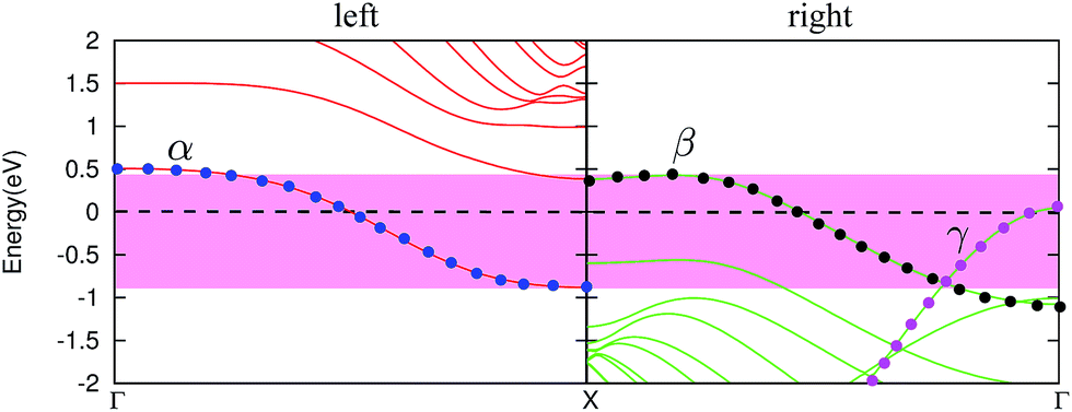
As investigated earlier,32 the C dopants in BNNRs tend to be located at the edges of the ribbon. One typical case is shown in Fig. 1(a), which depicts the schematic configuration of a two-terminal device based on the B-edge substitution (model MB). By substituting the lower N edge atoms or both the upper B edge and the lower N edge, we get other two models MN and MBN (not shown). For comparison, we have also studied the electron transport of the 10-ZBNNR without doping. There is a ∼4.2 eV wide gap around the Fermi level in its transmission spectrum (not shown). This transmission gap originates from the gap with the same size in the band structure which will be shown later. Thus, the current at low bias is zero in a large bias range and it behaves as an insulator.However, this situation is completely changed in the edge-doped ZBNNRs. Fig. 2(a) shows the calculated I–V curves for model MN, MB and MBN. The current increases linearly as a function of the bias voltage starting from zero bias in all three cases, and consequently they behave as a good conductor. The I–V curve is symmetric with respect to the positive and negative biases due to the regular symmetric structures of the device models. Nevertheless, the slopes of the I–V curves are different, indicating different conductances in these cases. We can see that the currents of the MN and MB cases at the same bias are almost equal (with MN slightly larger) while that of MBN is doubled.
 | ||
| Fig. 2 (a) I–V curves and (b) transmission functions for two-terminal devices composed of ZBNNRs with B-edge substitution, N-edge substitution, and both B-edge and N-edge substitutions, respectively. | ||
To investigate the mechanism of such phenomena, we present the transmission functions at zero bias as a function of energy for the three two-terminal device models in Fig. 2(b). Each transmission curve consists of step-like platforms. Most importantly, around the Fermi level, the transmission coefficient is either 1.0 or 2.0, not like in the non-doping case where it is always zero. This leads to metallic behavior in the doped cases. In the MB case, both below and above the Fermi level, the transmission is 1.0, while in the MN case it is 1.0 above the Fermi level and 2.0 below the Fermi level. Interestingly, the transmission function of the MBN case can be regarded as a simple sum of the MB and MN cases in the energy range [−0.8, 0.8] eV. This indicates that the effects of MBN can be considered as a combination of the single MB and single MN. In fact, the current at low bias also satisfies this rule. Another interesting point is that although the transmission below the Fermi level in MB is twice as big as that in MN, the current is almost the same.
In order to understand the differences in the transmission functions of the three cases, we have investigated their band structures (see Fig. 3). For comparison, the band structure of the pristine ZBNNR is also presented in Fig. 3(a), where a band gap of ∼4.2 eV is clearly observed. In the cases of MN and MB, due to the presence of the C chain, the conduction band (labelled with α or blue in Fig. 3(b)) in the MN case and the valence band (labelled with β or black in Fig. 3(c)) in the MB case becomes much more dispersive and the band gap becomes much smaller. Meanwhile, for the substitution of the B atom in the MB case, the C atom is an electron donor (n type doping), thus the empty conduction band in the pristine ribbon becomes partially filled now (see Fig. 3(b)). Effectively, the C doping pulls down the conduction band. For the substitution of a N atom in the MN case, the C atom is an electron acceptor (p type doping), therefore the original fully occupied valence band becomes partially filled (see Fig. 3(c)). Thus, the C doping pulls up the valence band. This changes the ZBNNRs from an insulator into a metal. In MN, besides band β, there is another band (labelled with γ or purple) that slightly crosses the Fermi level and its maximum lies at 0.1 eV. This is why the transmission below the Fermi level in MN is 2.0 and it extends to 0.1 eV above the Fermi level since there are two bands in this energy region. More interestingly, in the MBN case, since the C substitution for B pulls down the conduction band and its substitution for N pulls up the valence band simultaneously, both the α band and the β band are dragged towards the Fermi level and become partially filled. Meanwhile, the γ band also has a tail crossing the Fermi level. Thus, there are two bands in the energy range [0.1, 1.0] eV and three bands in the range[−1.0, 0.1] eV. The number of bands is exactly the value of the transmission in these energy ranges.
 | ||
| Fig. 3 Alignment of band structures of the left and right leads in the symmetric doping cases at zero bias: (a) with no doping; (b) with B edge substitution; (c) with N edge substitution; (d) with both B and N edge substitutions. The Fermi energy is set to 0. | ||
These fantastic band structures originate from the fact that the dopant does not destroy the basic planar structure and the basic band structure. For many other systems, such substitution may greatly change the band structure of the original system. However, in the systems concerned in this work, the C doping acts more like an electron donor or acceptor. Thus, it is regarded as one of the best ways to modulate the performance of ZBNNRs.
Now we look into the origin why the transmission below the Fermi level in the MN case is twice that in the MB case while the current is only slightly larger. Actually, it arises from the relative shift of the band structures of the left and right leads under finite bias. We can use a cartoon to explain this. In Fig. 4, we show the bands of the left and right leads under zero bias (Fig. 4(a)) and a finite bias (Fig. 4(b)) in the MN case. Around the Fermi level there are two bands, β and γ. Thus, we have two transmission channels, namely, from β to β and from γ to γ. At zero bias, the transmission above the Fermi level will be 1 while that below the Fermi level will be 2. In the finite bias (V) case, the left bands will be shifted up by eV/2 while the right bands down by eV/2. In the bias window, namely, the range between the two lines, there are two bands (β and γ) in the left lead, but there is only one band (β) in the right lead. Thus, there is only one transmission channel (from β to β) while the γ channel is blocked in the bias window. Thus the transmission is close to one, which is the same as in the MB case. This is why we have got almost the same current in both the MB and MN cases. This demonstrates that a study of the equilibrium transmission function is not enough and analysing the I–V curve is very important in a device. The current in the MN case is slightly larger than the MB since the transmission platform with height of 2.0 in the MN case extends a little above the Fermi level, which contributes to a transmission of 2.0 in a very small energy range above the Fermi level, and thus contributes to a little fraction of the current.
 | ||
| Fig. 4 Cartoon model of the alignment of band structures of the left and right leads in the MN case around the Fermi level: (a) at zero bias; (b) at finite bias V. β and γ are two bands around the Fermi level. The black dashed line shows the Fermi level and the two green dashed lines indicate the bias window. | ||
The transition of ZBNNRs from an insulator to a metal has also been observed in Yu et. al.’s work, where several rows of BN chains are substituted with C chains and the equilibrium conductances range between 2G0 ( : conductance quantum) and 3G0, depending on whether it is zigzag-edged graphene nanoribbons (ZGNRs) embedded in ZBNNRs or ZBNNRs embedded in ZGNRs.41 We have also studied the cases with several B or N lines replaced by C lines, with the number of B or N lines increasing from 1 to 4. It is found that we can always observe the insulator–metal transition and the equilibrium conductance ranges between 1–3G0 in the MB cases and 2–6G0 in the MN cases. It originates from the facts that more originally empty conduction bands become partially filled in the MB cases due to the C induced electron doping and more fully occupied bands become partially filled in the MN cases due to the C induced hole doping.
3.2 Asymmetric doping
From the study above, we can see that either B edge substitution or N edge substitution changes the nanoribbon into a metal. In a macroscopic situation, when a structure is composed by connecting two metals together, it will still behave as a good conductor. A question naturally arises as to how it will behave when we connect two C doped BN nanoribbons with different substitution scheme. In order to study this problem, we have designed a device as shown in Fig. 1(a). In this model, the B atoms at the upper edge at one side and the N atoms at the bottom edge at the other side are substituted by C atoms, which are both conductors as shown in Fig. 5. Obviously, around the Fermi level, there is an overlapping energy region where there is a band crossing the Fermi level in both regions. However, our study indicates that the current in the whole bias range [−1.5, 1.5] V studied and the transmission in the range [−2.0, 2.0] eV (see Fig. 6(a) and (b)) are exactly zero, which demonstrates that a finite density of states in both leads does not guarantee finite transmission. | ||
| Fig. 5 The alignment of band structures of the left and right leads at zero bias when the C chains of the two regions are located at opposite edges. α, β and γ indicate three bands crossing the Fermi level. The Fermi energy is set to 0. | ||
 | ||
| Fig. 6 The I–V curve (a) and the transmission function (b) in the two doping schemes. Here “edge” means that the C chains are located at opposite edges on the two sides of the junction; “center” means the C chains are located at the center of the ribbon on both sides. | ||
For understanding the origin, in such a situation where two ‘metallic’ materials connected together produce zero conductance and current, a study of the spatial distribution or symmetry of the wave functions is necessary.42 Consequently, we take an insight into how the wave functions of the bands crossing the Fermi level are spatially distributed. The wave function of the conduction band in the MB case and that of the valence band in the MN case at the Γ point are shown in Fig. 7(a) and (b), respectively. We notice that, although the conduction band in the MB case and the valence band in the MN case are overlapping in energy around the Fermi level, their wave functions are well separated spatially. Thus the electron transmission from one lead to the other by these channels is blocked.
 | ||
| Fig. 7 Distribution of the wave functions at the Γ point for: (a) α-band with B-edge substitution; (b) β-band with N-edge substitution; and (c) α-band with B-center substitution; (d) the β-band with N-center substitution. | ||
In order to make the junction conducting, obviously, one way is to tune the wave function distributions so that they are spatially connected. This may be achieved by moving the carbon chains from the edge towards the center. One case is shown in Fig. 1(c). Interestingly, when the carbon chains lie at the center, the current increases almost linearly starting from zero bias (see Fig. 6(a)). In the transmission function, there is a large transmission peak in the energy range [−0.9, 0.4] eV. This range coincides very well with the overlapping energy region in the band structures of the two regions shown in Fig. 8. From Fig. 8 and 5, we find that, no matter whether the C chain lies at the edge or is located at the ribbon center, the bands crossing the Fermi level are always there. Besides changing the dispersion of these bands, the C chains act more like an electron donor or an electron acceptor in the ZBNNRs. From Fig. 7(c) and (d), it can be seen that the wave functions of the bands crossing the Fermi level are all located at the ribbon center. Thus, the electron transmission is permitted now.
 | ||
| Fig. 8 The alignment of band structures of the left and right leads to a zero bias when the C chains of the two regions are both located at the ribbon center. The shadowed area indicates the overlap energy region in both leads. α, β and γ indicate the three bands crossing the Fermi level. The Fermi energy is set to 0. | ||
Another feature in the I–V curve shown in Fig. 6(a) is that negative differential resistance is observed in both the positive and negative bias regions and the peak-to-valley ratio (PVR) in the current in the negative bias region is as large as ∼105, which is much larger than many reported values in other systems.43,44 To gain further insight into the origin of NDR behavior, we plot the transmission spectra as a function of both electron energy and bias in Fig. 9. According to eqn (2), the current through the device is the integration of the transmission T(E, Vb) from μL to μR (the bias window). Since the average Fermi level, which is the average of the chemical potential of the left and right leads, is set as zero, the integration window is actually [−eVb/2, eVb/2].
 | ||
| Fig. 9 Transmission as a function of electron energy and bias. The green dashed cross lines indicate the bias window. | ||
From Fig. 9, we can see how the transmission peak around the Fermi level evolves with the bias. Compared with the zero bias case (see Fig. 6(b)), in the positive bias region, the peak width increases firstly until 0.3 V and then it decreases. In the negative bias region, the peak width decreases monotonously with the bias until 1.3 V. However, the current is determined by the significant integration (SI) region as defined by the region inside the bias window with nonzero bias (indicated by the bright region between the two green dashed lines in Fig. 9). We can see that the width of the SI region increases linearly first until 0.65 V, then it almost keeps unchanged and finally it decreases rapidly in both the positive and negative bias regions. The transmission in this region starts to decrease when Vb ≥ 0.65 V. Thus, the current decreases accordingly and NDR happens. Especially, in the negative bias region, after Vb > 1.3 V which is exactly the overlap energy region width in Fig. 8 at zero bias, due to the upshift (eVb/2 > 0) of bands in the left lead and the downshift (−eVb/2 < 0), the overlap energy region becomes zero. Thus, the transmission and the current are negligibly small, which gives rise to a very large peak-to-valley ratio as shown earlier.
4 Conclusion
In summary, we have investigated the tuning effects of C doping on the electronic and transport properties of ZBNNRs. In the substitution of C for N, the C atom acts as an electron acceptor, thus the fully occupied valence band becomes partially filled. In contrast, in the substitution of C for B, the C atom acts as an electron donor, thus the empty conduction band becomes partially filled. Consequently, the substitution of carbon atoms for either boron atoms or nitrogen atoms always leads to a transition from a semiconductor to a metal. However, in such a metal, there is something special since the conducting channel contributed by the valence band or the conduction band is around the C chain. Thus, in the symmetric doping, we get metallic behavior in the I–V characteristics. Nevertheless, in the asymmetric doping, if the C chain in one doping region is far from that in the other doping region, the conducting channel is disconnected and thus the junction still behaves as an insulator. If the C chain in both region moves to the center of the region along the axial direction, electrons can be transmitted from the conduction band in the region with a B chain substituted to the valence band in the region with a N chain substituted. Thus, it behaves as a good conductor. This demonstrates that the tuning effects of C doping in ZBNNRs depend on the substituted sub-lattice (B or N) and the relative position of the doping site.Acknowledgements
This work is supported by the National Science Foundation of China under Grant nos 11174289, 11347204 and 11104276, the Knowledge Innovation Hefei Center for Physical Science and Technology under Grant no. 2012FXZY004, the Anhui Provincial Natural Science Foundation under Grant no. 1308085QA17, the Fundamental Research Funds for Central Universities, and the Director Grants of CASHIPS. The calculations were performed in the Center for Computational Science of CASHIPS, the ScGrid of the Supercomputing Center and the Computer Network Information Center of the Chinese Academy of Science.References
- K. S. Novoselov, A. K. Geim, S. V. Morozov, D. Jiang, Y. Zhang, S. V. Dubonos, I. V. Grigorieva and A. A. Firsov, Science, 2004, 306, 666 CrossRef CAS PubMed.
- A. K. Geim and K. S. Novoselov, Nat. Mater., 2007, 6, 183 CrossRef CAS PubMed.
- Z. Li, H. Qian, J. Wu, B.-L. Gu and W. Duan, Phys. Rev. Lett., 2008, 100, 206802 CrossRef.
- H. Zeng, C. Zhi, Z. Zhang, X. Wei, X. Wang, W. Guo, Y. Bando and D. Golberg, Nano Lett., 2010, 10, 5049 CrossRef CAS PubMed.
- D. Golberg, Y. Bando, Y. Huang, T. Terao, M. Mitome, C. Tang and C. Zhi, ACS Nano, 2010, 4, 2979–2993 CrossRef CAS PubMed.
- X. Blase, A. Rubio, S. G. Louie and M. L. Cohen, Phys. Rev. B: Condens. Matter Mater. Phys., 1995, 51, 6868–6875 CrossRef CAS.
- K. Watanabe, T. Taniguchi and H. Kanda, Nat. Mater., 2004, 3, 404 CrossRef CAS PubMed.
- Y. Kubota, K. Watanabe, O. Tsuda and T. Taniguchi, Science, 2007, 317, 932 CrossRef CAS PubMed.
- Z. Zhang and W. Guo, Phys. Rev. B: Condens. Matter Mater. Phys., 2008, 77, 075403 CrossRef.
- M. Topsakal, E. Aktürk and S. Ciraci, Phys. Rev. B: Condens. Matter Mater. Phys., 2009, 79, 115442 CrossRef.
- J. Makamura, T. Nitta and A. Natori, Phys. Rev. B: Condens. Matter Mater. Phys., 2005, 72, 205429 CrossRef.
- X. J. Wu, M. H. Wu and X. C. Zeng, Front. Phys. China, 2009, 4, 367 CrossRef PubMed.
- Y. Wang, Y. Ding and J. Ni, Appl. Phys. Lett., 2011, 99, 053123 CrossRef PubMed.
- Y. Ding, Y. Wang and J. Ni, Appl. Phys. Lett., 2009, 94, 233107 CrossRef PubMed.
- F. Zheng, G. Zhou, Z. Liu, J. Wu, W. Duan, B.-L. Gu and S. B. Zhang, Phys. Rev. B: Condens. Matter Mater. Phys., 2008, 78, 205415 CrossRef.
- V. Barone and J. E. Peralta, Nano Lett., 2008, 8, 2210 CrossRef CAS PubMed.
- L. Lai, J. Lu, L. Wang, G. Luo, J. Zhou, R. Qin, Z. Gao and W. N. Mei, J. Phys. Chem. C, 2009, 113, 2273 CAS.
- C.-H. Park and S. G. Louie, Nano Lett., 2008, 8, 2200 CrossRef CAS PubMed.
- M. S. Si and D. S. Xue, Phys. Rev. B: Condens. Matter Mater. Phys., 2007, 75, 193409 CrossRef.
- W. Chen, Y. Li, G. Yu, C.-Z. Li, S. B. Zhang, Z. Zhou and Z. Chen, J. Am. Chem. Soc., 2010, 132, 1699 CrossRef CAS PubMed.
- R.-F. Liu and C. Cheng, Phys. Rev. B: Condens. Matter Mater. Phys., 2007, 76, 014405 CrossRef.
- Q. Tang, Z. Zhou and Z. Chen, J. Phys. Chem. C, 2011, 115, 18531 CAS.
- X. Deng, D. Zhang, M. Si and M. Deng, Phys. E, 2011, 44, 495–500 CrossRef CAS PubMed.
- Y. Xi, X. Zhao, A. Wang, X. Wang, H. Bu and M. Zhao, Phys. E, 2013, 49, 52–60 CrossRef CAS PubMed.
- N. Berseneva, A. Gulans, A. V. Krasheninnikov and R. M. Nieminen, Phys. Rev. B: Condens. Matter Mater. Phys., 2013, 87, 035404 CrossRef.
- S. M.-M. Dubois, X. Declerck, J.-C. Charlier and M. C. Payne, ACS Nano, 2013, 7, 4578–4585 CrossRef CAS PubMed.
- L. Song, X. Zheng, H. Hao, J. Lan, X. Wang and Z. Zeng, Comput. Mater. Sci., 2014, 81, 551–555 CrossRef CAS PubMed.
- H. Park, A. Wadehra, J. W. Wilkins and A. H. Castro Neto, Appl. Phys. Lett., 2012, 100, 253115 CrossRef PubMed.
- M. Chen, Y.-J. Zhao, J.-H. Liao and X.-B. Yang, Phys. Rev. B: Condens. Matter Mater. Phys., 2012, 86, 045459 CrossRef.
- J. Beheshtian, A. Sadeghi, M. Neek-Amal, K. H. Michel and F. M. Peeters, Phys. Rev. B: Condens. Matter Mater. Phys., 2012, 86, 195433 CrossRef.
- S. Tang and Z. Cao, Phys. Chem. Chem. Phys., 2010, 12, 2313 RSC.
- X. Wei, M.-S. Wang, Y. Bando and D. Golberg, ACS Nano, 2011, 5, 2916 CrossRef CAS PubMed.
- N. Berseneva, A. V. Krasheninnikov and R. M. Nieminen, Phys. Rev. Lett., 2011, 107, 035501 CrossRef.
- Z. Liu, Q. Xue, T. Zhang, Y. Tao, C. Ling and M. Shan, J. Phys. Chem. C, 2013, 117, 9332–9339 CAS.
- J. M. Soler, E. Artacho, J. D. Gale, A. Garcia, J. Junquera, P. Ordejon and D. Sanchez-Portal, J. Phys.: Condens. Matter, 2002, 14, 2745 CrossRef CAS.
- K. Burke, J. P. Perdew and M. Ernzerhof, Int. J. Quantum Chem., 1997, 61, 287 CrossRef CAS.
- T. Jeremy, G. Hong and W. Jian, Phys. Rev. B: Condens. Matter Mater. Phys., 2001, 63, 245407 CrossRef.
- M. Brandbyge, J.-L. Mozos, P. Ordejón, J. Taylor and K. Stokbro, Phys. Rev. B: Condens. Matter Mater. Phys., 2002, 65, 165401 CrossRef.
- S. Datta, Electronic Transport in Mesoscopic Systems, Cambridge University Press, Cambridge, England, 1995 Search PubMed.
- H. Haug and A.-P. Jauho, Quantum Kinetics in Transport and Optics of Semiconductors, Springer, Berlin, 1996 Search PubMed.
- Z. Yu, M. Hu, C. Zhang, C. He, L. Sun and J. Zhong, J. Phys. Chem. C, 2011, 115, 10836–10841 CAS.
- X. Zheng, J. Lan, X. Wang, L. Huang, H. Hao and Z. Zeng, Appl. Phys. Lett., 2012, 101, 053101 CrossRef.
- D. H. Zhang, K. L. Yao and G. Y. Gao, J. Appl. Phys., 2011, 110, 013718 CrossRef PubMed.
- A. Pramanik, S. Sarkar and P. Sarkar, J. Phys. Chem. C, 2012, 116, 18064–18069 CAS.
| This journal is © The Royal Society of Chemistry 2014 |