Pallavi B. Patila,
Sawanta S. Malic,
Vijay V. Kondalkara,
Nita B. Pawara,
Kishorkumar V. Khota,
Chang K. Hongc,
Pramod S. Patilb and
Popatrao N. Bhosale*a
aMaterials Research Laboratory, Department of Chemistry, Shivaji University, Kolhapur-416004, India. E-mail: p_n_bhosale@rediffmail.com; Fax: +91-231-2691533; Tel: +91-231-2609338
bThin Film Materials Laboratory, Department of Physics, Shivaji University, Kolhapur-416004, India
cPolymer Energy Materials Laboratory, Department of Advanced Chemical Engineering, Chonnam National University, Gwangju, South Korea
First published on 18th September 2014
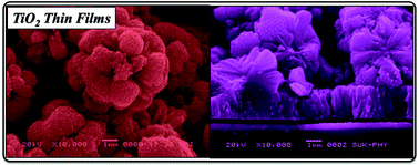
Herein, 3D hierarchical TiO2 microflowers with a well faceted profile and high crystallinity were successfully obtained via a surfactant directed single step facile hydrothermal technique. TiO2 thin films were subjected to different characterization techniques such as UV-Vis-NIR spectrometry, X-ray diffraction (XRD), high resolution transmission electron microscopy (HRTEM), scanning electron microscopy (SEM) and X-ray photoelectron spectroscopy (XPS) for their optical, structural, morphological and compositional analysis. The morphological characterization indicated that the microflowers are made from numerous nanorods growing homocentrically. The length, diameter and degree of aggregation of the nanorods increase rapidly and become aggregated with increase in concentration of CTAB. The effect of CTAB concentration on the microstructure and photoelectric properties of solar cells i.e. open circuit voltage (Voc), short circuit current density (Jsc) and photoelectric conversion efficiency (η%) were investigated under UV illumination. The synthesized 3D hierarchical microflowers can act as a scattering overlayer and 1D nanorod underlayer. 1D nanorods can accelerate the movement of electrons in one direction, while microflowers can scatter light and can enhance the cell performance by light harvesting. An effective improvement in the photoconversion efficiency was observed and lies in the range 0.23% to 3.72%.
Recently, considerable results were achieved with self assembled 1D nanostructure into 3D hierarchical architecture because longer pathway for photon transports, large number of active sites, unique multidimensional hybrid morphology and enhanced light harvesting property.29 Till now, extensive research has been conducted to improve PEC performances with scattering layers in the field of materials chemistry, Y. C. Park et al. synthesized mesoporous TiO2 as a scattering layer by a two step synthesis process with highest efficiency 9.37%.30 J. Jiang et al. demonstrated novel microemulsion-based spherical multihollow TiO2 nanostructures by two step synthesis which acts as scattering overlayer and Degussa P25 underlayer gives 2.33% conversion efficiency.31 9.43% energy conversion efficiency based on DSSC is achieved by H. J. Koo et al. by preparing a nano-embossed hollow spherical TiO2 layer on 20 nm thick TiO2 particulate film.32 S. R. Gajjela et al. reported a photoconversion efficiency of 10.63% for 1 Sun MPT while 10.84% for 0.16 Sun MPT based on DSSC after surface treatment by 40 mM TiCl4 (aq.) solution and screen printing by MPT or NPT of TiO2.33 H. Pang et al. demonstrated the visible range scattering effect of the submicron-sized hollow TiO2 spheres and a bilayered photoelectrode constructed by coating approximately 10 μm thick layer of the hollow TiO2 on top of approximately 10 μm layer of commercial P25 TiO2 which gives conversion efficiency 7.48%.34 All above results based on two step synthesis of double layered/bilayered TiO2 for effective solar cell performance.
Herein we design a novel hierarchical multidimensional hybrid structured TiO2 photoanode by facile one step hydrothermal method. In preliminary the TiO2 thin films were synthesized without CTAB surfactant (sample S1) and in order to investigate the effect of CTAB surfactant on morphology, the concentration of CTAB was varied from 0.025–0.15% (S2–S5). This shows enhancement in the photoconversion efficiency from 0.23–3.72% by providing the direct pathway for photogenerated electrons to flow through TiO2/FTO interface. There is formation of TiO2 microflowers which is act as scattering overlayer and nanorod underlayer. Therefore it is significant to fabricate hierarchical TiO2 photoanode with both high light harvesting and good electron transferring property.
In order to investigate the effect of CTAB on the morphology and photoelectrochemical performance the concentration of CTAB was varied from 0.00%, 0.025%, 0.05%, 0.1% and 0.15% samples designated as S1, S2, S3, S4 and S5 respectively. The reaction temperature and time is kept constant as, 160 °C and 6 h respectively for all deposition.
αhν = a(hν − Eg)n | (1) |
The exponent ‘n’ depends on nature of transition during absorption process. For direct allowed transition n = 1/2 and for indirect allowed transition n = 2. The band gap energy can be estimated by extrapolating straight portion of (αhν)1/2 versus photon energy (hν) shown in inset of Fig. 1 indicating indirect and allowed optical transition.
The band gap energy determined and it varies between 2.89–2.94 eV for samples S1–S5 respectively thus there is no remarkable change is observed in band gap of TiO2 upon addition of CTAB.
Fig. 1 Absorbance spectra of hybrid structured TiO2 microflowers (S1–S5) inset of figure shows optical absorption spectra of the same. |
Sample | Crystallite size (nm) | Lattice parameters (observed) (Å) | Lattice parameters (standard) (Å) | ||
---|---|---|---|---|---|
a | c | A | C | ||
S1 | 39 | 4.5716 | 2.9410 | 4.5925 | 2.9578 |
S2 | 30 | 4.5814 | 2.9513 | ||
S3 | 28 | 4.5895 | 2.9536 | ||
S4 | 27 | 4.5570 | 2.9457 | ||
S5 | 23 | 4.5781 | 2.9500 |
The presence of highly intense, well defined and sharp peaks indicates good crystallinity of the samples. The other peaks observed in XRD which are originated from FTO substrate. The XRD pattern of TiO2 thin films shows no difference in the peak orientation. This indicates that on increase in surfactant concentration there is increase in intensity of reflection. Average crystallite size of TiO2 sample were calculated by using Scherrer's formula shown in eqn (2).
(2) |
The calculated crystallite size of TiO2 for (110) planes are found to be 39, 30, 28, 27 and 23 nm for S1–S5 samples respectively, such crystalline nature suppress the electron hole pair recombination which is beneficial for enhancement in the PEC performance. The * symbol indicates the presence of peak due to FTO substrate.
Fig. 2 X-ray Diffraction (XRD) pattern of hybrid structured TiO2 microflowers in the diffraction angle range (2θ) 20°–80°. |
The basic unit of TiO2 is made up of nanorods as building blocks assembled to form microflowers with length 1.5 μm and diameter 5 μm which is well agreement with SEM results. HRTEM (Fig. 3b) study illustrate that the TiO2 microflowers possess a single crystalline structure of rutile TiO2 with lattice spacing d110 = 3.3 Å indicating the growth along [110] crystal plane with preferred [001] orientation it is well indexed with XRD results.37 The [110] plane is thermodynamically stable plane so; the growth rate along this plane is faster than that of the other planes.38 Fig. 3(b) indicates that the microflower is made from numerous nanorods having average diameter 25 nm. The TEM observation is consistent with the XRD results.
SAED pattern shown in Fig. 3(c) manifests that TiO2 microflowers are not aggregation of small crystallites but made up of monocrystal nanorods growing homocentrically. HRTEM and corresponding SAED pattern confirms single crystalline nature of TiO2 microflowers and the enhanced photoelectrochemical performance can be attributed to improved charge-separation by superior charge transportation through single-crystalline 3D TiO2 microflowers.
Fig. 4 (a) Scanning electron microscopy (SEM) of hybrid structured TiO2 microflowers, inset figure shows low magnification SEM image. (b) Cross sectional view of hybrid structured TiO2 microflowers. |
The SEM study manifests that the shape of microflowers changes significantly from samples S1 to S5. By increasing concentration of CTAB the length, diameter and degree of aggregation of nanorods are increased and formation of microflowers takes place by nanorods growing homocentrically. In case of sample S1 there is formation of incompletely grown microflower while as the surfactant concentration increases well defined microflowers were formed. Such microflowers are made from numerous nanorods display open structure, extended outside and become gradually compact inside.39–43
The cross sectional view of the sample S4 Fig. 4(b) showing that the obtained material is made from two parts, the upper part is made from microflowers with diameter 5 μm while the lower part is made from nanorods nearly perpendicular to FTO with 1.5 μm length. Most of nanorods are densely packed in to bundles. The 1D nanorods can accelerate the movement of electron in one direction while 3D hierarchical microflowers being used as a scattering layer and it can enhance the cell performance by light harvesting. Therefore, double layered structure with scattering layer has been widely used to improve the conversion efficiency of solar cell. It is also observed that there is good connection between microflowers and nanorods which strengthened the interpartical connection offering abundant transfer pathway for photogenerated electrons improving the solar cell performance.
Fig. 6 X-ray photoelectron spectroscopy (XPS) for TiO2 microflowers [a] Survey spectrum of TiO2 [b] core level spectrum of Ti 2p [c] core level spectrum of O1s. |
The presence of carbon at binding energy 284.05 was due to surface contamination when TiO2 thin film was exposed to atmosphere. The core level spectrum of Ti 2p Fig. 6(b) shows peak at binding energy 464.27 and 458.49 eV attributed to Ti 2p1/2 and Ti 2p3/2 respectively. The energy difference between Ti 2p1/2 and Ti 2p3/2 peak was found to be 5.78 eV which corresponds to Ti4+ state of titanium in rutile TiO2 which is well agreement with standard value.44
The high resolution scan of O 1s peak shown in Fig. 6(c) can be deconvoluted into two peaks at binding energy 529.58 and 531.52 eV respectively. The peak at binding energy 529.58 eV corresponds to lattice Oxygen (O–Ti–O) and latter is related to hydroxyl group (OH) adsorbed during transfer.
The photoelectric performance i.e. Fill Factor (FF) and overall light to electric energy conversion efficiency (η%) was calculated by eqn (3) and (4) respectively as follows.
(3) |
(4) |
The solar cell based on hierarchical hybrid structured TiO2 photoanode gives a short circuit current density (Jsc) 0.113 mA cm−2, open circuit voltage (Voc) 383 mV and fill factor (FF) 0.28 yields a power conversion efficiency (η%) is 0.23% for ‘S1’ sample. Effective enhancement in the photoelectrochemical performance is observed with increase in CTAB concentration.
As the CTAB concentration is 0.1% for sample S4 the photocurrent density increases up to 1.255 mA cm−2, Voc is 573 mV and FF is 0.26 giving rise to 3.72% power conversion efficiency. There is sharp increase in photovoltaic performance from sample S3 to S4. This is because in case of sample S3 the unabsorbed light penetrates through nanorods without being scattered for the improvement in PEC performance but for samples S4 the microflowers are assembled with nanorods to form microflowers causes scattering of incident light many times for better photoconversion efficiency i.e. 3.72%.
Scheme 2 Light travelling path in the photoelectrode based on TiO2 nanorods and TiO2 microflowers as a light scattering layer. |
Such improvement in conversion efficiency can be explained on the basis of surface modification by CTAB. The improvement in the energy conversion is due to bilayered structure of TiO2 in which 3D microflowers can act as a scattering overlayer and 1D nanorods underlayer (Scheme 2). The 1D nanorods can accelerate the movement of electron in one direction while 3D hierarchical microflowers being used as a scattering layer and it can enhance the cell performance by light harvesting.45–48 The microflowers forms a compact layer, which favours the accumulation of electrons at the TiO2/FTO interface resulting shifting its potential to higher value.
As the concentration of CTAB increased above 0.1% (sample S5) the rods are densely packed into bundles. Due to formation of densely packed bundles on the surface less scattering of light takes place which results into decrease in the power conversion efficiency. Due to that reason sample S5 posses low photoconversion efficiency i.e. 1.18%. Thus, the effect of surfactant on the photoelectrical performance was summarized in the Table 2.
The series resistance (Rs) and shunt resistance (Rsh) were examined from J–V curve using eqn (5) and (6) respectively as follows,
(5) |
(6) |
The ideal solar cells have Rsh value approaching infinity and Rs near zero. The variation in Rs and Rsh summarized in the Table 2 and Rs and Rsh varies from 471.76 to 2367.6 Ω and 571.42 to 10365 Ω respectively for sample S1–S5. High value Rsh of the material shows no shorts of current in circuit and low value Rs gives high current flow through the circuit. Thus the monotonic increase in open circuit voltage (Voc) due to less resistance to electron transfer and reduction in charge recombination rate. These voltage characteristics largely dependent on shunt resistance (Rsh) and series resistance (Rs).
Electrodes | Voc (mV) | Jsc (mA cm−2) | Vmax (mV) | Jmax (mA cm−2) | FF | η (%) | Rs (Ω) | Rsh (Ω) |
---|---|---|---|---|---|---|---|---|
S1 | 219 | 0.113 | 219 | 0.054 | 0.27 | 0.23 | 2367.6 | 3567.86 |
S2 | 357 | 0.142 | 184 | 0.082 | 0.29 | 0.29 | 1341.18 | 3539.82 |
S3 | 433 | 0.323 | 251 | 0.173 | 0.31 | 0.86 | 1152.00 | 10365.00 |
S4 | 573 | 1.255 | 313 | 0.609 | 0.26 | 3.72 | 471.76 | 571.42 |
S5 | 487 | 0.568 | 301 | 0.279 | 0.30 | 1.18 | 550.00 | 649.77 |
Fig. 8 shows Nyquist plots for samples S1–S5, measured under 0.6 V open circuit voltage in dark and frequency range is from 0.1–105 Hz. The equivalent circuit model fitted to the value is shown in inset of Fig. 8. The equivalent circuit consists of various components: ohmic series resistance [Rs], charge transfer resistance at counter electrode/Electrolyte interface (R1), charge transfer resistance at TiO2 photoanode/electrolyte interface (R2), constant phase capacitance corresponds to R1 and R2 are CPE1 and CPE2 respectively and fitted values are listed in the Table 3
Fig. 8 Electrochemical impendence (EIS) measurement for hybrid structured TiO2 microflowers, inset of the fig shows equivalent circuit employed to fit impedance data. |
Electrode | Rs (Ω cm−2) | R1 (Ω cm−2) | CPE1 (μF) | R2 (Ω cm−2) | CPE2 (μF) |
---|---|---|---|---|---|
S1 | 89.0 | 1410 | 21.2 | 2350 | 18.4 |
S2 | 107 | 4970 | 9.80 | 2630 | 36.4 |
S3 | 98.5 | 8440 | 28.9 | 9440 | 15.5 |
S4 | 85.3 | 1020 | 9.00 | 3770 | 13.8 |
S5 | 173 | 2110 | 29.5 | 4180 | 19.5 |
Electrochemical impendence study reveals that at lower series resistance for sample S4 (85.3 Ω cm−2) which favours the injection of more electrons to the TiO2 photoanode and thereby raising the Fermi level of the TiO2 photoanode and thus shifting its potential to higher value causes enhancement in the photoconversion efficiency.
EIS study suggests that the electric arcs for sample S1–S5 at high frequency region and the electron concentration in TiO2 is low due to frequent recombination, referable to reason that efficiency of TiO2 is limited. The EIS measurement reveals that the impedance of both the electrochemical reaction at counter electrode (R1) and the charge transfer at TiO2 photoanode/electrolyte interface (R2) decreases with surface modification by CTAB. The substantial reduction in resistance mainly ascribed to the improvement in the electron transport. Thus, the sample S4 has R1 = 1020 Ω cm−2 and R2 = 3770 Ω cm−2 which shows lower resistance than that of other samples. Lower the resistance to the flow photogenerated charge carriers adventitious for higher conversion efficiency.
This journal is © The Royal Society of Chemistry 2014 |