
Label-free detection of DNA hybridization using a porous poly-Si ion-sensitive field effect transistor
M. Mahdavia,
A. Samaeianb,
M. Hajmirzaheydaralia,
M. Shahmohammadia,
S. Mohajerzadeh*a and
M. A. Malboobib
aThin Film and Nano-Electronic Lab, Nanoelectronic Center of Excellence, School of Electrical and Computer Engineering, University of Tehran, Tehran, Iran. E-mail: mohajer@ut.ac.ir
bPlant Biotechnology Department, National Institute of Genetic Engineering and Biotechnology, Tehran, Iran
First published on 31st July 2014
Abstract
We report an ultra-sensitive, label-free detection system for DNA hybridization using a porous poly-Si gate ion-sensitive field effect transistor. Various physical and chemical characteristics of the sensor system were optimized, along with parameters affecting the immobilization of a label-free single-strand DNA and the specific hybridization of a complementary sequence on the silicon oxide layer, for quantitative detection down to the femtomole level. X-ray photoelectron spectroscopy (XPS) was employed to investigate the nature of the modifications to the porous layer by covalent bonding. Due to the utilization of nanoscopic pores at the gate region, the Debye screening length is no longer a limitation for macromolecule detection. In addition to its compatibility with the CMOS fabrication process, this sensor is a promising device for the label-free electrical detection of DNA pairs or other biomolecules at low concentrations.
I. Introduction
DNA solid-state sensors have integrated biotechnology with micro/nano-electronic devices. Such devices are being developed and enhanced for a wide range of applications from gene expression studies to food safety strategies.1–4 The use of electrochemical and, more importantly, electrical detectors (the so-called label-free detectors) for signals generated by biomolecules has eliminated the need for labels and massive optical read-out instruments.5,6 These label-free detectors provide a superior alternative to optical detection techniques, which are complex and time consuming and have low sensitivities, high costs and high margins of error.1,7Electrical detection methods for labeled or label-free semiconductor sensing of DNA hybridization can be categorized in the following major groups: ion-sensitive field effect transistors (ISFET),1,8–17 FET Si nanowires (SiNW) or ribbons on the SOI substrate,18–31 EIS capacitors,32–38 capacitive sensors,39–43 cyclic voltammetry44 and TFTs.45–48 All of these methods can detect and quantify biomolecules such as DNA by means of their intrinsic charges or charge transfers during chemical reactions. In the field effect devices, changes in the concentrations of surface charge change the electrical properties of the device, either directly (SiNW sensors) or indirectly (as in EIS or ISFET sensors). In the biotechnology domain, ISFETs have been introduced for the first time as field effect charge sensors based on pH.12,49,50 Investigations into the development of more practical, accurate, robust, cheap, and easy-to-use detection techniques within the above categories are currently being performed.
The electrical detection of single-stranded DNA (ssDNA) and double-stranded DNA (dsDNA) becomes possible by taking advantage of the negative charges of DNA molecules and their slightly changed electrical characteristics when forming non-covalent hydrogen bonds in aqueous solution.6 The potential difference at the electrolyte–solid interface can be influenced by the covalent immobilization of an ssDNA probe on the solid surface. Once recognized by the target DNA, relatively stable H-bonds are formed in stringent conditions, and the change in charge on the solid state can be detected. Ideally, removal of the hybridized DNA by eliminating the stringency factors should restore the charge to its baseline level when only the covalently-attached ssDNA remains on the gate surface.
However, the use of biological and non-biological materials may generate limitations that should be considered for molecular detection. The most important limiting factor affecting the performance of field effect devices emerges from the increased distance of charges from the interface, the so-called Debye screening length. At this distance, the field effect smears out, and charges beyond it cannot be properly detected,24 although this is a function of electrolyte concentration.21 In other words, the sensitivity of the surface to the DNA charges decreases as DNA moves away from the surface.29
The effects of electrolyte concentrations, molecular distances, and orientations on the surface have already been studied.24,28,51 Recent studies suggest that accurate surface modification with linker molecules, thinner gate oxide, and the use of lower concentrations of electrolytes improve the sensing of field effect devices. In our proposed device, we took advantage of porous poly-Si layers to capture and immobilize large numbers of short ssDNA molecules and to overcome such limitations. Porous structures are widely used for biomolecule detection because their larger surface areas inherently lead to signal amplification and compatibility with semiconductor fabrication processes with widely tunable pore sizes.7,52–56
Sensors with high pH sensitivity using the porous gate ISFET have been reported elsewhere.57,58 The effect of various amounts of saline-sodium citrate (SSC) buffer on these sensors has been studied at different steps of surface modification: before and after functionalization with 3-aminopropyltriethoxysilane (APTES), after single-stranded DNA immobilization, and after hybridization.
II. Materials and fabrication
The proposed ISFET was fabricated based on the n-MOS transistor fabrication process, using a channel length and width of 75 and 100 μm, respectively, along with four level masks (Fig. 1). P-type 〈100〉 silicon wafers were degreased and cleaned using the RCA cleaning technique. A 100 nm gate oxide layer was thermally grown, and a 2 μm layer of poly-Si was deposited on the oxide sensitive layer using low pressure chemical vapor deposition (LPCVD). The source and drain active areas and poly-Si layer were doped using a standard phosphorus diffusion furnace. The passivation layer of Si3N4 was deposited using RF-PECVD to achieve 500 nm thicknesses. Drain–source contacts composed of Ti/Au layers were deposited by RF-sputtering. An SU-8 layer with a thickness of 10 μm was utilized to passivate the non-sensitive regions of the transistor (all regions except the poly-Si gate). This layer also acts as a mask for the porous fabrication process. The poly-Si layer was treated by a sequential reactive ion etching (RIE) process to introduce porous structures to the gate region using H2, O2 and SF6 precursors. The formation of the porous layer with the modified reactive ion etching method provides OH sites for the attachment of APTES molecules.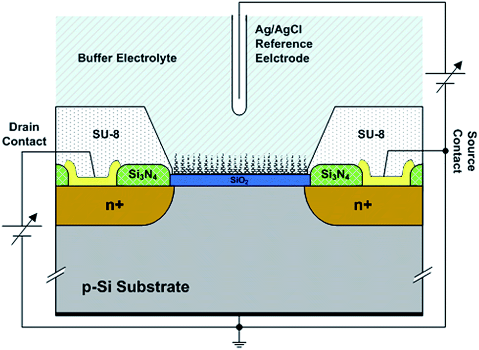 | ||
| Fig. 1 Schematic drawing of the proposed DNA sensor, porous poly-Si gate ISFET sensor, and experimental setup. Experiments were conducted at different steps in the sensor preparation and modification using various concentrations of salts in the hybridization and subsequent washing buffers. | ||
Porous silicon has been used as a substrate for detection in recent decades. Depending on its size, porous silicon can provide a highly effective surface area upon which more molecules can be captured. In the proposed sensor, the porous poly-Si layer above the oxide layer of conventional ISFET leads to an asymmetric capacitance with a noticeable number of OH sites, dramatically enhancing the sensitivity of the sensor. Utilizing the reactive ion etching (RIE) method instead of chemical etching ensures the production of a porous layer fully compatible with the CMOS fabrication process (Fig. 2).
 | ||
| Fig. 2 The porous poly-Si layer above the gate oxide of ISFET: top-view (a) and cross-sectional view (b). The pores penetrate along the poly-Si layer until touching the oxide at the etch stop layer. The mesopores had an average size of 10 nm and were fabricated using reactive ion etching. | ||
III. Experimental
Many different methods of attaching DNA to silicon-dioxide and glass surfaces have been previously described. These include on-chip synthesis of nucleic acids, attachment of pre-synthesized and modified oligonucleotides by means of surface activation using thiol, CN, NH2 and silane, and the use of intermediate molecules, such as glutaraldehyde, and tagged DNA molecules with gold, SH, NH2, biotin or poly-TC tails.4,59–65This report describes a reproducible, simple, efficient and inexpensive protocol that does not require modifications of the molecules involved and can be performed in common laboratories. DNA immobilization methods on plain glass surfaces treated with or without anchoring silanes such as 3-aminopropyltrimethoxy silane (APTES) and GOPS (3′glycidoxypropyltrimethoxy silane) were compared using genomic DNA or oligo-nucleotides cross-linked by exposure to 254 nm UV for 10 min. The attachment was found to be significantly promoted by the use of anchoring groups. However, further experiments were carried out using only APTES because it was easier and simpler to use. The attachments were visually inspected upon exposure to UV after ethidium bromide staining, and precise quantification was performed throughout the experiment. DNA attachment rate and reproducibility were precisely quantified and confirmed by subsequent comparisons between transistor readings (see below).
The surface of the gate was cleaned using a solution of 2 M NaOH and 60% ethanol (v/v) in ddH2O at room temperature for two hours. It was then rinsed six times with ddH2O to remove all traces of NaOH. The device was kept in ddH2O to avoid exposure to air after cleaning. Activation was performed for two hours at room temperature in a solution of 5% APTES and 45% methanol followed by excessive washing, N2 drying and heating for 15 minutes at 100 °C. The pH of the solution was kept at 7–7.5 for surface activation. We achieved a density of 3.5 positive charges per nm2 of gate surface, as shown by a 1 V increase of voltage across the gate.
Two complementary 26-mer oligo-nucleotides were used for perfect matching with each other. The attachment protocol was performed using amino-modified and unmodified oligonucleotides. Even though a higher attachment rate is reported for modified oligonucleotides in the literature,59–61 later experiments were performed with un-modified DNA for simplicity. No significant difference was observed between transistors with attached oligonucleotides or those exposed to 2.30 pmol of oligonucleotides in water. After cross-linking, the unbound DNA molecules were removed by three washes in 0.1% SDS followed by three washes in ddH2O (10 min each, room temperature). The controls were a set of transistors with no DNA attachments that went through all experimental steps. As expected, estimates based on transistor readings indicated an average of 0.5 molecule per nm2 attached to the surface. The possibility of damaged DNA that could severely affect the hybridization rate has not been reported for similar methods59 and remains to be studied. High-resolution XPS analysis at 27 eV pass energy was performed to verify the modification of the porous Si surface with APTES along with the attachment of oligonucleotides (Fig. 3).
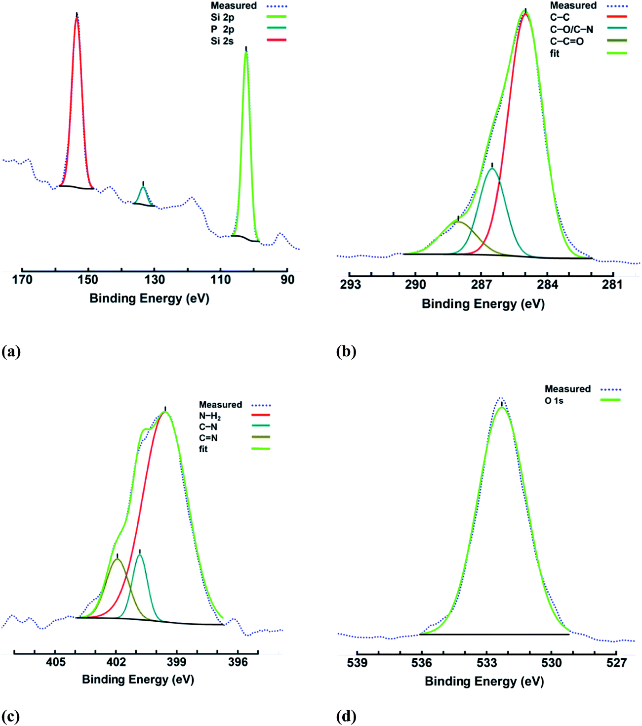 | ||
| Fig. 3 High-resolution XPS spectra of four spectral regions of porous poly-Si functionalized with APTES and cross-linked with oligonucleotides. | ||
The XPS spectra of Si 2p, P 2p and Si 2s, C 1s, N 1s, and O 1s are demonstrated in Fig. 3(a, b, c, and d), respectively; these prove the existence of bonds related to APTES and DNA molecules. Fig. 3(a) shows peaks at 102.4, 133.4, and 153.4 eV, corresponding to SiO2, P 2p, and Si 2s binding energies, respectively. Fig. 3(b) shows the C 1s spectrum with peaks at 285, 286.5, 288 eV, which corresponding to the C–C, C–O or C–N, and C![[double bond, length as m-dash]](https://www.rsc.org/images/entities/char_e001.gif) O bonds, respectively. The spectral region in Fig. 3(c) includes three peaks at 399.5, 400.8, and 401.9 eV with regard to N 1s bindings. The peak at 532.2 eV in Fig. 3(d) results from the contribution of different binding configurations of oxygen molecules.51,66–71
O bonds, respectively. The spectral region in Fig. 3(c) includes three peaks at 399.5, 400.8, and 401.9 eV with regard to N 1s bindings. The peak at 532.2 eV in Fig. 3(d) results from the contribution of different binding configurations of oxygen molecules.51,66–71
The hybridization of oligonucleotides was optimized by several trials for the amount of target DNA, stringency conditions, time and temperature of hybridization and wash buffers.3,4,62,65,72 The limitation of using Na+ in these experiments was minimized by using SU-8 sealing in the device preparation.73 After the immobilized ssDNA quantification process, the devices were cleaned using absolute ethanol and rinsed with ddH2O to remove all traces of alcohol. The devices were incubated in pre-hybridization buffer (2× SSC, 7% SDS) for two hours; 20× SSC is composed of 3 M sodium citrate and 300 mM NaCl. A total of 10 pmol of target DNA per transistor was added in hybridization buffer (2× SSC, 3.5% SDS) and incubated at 55 °C for 10–12 hours with shaking. Temperature optimization yielded the same results as the work of Rose et al.72 suggesting a 17 °C reduction in the calculated Tm. The final concentration of Na+ was 378 mM in hybridization buffer (both SSC and SDS) and 350 mM in the first wash step. Washing steps were carried out using 2×, 1×, 0.75×, 0.5× and 0.25× SSC or ddH2O at room temperature. All the devices including controls underwent the same procedures.
IV. Results and discussion
The DC current characteristics of the sensors were used to indicate the gate surface charge differences. A Keithley 2361 electrical parameter analyzer was used to stimulate and read the voltage and current of sensor terminals. Sensors at different steps of fabrication were examined at drain–source voltages of 0 to 5 V against reference gate electrode voltages of 0 to 5 V. A standard Ag/AgCl reference electrode was used as a reference of electrolyte potential for these experiments. A schematic showing the expected charges on the device during each experimental step is depicted in Fig. 4.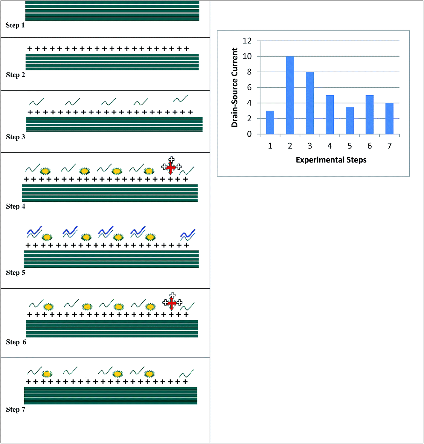 | ||
| Fig. 4 Expected data patterns collected at different experimental steps. Left side: steps 1 to 7 show the possible charges for each experimental step. Black crosses indicate the positive charges due to the introduction of APTES to the surface. Yellow balls show the negatively-charged SDS. The red crosses indicate EDTA molecules. Right side: the expected changes in drain–source current for each step, assuming specific hybridization of DNA molecules at step 5. | ||
Three identical series of sensors, each including at least five devices, were dedicated to three different kinds of DNA probing in every test. Specific target DNA designed for a perfect complementary nucleotide sequence to the covalently-immobilized DNA on the surface was expected to increase the negative charge on the surface after hybridization. A non-specific DNA probe was used to assess the effects of various steps during the measurement procedure on the devices when no hybridization occurred. The third set of sensors was exposed to specific complementary DNA mixed with salmon sperm genomic DNA cleaved to an average size of 500 bp. Equal amounts of specific complementary DNA and Arabidopsis genomic DNA were mixed prior to hybridization (10 pmol of each DNA per device). The purpose of the latter experiment was determine the effect of longer DNA molecules on the porous structures and their physical interaction, as well as to gauge the pairing ability between a specific probe and its target in a pool of unwanted DNA molecules.
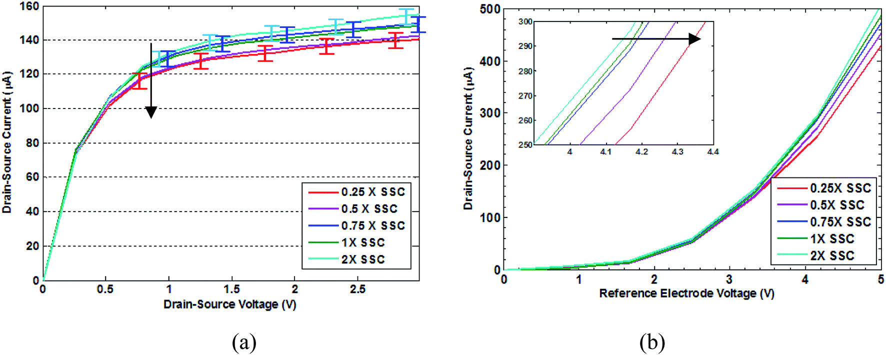
Before functionalization with APTES, all devices were tested in different concentrations of testing buffers (pure water, 0.25×, 0.5×, 0.75×, 1×, and 2× SSC). No significant change was observed in the flat-band potential of the sensors in these solutions before functionalization. The sensors had an average drain–source current of 120 μA. The same experiment was conducted for sensors after functionalization. The results demonstrate that the positive charge of APTES generated a flat-band shift (negative shift in a threshold voltage of approximately 1 V), resulting in an average current of approximately 200 μA, and more sensitivity to the electrolyte concentration. The test steps were repeated after immobilizing probe single-stranded DNA (ssDNA) on the gate surface in each of the DNA hybridization and rinsing buffers. The observed shifts in flat-band voltage (positive shift in threshold voltage of approximately 0.5 V) led to decreases in drain–source current, resulting in an average current of 80 μA. The devices were rinsed, and their current characteristics were measured in 2×, 1×, 0.75×, 0.5×and 0.25× SSC buffers, as well as in water, after the hybridization step. Since the ion concentration in various steps of rinsing is monotonically lowered from 2 to 0.25, one expects to observe a lower ionic strength and, as a result, a monotonic reduction in the measured current. On the contrary, we observed a rise in the measured current, which is related to the detachment of DNA from their complementary strands on the device surface.
The results below show the drain–source current versus drain–source voltage at a reference electrode voltage of 3 V (Fig. 5(a)) and versus reference electrode voltage (Fig. 5(b)). These results indicate that specific (complementary) DNA targets have been hybridized with DNA probe at the surface of the sensor gate. The sequential rinsing steps with SSC buffers leads to the de-hybridization of target DNA, causing the shift in the threshold voltage and peak of the drain current. Washes were begun by rinsing in 2× SSC to observe the hybridization signal of target DNAs while maintaining the bond to probe DNAs (cyan line). The next test, which was carried out in 1× SSC, shows a higher current. Continuing similar tests with 0.75×, 0.5×, and 0.25× SSC rinses lead to the denaturing of target DNAs and, consequently, smaller negative charges and higher currents. No dramatic change in the three last SSC washes was observed. The Id–Vg plots at different steps were used to show changes in the flat-band potential through the different test steps; the arrows point in the general direction of the device current or voltage response to various buffer concentrations.
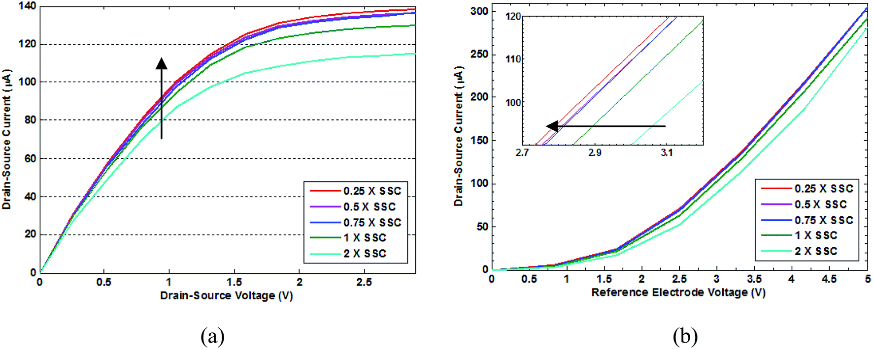 | ||
| Fig. 5 Monitoring changes in current characterisitics resulting from specific DNA hybrization and subsequent sequential washing. (a) Drain–source sensor current versus drain–source voltage. The increase in the DC current characteristics of the sensor shows that most of the hybridized specific DNAs have been denatured at the 0.75× SSC wash step. (b) Drain–source current versus (Ag/AgCl) reference electrode voltage confirming the same results. | ||
Further experiments were conducted to test the binding of non-specific (control) DNA targets. Fig. 6 shows the drain–source current after the hybridization procedure with non-complementary DNA targets. The sequential washing steps were repeated in the same manner as in the previous specific tests. The results of these experiments resemble those obtained from single-strand DNA without the addition of extra DNA in the solutions (non-complementary DNA). A reduction in the current is observed with decreasing buffer concentration, which seems to agree with the corresponding effect of ionic strength and the measured current. It is important to note that in the case of non-specific DNA strands, the behavior of the device is similar to that of a simple pH meter, where the concentration of ions directly affects the measured current. The arrows in Fig. 6 demonstrate the general trend of the device current and voltage with respect to ionic concentrations. For both Fig. 6(a) and (b), a clear contrast with the results presented in Fig. 5 is observed.
 | ||
| Fig. 6 Monitoring changes in current characterisitics resulting from non-specific DNA hybrization and subsequent sequential washing. (a) Drain–source current versus drain–source voltage; the measured transistor current is reduced through washing steps from 2× SSC to 0.25×, in clear contrast with the results of the specific tests. Therefore, the change in the current is essentially a function of the ionic strength of the electrolyte. (b) Drain–source current versus Ag/AgCl reference electrode voltage. The addition of non-specific DNA does not result in any noticeable change in the measured current. | ||
Some studies about field effect sensors show that intrinsic DNA charges are responsible for the detection mechanism.14,33,36 On the other hand, in addition to the intrinsic charges of macromolecules, the ion redistribution of polyelectrolytes has been suggested as another factor controlling charge variation on the surface of sensors in field effect devices.74,75 Regardless of which mechanism controls the surface charge, charge transduction to electrical signal in the EIS structure will be determined by the change in flat-band voltage of the threshold voltage of the system due to the presence or absence of ions at the interface.
The threshold voltage of a sensor can be defined by eqn (1),76
| VT = εref + Δϕlj − ψ0 + χel + ϕF − (ξ + EG/2)/q − (Qss + QB)/Cin |
The capacitance Cin is the total capacitance from the electrolyte–insulator interface to the insulator–silicon interface. In addition to the porous poly-Si and the SiO2 layer under the porous layer, the solid–electrolyte interface is an electrical double layer and is a part of this capacitance. Although the capacitance is non-linear, it can be assumed to be linear in the working range of the sensor. The capacitance is at least 20-times higher than that of oxide (approximately 34 nF cm−2 for our device with 100 nm oxide thickness). This is mainly due to the asymmetric capacitance of the stacked layers of n + doped porous poly-Si and the oxide layers over the semiconductor.
Different surface modification approaches have been explored to enhance the attachment of APTES to the silicon layer.17 In the proposed sensor, the nanoporous structure has been placed on the gate oxide to increase the density of sites for surface attachment. The ideal model has been used to show how the pores with an average size of 10 nm enlarge the effective surface, allowing the small APTES molecules to bind to the surface at higher concentration (Fig. 7).
 | ||
| Fig. 7 The Ideal model for the binding of APTES molecules to the poly-Si pores. The pores have an average size of 10 nm and were created by reactive ion etching. They provide a highly effective surface area for the binding of molecules, thus providing higher sensitivity and overcoming the limitation related to the Debye screening length. | ||
As discussed by Tessier et al., the Debye length in nanoscopic systems is affected by pore size and surface charge. For systems with nanowalls, the Debye length bridges along walls. Thus, in nanoscopic systems, nanopores in spaces encompassed with pore walls are affected by the wall regime instead of the electrolyte regime.77 Higher surface area along with changes in charge distribution and poly-electrolyte concentration due to the porous surface is responsible for the inherent amplification of the sensitive layer.
In order to investigate the effect of APTES layer on flat-band voltage more deeply, the DNA sensors with only APTES layer were examined. The results show a positive shift of approximately 1 V in flat-band voltage due to the positive charges of amino groups. The positively-charged APTES layer seems to compensate for the negative charge on the probe DNA, reducing the electrostatic repulsion between probe and target DNA strands. In addition, a positively-modified surface may increase the local concentration of target oligonucleotides near the surface.33 Functionalization with APTES results in greater charge sensitivity. Ulsu et al. reported that APTES-modified surfaces enhance the pH sensitivity of sensors from 34 mV pH−1 to 52 mV pH−1.11 Bunimovich et al. showed that amine-terminated surfaces lead to an intimate contact of DNA with the surface that can circumvent Debye screening length.21,28 In the literature, a surface charge density of 0.8 C m−2 has been suggested as the upper limit for silicon dioxide attaching charge to the surface; using a lower effective surface charge density would increase the calculated change in surface potential.11,33 Fritz et al. demonstrated a surface coverage of 1 probe per 2 nm2,33 and other studies have reported the immobilization of 4 × 10¹⁵ m−2 oligonucleotide probes on the surface.11 Studies related to the density of the APTES monolayer on textured Si surfaces have indicated an average between 2.1 and 4.2 amine groups per square nanometer.17,51
The data depicted in Fig. 8 show that an increase in the level of SSC for sensors with immobilized ssDNA leads to a positive shift in the flat-band voltage. Independent from the test step, the effect of ion concentrations on the positive flat-band shift has been observed in different steps. The increase in the complexity of the surface leads to a higher chance of Na+ charges affecting the sensitivity of the sensor, as shown by the cyan curve in Fig. 8. Similar mechanisms were observed for the control test. This observation suggests that this sensor can distinguish specific and non-specific binding (Fig. 8, light blue curve). The removal of hybridized DNA leads to a drop in the negative charge of nucleotides, resulting in an increased flat-band voltage due to a decrease in electrolyte at the surface. The clear threshold voltage shift of approximately 300 mV is observed as a hybridization signal (Fig. 8, red curve). Removing the effect of the electrolyte from the hybridization signal shows that higher voltage shifts could be expected at about 500 mV (Fig. 8, dark blue line).
 | ||
| Fig. 8 Change in threshold voltage for the sensor with immobilized ssDNA on the gate. The threshold voltage drops as a result of the increased electrolyte ionic strength (cyan line). Rinsing after specific DNA binding leads to a decrease in the threshold voltage by about 300 mV (red line). The dark blue line shows the change in the threshold voltage due to hybridization. The light blue line shows the result for the non-specific test; the result is similar to that of ssDNA. | ||
The variation in current as a function of surface charge changes can be described using the trans-conductance of the device. Graham's equation, which describes the change in potential at a solid–electrolyte interface for low potential changes and flat surfaces, is no longer useful for this device due to its complex surface structure.

V. Conclusions
In conclusion, we have realized a high-sensitivity, label-free detection device for DNA hybridization based on porous poly-Si gate ion-sensitive field effect transistors. The highly-textured gate region of the field effect transistor leads to a high sensitivity response to low concentrations of complementary DNA species in the measurement solution. Apart from studying the various physical and chemical parameters of the sensor, we have also investigated the effects of specific and non-specific DNA strands on the electrical response of the transistors. Owing to the highly textured gate region, a high detection limit of the order of 1 fM has been recorded for this transistor. This sensor enjoys compatibility with CMOS fabrication processes and seems to be a promising device for label-free electrical detection of DNA pairing or other biomolecules at low concentrations.Acknowledgements
We would like to acknowledge the financial support of Green Biotech Inc. and partial support of the Research Council of the University of Tehran.References
- J. M. Rothberg, et al. An integrated semiconductor device enabling non-optical genome sequencing, Nature, 2011, 475, 348–352 CrossRef CAS PubMed
.
- O. Akhavan, E. Ghaderi and R. Rahighi, Toward Single-DNA Electrochemical Biosensing by Graphene Nanowalls, ACS Nano, 2012, 6, 2904–2916 CrossRef CAS PubMed
- H. Christensen, O. Angen, R. Mutters, J. E. Olsen and M. Bisgaard, DNA-DNA hybridization determined in micro-wells using covalent attachment of DNA, Int. J. Syst. Evol. Microbiol., 2000, 50(Pt 3), 1095–1102 CrossRef CAS PubMed
- A. Kumar, O. Larsson, D. Parodi and Z. Liang, Silanized nucleic acids: a general platform for DNA immobilization, Nucleic Acids Res., 2000, 28, e71 CrossRef CAS PubMed
- T. G. Drummond, M. G. Hill and J. K. Barton, Electrochemical DNA sensors, Nat. Biotechnol., 2003, 21, 1192–1199 CrossRef CAS PubMed
- S. Q. Lud, M. G. Nikolaides, I. Haase, M. Fischer and A. R. Bausch, Field effect of screened charges: electrical detection of peptides and proteins by a thin-film resistor, ChemPhysChem, 2006, 7, 379–384 CrossRef CAS PubMed
- G. Rong, A. Najmaie, J. E. Sipe and S. M. Weiss, Nanoscale porous silicon waveguide for label-free DNA sensing, Biosens. Bioelectron., 2008, 23, 1572–1576 CrossRef CAS PubMed
- S.-J. Kim and E. Yoon, Label-Free CMOS Bio Sensor With On-Chip Noise Reduction Scheme for Real-Time Quantitative Monitoring of Biomolecules, IEEE Transactions on Biomedical Circuits and Systems, 2012, 6, 189–196 CrossRef PubMed
- F. Pouthas, C. Gentil, D. Côte and U. Bockelmann, DNA detection on transistor arrays following mutation-specific enzymatic amplification, Appl. Phys. Lett., 2004, 84, 1594–1596 Search PubMed
- J.-K. Shin, D.-S. Kim, H.-J. Park and G. Lim, Detection of DNA and Protein Molecules Using an FET-Type Biosensor with Gold as a Gate Metal, Electroanalysis, 2004, 16, 1912–1918 CrossRef CAS PubMed
- F. Uslu, et al. Label free fully electronic nucleic acid detection system based on a field-effect transistor device, Biosens. Bioelectron., 2004, 19, 1723–1731 CrossRef CAS PubMed
- T. Sakurai and Y. Husimi, Real-time monitoring of DNA polymerase reactions by a micro ISFET pH sensor, Anal. Chem., 1992, 64, 1996–1997 CrossRef CAS
- K.-S. Song, et al. Label-free DNA sensors using ultrasensitive diamond field-effect transistors in solution, Phys. Rev. E: Stat., Nonlinear, Soft Matter Phys., 2006, 74, 041919 CrossRef
- T. Sakata and Y. Miyahara, DNA Sequencing Based on Intrinsic Molecular Charges, Angew. Chem., Int. Ed., 2006, 45, 2225–2228 CrossRef CAS PubMed
- M. Barbaro, et al. A CMOS, fully integrated sensor for electronic detection of DNA hybridization, IEEE Electron Device Lett., 2006, 27, 595–597 CrossRef CAS
- M. Barbaro, et al. Label-free, direct DNA detection by means of a standard CMOS electronic chip, Sens. Actuators, B, 2012, 171–172, 148–154 CrossRef CAS PubMed
- Y.-L. Wu, J.-J. Lin, P.-Y. Hsu and C.-P. Hsu, Highly sensitive polysilicon wire sensor for DNA detection using silica nanoparticles/γ-APTES nanocomposite for surface modification, Sens. Actuators, B, 2011, 155, 709–715 CrossRef CAS PubMed
- P. Ginet, S. Akiyama, N. Takama, H. Fujita and B. Kim, CMOS-compatible fabrication of top-gated field-effect transistor silicon nanowire-based biosensors, J. Micromech. Microeng., 2011, 21, 065008 CrossRef
- N. Elfström, A. E. Karlström and J. Linnros, Silicon Nanoribbons for Electrical Detection of Biomolecules, Nano Lett., 2008, 8, 945–949 CrossRef PubMed
- C.-P. Chen, et al. Label-free dual sensing of DNA molecules using GaN nanowires, Anal. Chem., 2009, 81, 36–42 CrossRef CAS PubMed
- Y. L. Bunimovich, et al. Quantitative Real-Time Measurements of DNA Hybridization with Alkylated Nonoxidized Silicon Nanowires in Electrolyte Solution, J. Am. Chem. Soc., 2006, 128, 16323–16331 CrossRef CAS PubMed
- A. Gao, et al. Silicon-Nanowire-Based CMOS-Compatible Field-Effect Transistor Nanosensors for Ultrasensitive Electrical Detection of Nucleic Acids, Nano Lett., 2011, 11, 3974–3978 CrossRef CAS PubMed
- A. Vacic, et al. Determination of Molecular Configuration by Debye Length Modulation, J. Am. Chem. Soc., 2011, 133, 13886–13889 CrossRef CAS PubMed
- E. Stern, et al. Importance of the Debye Screening Length on Nanowire Field Effect Transistor Sensors, Nano Lett., 2007, 7, 3405–3409 CrossRef CAS PubMed
- E. Stern, et al. Label-free immunodetection with CMOS-compatible semiconducting nanowires, Nature, 2007, 445, 519–522 CrossRef CAS PubMed
- A. Vacic, et al. Multiplexed SOI BioFETs, Biosens. Bioelectron., 2011, 28, 239–242 CrossRef CAS PubMed
- G. S. Kulkarni and Z. Zhong, Detection beyond the Debye Screening Length in a High-Frequency Nanoelectronic Biosensor, Nano Lett., 2012, 12, 719–723 CrossRef CAS PubMed
- G.-J. Zhang, et al. DNA Sensing by Silicon Nanowire: Charge Layer Distance Dependence, Nano Lett., 2008, 8, 1066–1070 CrossRef CAS PubMed
- J. Li, Y. Zhang, S. To, L. You and Y. Sun, Effect of Nanowire Number, Diameter, and Doping Density on Nano-FET Biosensor Sensitivity, ACS Nano, 2011, 5, 6661–6668 CrossRef CAS PubMed
- F. Patolsky, G. Zheng and C. M. Lieber, Nanowire-Based Biosensors, Anal. Chem., 2006, 78, 4260–4269 CrossRef CAS
- Z. Li, et al. Sequence-Specific Label-Free DNA Sensors Based on Silicon Nanowires, Nano Lett., 2004, 4, 245–247 Search PubMed
- E. Souteyrand, et al. Direct Detection of the Hybridization of Synthetic Homo-Oligomer DNA Sequences by Field Effect, J. Phys. Chem. B, 1997, 101, 2980–2985 CrossRef CAS
- J. Fritz, E. B. Cooper, S. Gaudet, P. K. Sorger and S. R. Manalis, Electronic detection of DNA by its intrinsic molecular charge, Proc. Natl. Acad. Sci. U. S. A., 2002, 99, 14142–14146 CrossRef CAS PubMed
- W.-A. Lai, C.-H. Lin, Y.-S. Yang and M. S.-C. Lu, Ultrasensitive and label-free detection of pathogenic avian influenza DNA by using CMOS impedimetric sensors, Biosens. Bioelectron., 2012, 35, 456–460 CrossRef CAS PubMed
- C. Kataoka-Hamai and Y. Miyahara, Label-Free Detection of DNA by Field-Effect Devices, IEEE Sens. J., 2011, 11, 3153–3160 CrossRef CAS
- K.-H. Lee, J. O. Lee, S. Choi, J.-B. Yoon and G.-H. Cho, A CMOS label-free DNA sensor using electrostatic induction of molecular charges, Biosens. Bioelectron., 2012, 31, 343–348 CrossRef CAS PubMed
- H. Berney, et al. A DNA diagnostic biosensor: development, characterisation and performance, Sens. Actuators, B, 2000, 68, 100–108 CrossRef CAS
- C. Stagni, et al. A Fully Electronic Label-Free DNA Sensor Chip, IEEE Sens. J., 2007, 7, 577–585 CrossRef CAS
- A. Frey et al. A digital CMOS DNA chip, in IEEE International Symposium on Circuits and Systems, 2005, ISCAS 2005 2915 – 2918, 2005, vol. 3, DOI:10.1109/ISCAS.2005.1465237
- M. Schienle, et al. A fully electronic DNA sensor with 128 positions and in-pixel A/D conversion, IEEE J. Solid-State Circuits, 2004, 39, 2438–2445 Search PubMed
- N. Pourmand, et al. Direct electrical detection of DNA synthesis, Proc. Natl. Acad. Sci. U. S. A., 2006, 103, 6466–6470 CrossRef CAS PubMed
- C. Guiducci, et al. Microelectrodes on a Silicon Chip for Label-Free Capacitive DNA Sensing, IEEE Sens. J., 2006, 6, 1084–1093 CrossRef CAS
- F. Wei, B. Sun, Y. Guo and X. S. Zhao, Monitoring DNA hybridization on alkyl modified silicon surface through capacitance measurement, Biosens. Bioelectron., 2003, 18, 1157–1163 CrossRef CAS
- W. Yang, J. E. Butler, J. N. Russell and R. J. Hamers, Interfacial Electrical Properties of DNA-Modified Diamond Thin Films:
![[thin space (1/6-em)]](https://www.rsc.org/images/entities/char_2009.gif) Intrinsic Response and Hybridization-Induced Field Effects, Langmuir, 2004, 20, 6778–6787 CrossRef CAS PubMed
Intrinsic Response and Hybridization-Induced Field Effects, Langmuir, 2004, 20, 6778–6787 CrossRef CAS PubMed - L. Kergoat, B. Piro, M. Berggren, G. Horowitz and M.-C. Pham, Advances in organic transistor-based biosensors: from organic electrochemical transistors to electrolyte-gated organic field-effect transistors, Anal. Bioanal. Chem., 2012, 402, 1813–1826 CrossRef CAS PubMed
- Q. Zhang and V. Subramanian, DNA hybridization detection with organic thin film transistors: Toward fast and disposable DNA microarray chips, Biosens. Bioelectron., 2007, 22, 3182–3187 CrossRef CAS PubMed
- P. Estrela, A. G. Stewart, F. Yan and P. Migliorato, Field effect detection of biomolecular interactions, Electrochim. Acta, 2005, 50, 4995–5000 CrossRef CAS PubMed
- S. Cotrone, et al. Microcantilevers and organic transistors: two promising classes of label-free biosensing devices which can be integrated in electronic circuits, Anal. Bioanal. Chem., 2012, 402, 1799–1811 CrossRef CAS PubMed
- S. Caras and J. Janata, Field effect transistor sensitive to penicillin, Anal. Chem., 1980, 52, 1935–1937 CrossRef CAS
- P. Bergveld, The impact of MOSFET-based sensors, Sens. Actuators, 1985, 8, 109–127 CrossRef CAS
- R. G. Acres, et al. Molecular Structure of 3-Aminopropyltriethoxysilane Layers Formed on Silanol-Terminated Silicon Surfaces, J. Phys. Chem. C, 2012, 116, 6289–6297 CAS
- F. Bessueille, et al. Assessment of porous silicon substrate for well-characterised sensitive DNA chip implement, Biosens. Bioelectron., 2005, 21, 908–916 CrossRef CAS PubMed
- H. Lüth, M. Thust, A. Steffen, P. Kordos and M. J. Schöning, Biochemical sensors with structured and porous silicon capacitors, Mater. Sci. Eng., B, 2000, 69–70, 104–108 CrossRef
- M. J. Schöning, et al. Capacitive microsensors for biochemical sensing based on porous silicon technology, Sens. Actuators, B, 2000, 64, 59–64 CrossRef
- D. Zhang and E. C. Alocilja, Characterization of Nanoporous Silicon-Based DNA Biosensor for the Detection of Salmonella Enteritidis, IEEE Sens. J., 2008, 8, 775–780 CrossRef CAS
- A. Jane, R. Dronov, A. Hodges and N. H. Voelcker, Porous silicon biosensors on the advance, Trends Biotechnol., 2009, 27, 230–239 CrossRef CAS PubMed
- M. Shahmohammadi, N. Zehfroosh and S. Mohajerzadeh, Fabrication of High Sensitivity pH-Meters by Nanoporous Silicon Structures, ECS Trans., 2010, 33, 31–34 CAS
- N. Zehfroosh, M. Shahmohammadi and S. Mohajerzadeh, High-Sensitivity Ion-Selective Field-Effect Transistors Using Nanoporous Silicon, IEEE Electron Device Lett., 2010, 31, 1056–1058 CrossRef CAS
- T. Schüler, et al. UV cross-linking of unmodified DNA on glass surfaces, Anal. Bioanal. Chem., 2009, 395, 1097–1105 CrossRef PubMed
- A. B. Steel, R. L. Levicky, T. M. Herne and M. J. Tarlov, Immobilization of nucleic acids at solid surfaces: effect of oligonucleotide length on layer assembly, Biophys. J., 2000, 79, 975–981 CrossRef CAS
- M. C. Lin et al. in Nanoscale Phenomena, ed. Z. Tang and P. Sheng, Springer, New York, vol. 2, pp. 209–215 Search PubMed
- H. Hirayama, J. Tamaoka and K. Horikoshi, Improved immobilization of DNA to microwell plates for DNA-DNA hybridization, Nucleic Acids Res., 1996, 24, 4098–4099 CrossRef CAS PubMed
- D. Ullien, H. Cohen and D. Porath, The effect of the number of parallel DNA molecules on electric charge transport through ‘standing DNA’, Nanotechnology, 2007, 18, 424015 CrossRef PubMed
- Y.-S. Liu, P. P. Banada, S. Bhattacharya, A. K. Bhunia and R. Bashir, Electrical characterization of DNA molecules in solution using impedance measurements, Appl. Phys. Lett., 2008, 92, 143902 CrossRef PubMed
- H. Gudnason, M. Dufva, D. Duong Bang and A. Wolff, An inexpensive and simple method for thermally stable immobilization of DNA on an unmodified glass surface: UV linking of poly(T)10-poly(C)10-tagged DNA probes, BioTechniques, 2008, 45, 261–271 CrossRef CAS PubMed
- L. S. Shlyakhtenko, A. A. Gall, J. J. Weimer, D. D. Hawn and Y. L. Lyubchenko, Atomic Force Microscopy Imaging of DNA Covalently Immobilized on a Functionalized Mica Substrate, Biophys. J., 1999, 77, 568–576 CrossRef CAS
- X. Zhang, S. Kumar, J. Chen and A. V. Teplyakov, Covalent attachment of shape-restricted DNA molecules on amine-functionalized Si(1 1 1) surface, Surf. Sci., 2009, 603, 2445–2457 CrossRef CAS PubMed
- Y. Han, A. Offenhäusser and S. Ingebrandt, Detection of DNA hybridization by a field-effect transistor with covalently attached catcher molecules, Surf. Interface Anal., 2006, 38, 176–181 CrossRef CAS PubMed
- Z. Lin, et al. DNA Attachment and Hybridization at the Silicon (100) Surface, Langmuir, 2002, 18, 788–796 CrossRef CAS
- G.-J. Zhang, Z. H. H. Luo, M. J. Huang, G. K. I. Tay and E.-J. A. Lim, Morpholino-functionalized silicon nanowire biosensor for sequence-specific label-free detection of DNA, Biosens. Bioelectron., 2010, 25, 2447–2453 CrossRef CAS PubMed
- C.-Y. Lee, et al. Surface Coverage and Structure of Mixed DNA/Alkylthiol Monolayers on Gold:Characterization by XPS, NEXAFS, and Fluorescence Intensity Measurements, Anal. Chem., 2006, 78, 3316–3325 CrossRef CAS PubMed
- K. Rose, J. O. Mason and R. Lathe, Hybridization parameters revisited: solutions containing SDS, BioTechniques, 2012, 33, 54–56 Search PubMed
- P. A. Hammond and D. R. S. Cumming, Encapsulation of a liquid-sensing microchip using SU-8 photoresist, Microelectron. Eng., 2004, 73–74, 893–897 CrossRef CAS
- A. Poghossian, A. Cherstvy, S. Ingebrandt, A. Offenhäusser and M. J. Schöning, Possibilities and limitations of label-free detection of DNA hybridization with field-effect-based devices, Sens. Actuators, B, 2005, 111–112, 470–480 CrossRef CAS PubMed
- M. J. Schöning and A. Poghossian, Bio FEDs (Field-Effect Devices): State-of-the-Art and New Directions, Electroanalysis, 2006, 18, 1893–1900 CrossRef PubMed
- P. R. Barabash, R. S. C. Cobbold and W. B. Wlodarski, Analysis of the threshold voltage and its temperature dependence in electrolyte-insulator-semiconductor field-effect transistors (EISFET's), IEEE Trans. Electron Devices, 1987, 34, 1271–1282 Search PubMed
- F. Tessier and G. W. Slater, Effective Debye length in closed nanoscopic systems: a competition between two length scales, Electrophoresis, 2006, 27, 686–693 CrossRef CAS PubMed
| This journal is © The Royal Society of Chemistry 2014 |