
 Open Access Article
 This Open Access Article is licensed under a Creative Commons Attribution-Non Commercial 3.0 Unported Licence
Textures of Au, Pt and Pd/PdO nanoparticles thermally dewetted from thin metal layers on fused silica
Michael Kracker*,
Wolfgang Wisniewski and
Christian Rüssel
Otto-Schott-Institut, Jena University, Fraunhoferstr. 6, 07743 Jena, Germany. E-mail: Michael.Kracker@uni-jena.de; Fax: +49 03641 948502; Tel: +49 03641 948516
First published on 22nd September 2014
Abstract
This article presents results concerning the basic dewetting procedure of thin metal films on an amorphous substrate. Thin layers of gold, platinum and palladium are deposited on fused silica glass sheets by sputtering. The 14 to 18 nm thick layers of Au, Pt and Pd are dewetted into nanoparticles (NP) at temperatures from 424 to 1600 °C. The morphology of the resulting NP is characterized using scanning electron microscopy (SEM) while crystallographic analyses are performed using electron backscatter diffraction (EBSD). Multiple textures are described to occur and coexist in NP-layers of the respective materials and a temperature dependence of the texture formation in gold NP is proved. The transformation of Pd to PdO and its effects on the texture is also analyzed. It is shown that the cooling rate has an effect on the texture in the case of gold NP as well as on the physical structure of the Pd/PdO NP. Twinning relationships could be described to occur on all samples.
Introduction
Metallic nanoparticles (NP) have been extensively studied and are most frequently produced by chemical methods which include adding organic additives to the system.1–4 In comparison, the thermal dewetting of metallic layers with a thickness in the nm-range into NP to achieve optically active surfaces is performed less often.Dewetting allows the production of large, additive free systems and an interaction between the dewetting metal layer and its substrate which in turn allows a self assembling orientation relationship in the form of a crystallographic texture. Dewetting itself may occur far below the melting point of the metal, e.g. as low as 300 °C for gold,5,6 and has been performed in a number of systems including gold, platinum and palladium. In this article we discuss particle formation effects, morphologies and crystallographic orientations as well as textures independent of the process temperature and the cooling procedure. We also highlight the importance of phase transitions during particle formation while heating as well as cooling. Because gold does not show any phase transitions during annealing, we use comparably produced palladium NP for these experiments which exhibit a pronounced tendency to oxidize during sample preparation.
The faceting of metallic nano particles has been discussed in detail in ref. 7 where AFM-profiles show a facetted particle to be flat on the upper side. It has also been shown that facetted gold NP on sapphire become rounded with increasing temperatures5 which was reported to be accompanied by a loss of the strong 111 texture observed at lower temperatures.5 While a large number of publications feature gold NP e.g.5–11 the literature concerning dewetted NP of Pt and Pd is more manageable.12–23
When it comes to literature describing textures and crystallographic orientations, mainly information concerning gold NP on substrates such as single crystals,5 oxidized Si-wafers8 or glasses6,9 was found by the authors. It has been shown that the gold NP are preferably oriented with a {111}-plane parallel to the substrate surface on oxidized Si-wafers8 and amorphous glasses6,9 indicating this is a self organizing process. If the NP are heated above their melting point on a sapphire substrate, the preferred orientation seems to be lost but the facetted morphology reoccurs if the NP are held at an appropriate temperature for some time.10,11 It was also shown that dewetting is possible on inexpensive materials such as soda-lime-silica-glass. Two superimposed textures were described in correlation with the particle size in experiments where the gold layers were covered by a layer of silica before the dewetting process.9
It is generally accepted that the driving force of thermal dewetting is the minimization of the surface energy in the three phase system; substrate – metallic NP – furnace atmosphere. However, the self-organization into textured layers with defined preferences of certain crystallographic orientations is not really understood. While it seems logical that the fcc-lattice of gold may prefer orientations where the close-packed {111}-layers arrange themselves parallel to the substrate,6,8,9 the loss of such a texture at high temperatures5 and the formation of subtextures where even an obvious relationship to a crystallographic plane is lacking9 remains an open question. These effects, however, should be of interest for all research where dewetted NP are used to induce the growth of layers and nano wires24–26 which possibly show a crystallographic relationship to the seeding NP.
As a number of parameters such as substrate chemistry, substrate microstructure, cooling rates or the atmosphere during annealing may affect this self organization, the current article is aimed at providing a reference for future research by presenting texture analysis of a number of dewetted metal layers on fused silica glass. Fused silica is a suitable material due to its simple chemistry, its high thermal shock resistance and chemical stability as well as its excellent optical properties for the analysis of the plasmonic characteristics of metallic NP in the near UV range down to 200 nm. Additionally, it is available as a high purity material throughout the world. The surface crystallization of fused silica above 1100 °C has recently been studied including texture analysis.27 In the following, we present studies on texture using electron backscatter diffraction (EBSD-) analyses of dewetted layers of Au, Pt and Pd/PdO. In contrast to orientation analyses carried out using X-ray diffraction, EBSD enables to determine the orientation of each individual metallic nano particle from which EBSD-patterns can be obtained and a much more detailed, phase specific texture analysis.
Experimental section
Fused silica glass samples of 8 mm diameter and a thickness of 1.25 mm served as substrates. They were cleaned in an ultrasonic bath for 10 min at 65 °C using a 5% commercial cleaning solution (Tickopur R36). The substrates were subsequently rinsed with deionised water, followed by another two steps of rinsing in deionised water with ultrasonic assistance and finally dried at 110 °C for 1 h.A DC-sputter-system (Edwards Auto 306) with target dimensions of 50 × 50 mm2 for gold (purity 99.99%), palladium (99.95%) as well as a round target of 50 mm diameter for platinum (99%) was used to sputter layers of various thicknesses from 14 to 18 nm. The following parameters were kept constant for all metals during the process: substrate-temperature (21 °C), target-substrate-distance (110 mm), pressure (<10 mPa), voltage (4 kV) and argon pressure (10 Pa). The supplied conditions resulted in a current of 35 mA. The thickness was controlled using a shutter and a film thickness monitor (FTM7, BOC Edwards).
Dewetting was achieved by annealing the samples for 3 h in a muffle furnace at temperatures from 424–1600 °C in air (heating rate 10 K min−1). For a better control of the temperature, all stated annealing temperatures (except 1265 and 1600 °C) were logged during the process using a thermo couple (Ni–CrNi) placed ca. 1 cm vertically above the sample surfaces. After the respective annealing time, the furnace was either switched off, enabling slow cooling, or they were directly removed from the furnace (rapid cooling). The exemplary cooling curved of a slow cooling process from 865 °C is presented in Fig. 1.
 | ||
| Fig. 1 Measured temperature/time correlation of annealing a sample at 865 °C for 3 h followed by the slow cooling process. The rapid cooling procedure is indicated by the dashed line. | ||
The samples were analyzed using a Jeol JSM-7001F equipped with an EDAX Trident analyzing system containing a TSL Digiview 1913 EBSD-camera. EBSD-scans were captured using TSL OIM Data Collection 5.31 and evaluated using TSL OIM Analysis 6.2. The scans were performed using a binning of 4 × 4, a current of about 2.40 nA (measured with a Faraday cup) and a voltage of 20 kV. Only data points with a confidence index (CI) of at least 0.1 were used for texture calculation. All samples were coated with a thin layer of carbon at about 10−3 Pa in order to optimize the surface conductivity for analysis in the SEM. The particle size distribution and particle shape analyses were determined by image processing performed on SEM-micrographs.
Results and discussion
In order to visualize the texture information presented in this article, Fig. 2 schematically shows three orientations of a cubic unit cell towards a substrate and the attributed poles these orientations cause in the 001, 101 and 111 pole figures (PFs). The rings in the illustration visualize the result of a random rotation around which ever direction is perpendicular to the substrate. Finally, the superposition of all textures is presented to show that the central dot (see arrows) is characteristic for only one texture while multiple textures may contribute to a ring in some PFs. | ||
| Fig. 2 Orientations of a cubic unit cell and their poles in the respective pole figures. The rings indicate the result of a random rotation around the respective direction perpendicular to the image plane. | ||
Gold
Gold nano particles are by far the most frequently analyzed system of this topic and textures as well as twinning orientations have previously been described in three different experimental setups.6,8,9 Gold sputtered at a deposition temperature up to 210 °C onto silica has been analyzed in ref. 28, however the NP were not produced by dewetting and information about a crystallographic texture is not presented. The dewetting of Au on fused silica has not been analyzed by EBSD and the result of applying a dewetting temperature high enough to melt the Au layer has not been reported for a sufficiently representative number of particles on any substrate to the best of our knowledge. Hence, multiple Au layers with a thickness of 14 ± 1 nm were annealed at temperatures from 424 to 1102 °C to allow comparability to ref. 6, the comparison to the other metal layers featured in this article and finally the self organization of the layer after heating above the melting point of the metal. Fig. 3 presents SEM-micrographs of the dewetted particles after annealing at (a) 424 °C and (b) 965 °C. The particles are 159 and 113 nm in size and do not show a bimodal size distribution which is in contrast to the results of ref. 7 where dewetted Au layers with a thickness of more than 10 nm showed bimodal size distributions. Dewetting at 424 °C (Fig. 3a) indicates a high degree of faceting which is systematically reduced at the temperature of 965 °C (see Fig. 3b); this is phenomenologically in agreement with ref. 5. | ||
| Fig. 3 SEM-micrographs of gold NP dewetted on glass at (a) 424 °C and (b) 965 °C. Pole figures of textures calculated from EBSD-scans performed on layers dewetted at the stated temperatures visualize preferably occuring orientations. | ||
Hwang and Noh5 recently concluded that the surface energy is responsible for the rounding phenomena and additionally proposed a correlation between the crystal structure of their sapphire substrate and the gold NP. However, the NP described in the present paper were all formed on amorphous SiO2-glass substrates excluding the possibility of a foreign (vaccinating) lattice. The faceting describes a further minimization of the energy and the resulting shape is determined by the Wulff construction and corresponds to a truncated octahedron.7,29 In order to describe the morphology, Barnard et al. calculated the equilibrium shape of gold NPs using a thermodynamic model.30 They found that significant changes in the particle morphology occur before the melting point of the particles is reached. These results were confirmed by Shim et al.31 and the rounding was mathematically also confirmed for copper particles by Nielsen et al.32 The occurrence of twinning is well known in NP of this system and is also explained by a modified Wulff construction.33
The articles discussed above describe the fact that the surface fraction of typical crystal facets, e.g. the 111 face, are reduced with increasing temperature. Hence a shape transformation occurs in addition to a premelting mechanism.32,34 The preferential 111 orientation of the particles is obtained by the formation (dewetting) of an oriented initial metal layer.6 As the temperature increases, the equilibrium shape of the particles is changed, hence the possibility exists, that a particle may tilt by reducing the 111 contact surface,29 and a different crystallographic orientation may be adopted. It may be concluded, that slow cooling may cause the optimal surface at low temperatures to be observed after annealing while fast cooling freezes the morphology observed at high temperatures. However, this argumentation must be performed under consideration of the substrate.35,36
Fig. 3 also shows the 001, 101 and 111 PFs of textures calculated from EBSD-scans performed with a step size of 40 nm covering an area of more than 450 μm2. For the temperature of 965 °C, we present textures from two samples prepared simultaneously (sputtering, annealing at 965 °C, slow cooling, and carbon coating) and a rapidly cooled sample to illustrate the differences which may occur despite identical preparation and to test the effect of the cooling rate. Please note that a very weak 111-texture may be shown in the 111 PF of the rapidly cooled sample if an even more sensitive scale is chosen.
The PFs show that only a 111-texture is observed in the annealed samples up to 718 °C. An additional 001 texture occurs after annealing at 815 and 965 °C. At 965 and 1057 °C, a 101 texture is additionally detected after annealing. The type of the predominantly occurring texture, i.e. “the strongest texture”, may shift between samples and, as a matter of fact, even between different areas on the surface of one sample, hence we will not state a hierarchy. Surprisingly, annealing at 1102 °C, i.e. above the melting point of Au, does not lead to complete destruction of the particle arrangement. However, a crystallographic texture can no longer be detected after annealing above the melting point, which confirms the previous results obtained from only up to 20 particles10,11 for a statistically representative number of NP.
In contrast to lower annealing temperatures, substrate modifications in the form of small depressions or holes were detected after annealing at 1102 °C as shown in Fig. 4. As fused silica is known to crystallize above 1100 °C and the initial crystals have been shown to form depressions in the surface,27 it is possible that these small impressions are tiny surface crystals. However, the nucleation rate would be much higher which could point towards the Au layer or the NP functioning as a nucleating agent at the surface. Alternatively, these depressions could also result from a substrate–NP interaction during dewetting and be visible if the NP observed after melting are not in the positions of the NP formed during dewetting. Twinning as described in ref. 6 and 8 may be observed on all the surfaces analyzed here.
 | ||
| Fig. 4 SEM-micrographs of Au NP dewetted at 1102 °C for 3 h. | ||
These results indicate that the texture formation is temperature dependent but perhaps not substrate dependent for amorphous substrates, as the sole 111-texture previously described on soda-lime-silica-glass6 after annealing at 400 °C corresponds to the data presented here. However, only 111-textures were reported in ref. 8 where Au layers were dewetted and annealing was performed at temperatures from 400 to 1000 °C under controlled atmospheres on oxidized Si-wafers using polymer microspheres in the setup. Although the dominance of the 111 texture is reduced with an increasing annealing temperature, which was also observed using a sapphire substrate,5 a clear 111 texture is still observed after annealing at 1057 °C. Hence the 111 texture is observed throughout the entire temperature range while the 001 texture occurs at 815 and 965 °C and the 101 texture occurs at 965 and 1057 °C.
As most samples were cooled slowly, it is impossible that the textures formed solely during cooling because if that were the case all the samples should feature the same textures. At the same time the observation of facetted as well as rounded particles clearly shows that the applied “slow” cooling process is still fast enough to freeze the high temperature morphology of the particles. The absence of a texture after heating above the melting point may be seen as proof that the NP contributing to the textures measured by EBSD are too large to be significantly affected by the melting point reduction observed in very small NP.37 Additionally, it clearly proves that texture formation is caused by a self organization during dewetting which does not occur during the solidification of a melt.
The particle size distributions of the surfaces represented by the SEM-micrographs in Fig. 3a and b are presented in Fig. 5 and are fitted by a Gaussian distribution. The (SEM projection) area of each particle was determined and the diameter of the corresponding area equivalent circle is calculated. The mean particle diameter is 159 ± 58.5 nm at 426 °C and decreases to 113 ± 38 nm after the heat treatment at 965 °C. This effect can be explained by the Rayleigh instability, where elongated particles disintegrate into several smaller particles at higher temperatures and a decrease of the particle size should occur accompanied by an increase of the particle number and consequently a more narrow size distribution. It should be noted that these micrographs only show a projection of the particles, hence a statement about the three-dimensional shape cannot be made here.
 | ||
| Fig. 5 Equivalent circle diameter of gold NP formed by dewetting at 426 and 965 °C for 3 h. | ||
As statistical analyses or the particle size distribution were not given in ref. 6 and 9 we would like to amend this here: a bimodal size distribution cannot be detected in the SEM-micrographs of the samples featured in both articles.
The circularity of a particle can be mathematically defined by a feret ratio where the maximum and minimum diameter of a particle is determined and the related ratio is calculated.6 Hence a value of “1.0” is equivalent to a circle while a value of “0.0” corresponds to an infinitely long string. A detailed analysis of the particle shape in Fig. 6 using the ferret ratio exhibits a log-normal distribution. Annealing at 426 °C for 3 h results in a maximum at 0.76 while increasing the temperature to 965 °C shifts the maximum to 0.88 and narrows the distribution.
 | ||
| Fig. 6 Feret ratio of gold NP formed by dewetting at 426 and 965 °C. | ||
This confirms the visual impression that the particles become increasingly rounded at higher temperatures which has also been reported for gold NP dewetted on crystalline sapphire.5 The fits shown in Fig. 5 are negative skew lognormal distributions. In order to perform a sufficient coverage, the independent variable x = (x − 1) is assumed for the equation of the lognormal distribution.
Platinum
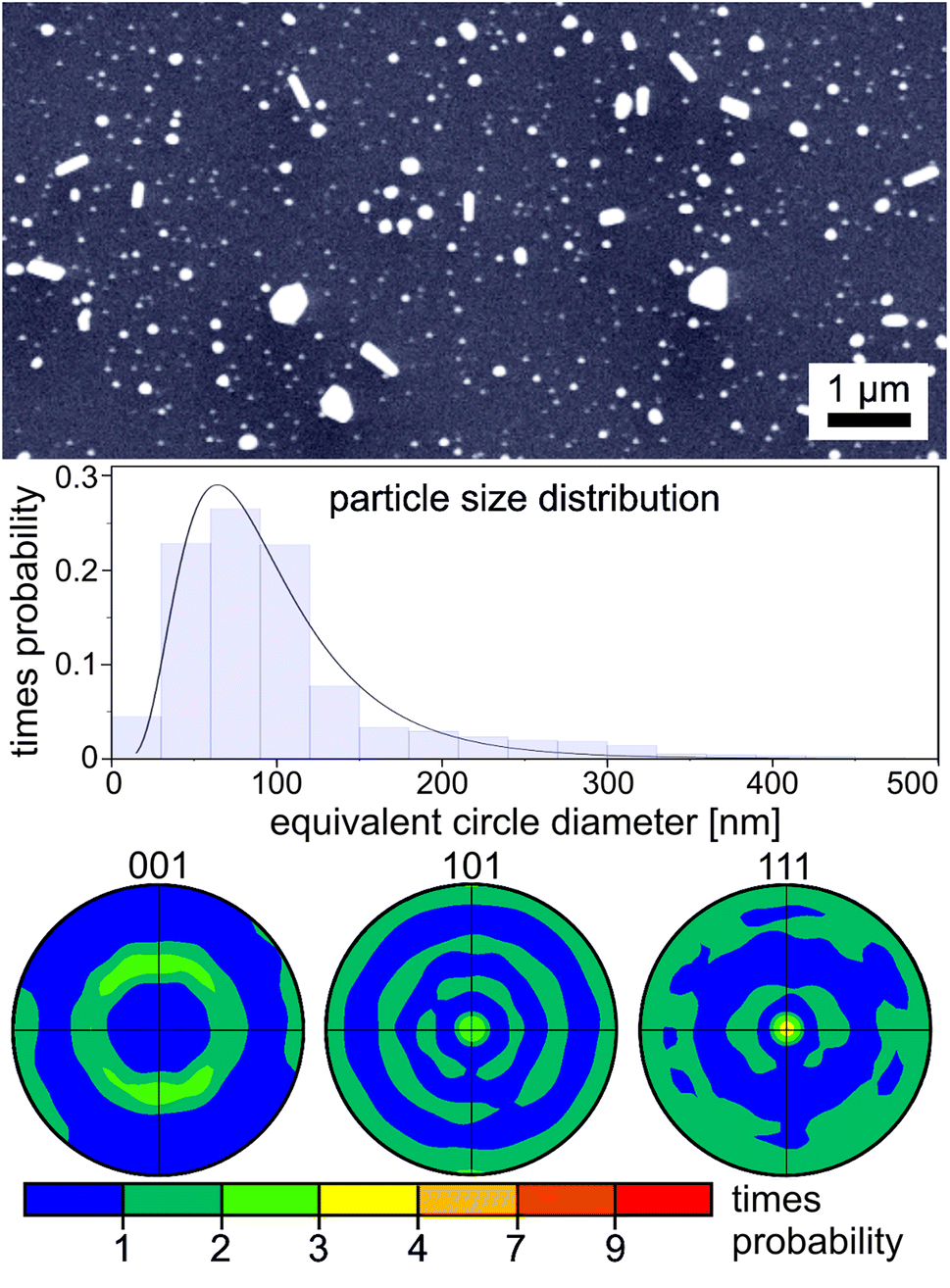
Platinum nano particles are interesting because they combine the catalytic properties of Pt with a relatively large surface. They may also be used as an etch mask. However, Pt and Si form alloys of multiple compositions with melting points down to 830 °C and SiO2 may be reduced by H2 (ref. 38) or an electrical current in a glass melt39 to provide the alloying component. The thermal dewetting of Pt on Si with a natural oxide layer has been studied for layers from 1.5 to 15 nm deposited by electron beam evaporation and annealed at 400 to 1000 °C for only 30 to 240 s with a focus on NP morphology.12 Increasing the annealing time led to larger particles in a narrower size distribution.12,40 The formation of PtSi-phases and nano wire growth was observed when annealing Pt-layers on Si wafers.12,13 In addition, interactions with other substrates are not uncommon.41Due to the lack of a reducing agent, PtSi alloys should not play a role in the experiments performed here. Additionally, all Pt1Si1 phases known to the authors are not cubic and hence their EBSD-patterns would not be reliably indexable as metallic Pt. Dewetting sputtered Pt layers of 14 nm at 965 °C for 3 h led to the Pt NP presented in the SEM-micrograph of Fig. 7 which show a regular log normal size distribution if the circle diameter in the SEM-micrograph is analyzed as illustrated below. The centre of mass is 84.0 nm −34.1 and + 57.5. Some of the large particles show faceting into triangles or irregularly shaped hexagons as well as rods. The rods protrude from the surface and hence might also be described as whiskers or nano wires, making a statement towards true particles sizes problematic for these samples. Fig. 7 also presents 001, 101 and 111 PFs of textures calculated from an EBSD-scan covering 4500 μm2 with a step size of 100 nm. The PFs show a double texture where crystal orientations with either a {101} or a {111} plane parallel to the substrate surface preferably occur. A 100 texture is not indicated. Attempting to perform a size-dependent texture analysis comparable to that presented in ref. 9 only showed that reliable data points with a low image quality (<30%) show the same texture information as the entire scan. 111-twinning in the form of two orientations within one NP sharing a common {111} plane was also detected in these samples. Annealing Pt above the melting point of 1772 °C is not possible using fused silica substrates because the glass crystallizes to high-cristobalite above 1100 °C which in turn melts at 1713 °C.
 | ||
| Fig. 7 SEM-micrograph of Pt NP dewetted at 965 °C and pole figures of a texture calculated from an EBSD-scan performed on the surface. The elongated particles are nano rods protruding from the surface. | ||
Palladium/palladium oxide
Palladium in the form of NPs, thin layers and foams are of notable interest in materials science due to their interaction with hydrogen14,15 and their catalytic activity with respect to various chemical reactions.42–45 Therefore the material is used as a catalytic agent, in gas purification systems and hydrogen sensors.46–48 Pd NP have special optical (plasmonic) properties which change significantly if the particles are oxidized to palladium oxide.16 Pd is not inert during annealing in air but oxidizes to PdO above 258 °C and starts to decompose back to metallic Pd at temperatures above 775 °C (both temperatures correspond to the DTA onset).16 The crystal structure changes from cubic to tetragonal during oxidation49 which enables to identify the individual phases using EBSD. The oxidation of Pd to PdO has been studied on a Pd film under a controlled atmosphere.50 PdO is also reduced in the presence of hydrogen18 meaning an oxidized layer may be converted to metallic palladium at room temperature.19,20 These properties of palladium are of interest for NP research and preparation in general. Hence, the effect of the phase transition at higher temperatures can be studied at room temperature. In addition, this phase transition can be reversed at room temperature by purging with H2. The size dependent kinetics of Pd-hydration have been studied on nano structured materials,51 thin films52 and nano particles.53–55 Michalak et al. described the possibility of thermally induced spinodal dewetting in thin Pd layers.21 However, those experiments were performed in ultra high vacuum (UHV) which completely suppresses the oxide phase. Moreover, Mizsei et al. heated thin Pd layers on glass substrates at atmospheric conditions up to 600 °C and observed no dewetting but the formation of PdO as well as large accumulations of material in the film.22 After adding hydrogen at 500 °C, a preferred 111 orientation of palladium was described.23 While the presented structures resemble those shown in ref. 20, it would seem the temperature was not high enough to produce completely separated particles.In a first step we present results obtained from samples prepared by a non-chemical dewetting procedure at 965 °C and ambient conditions. As the oxidized species of palladium decomposes to metallic Pd between 775 and 800 °C,15,17 the use of hydrogen can be omitted during dewetting. Due to the oxidation behavior of Pd, an effect of cooling rates on the PdO formation during cooling may not be neglected and the applicability of texture analysis after flushing with H2 gas must be analyzed. Hence comparable samples with a Pd layer thickness of 18 nm were annealed at 965 °C for 3 h after which one sample was directly removed from the furnace, causing a high cooling rate of more than 800 K min−1, while the other was left in the furnace to cool slowly. Both samples were then coated with carbon, analyzed by EBSD, flushed with H2 and reanalyzed by EBSD. The acquired results are presented in Fig. 8 along with EBSD-patterns of Pd and PdO.
 | ||
| Fig. 8 SEM-micrograph of Pd NP dewetted from a 18 nm thick Pd film by annealing for 3 h at 965 °C followed by fast cooling. EBSD-patterns of Pd and PdO are presented in the insets. EBSD-scan 1 was performed directly after annealing while scan 2 was performed after the sample was additionally flushed with H2 gas for 15 min. Textures of Pd and PdO calculated from the scans 1 and 2 as well as comparable scans obtained from a slowly cooled sample flushed with H2 for 30 min are presented below along with the number of reliable data points (CI > 0.1) contributing to the respective texture. | ||
EBSD-pattern acquisition was very difficult from the unpurged, quickly cooled sample so that only ca. 400 data points were of sufficient quality (confidence index CI > 0.1) in a scan of almost 200![[thin space (1/6-em)]](https://www.rsc.org/images/entities/char_2009.gif) 000 patterns. While this is within the error margin of the indexing procedure, it was possible to locally obtain high quality EBSD-patterns of Pd from this surface. The latter cannot be said for PdO. Hence, the corresponding 111 texture of Pd indicated by the PF is probably real although not representative while the reliability of the PdO texture must be questioned altogether. After flushing with H2, the NP from the same area provided well indexable EBSD-patterns of Pd indicating clear 001 and 111 textures while the number of patterns attributed to PdO with a CI > 0.1 is again within the error margin.
000 patterns. While this is within the error margin of the indexing procedure, it was possible to locally obtain high quality EBSD-patterns of Pd from this surface. The latter cannot be said for PdO. Hence, the corresponding 111 texture of Pd indicated by the PF is probably real although not representative while the reliability of the PdO texture must be questioned altogether. After flushing with H2, the NP from the same area provided well indexable EBSD-patterns of Pd indicating clear 001 and 111 textures while the number of patterns attributed to PdO with a CI > 0.1 is again within the error margin.
The increase of the ability to acquire EBSD patterns after flushing may indicate that the NP initially showed a core–shell structure of Pd surrounded by a thin PdO layer despite the high cooling rate. The combination of both crystal lattices (Pd and PdO) within the information volume of EBSD may lead to pattern superposition (e.g. at grain boundaries) or prevent the formation of an EBSD-pattern as may be assumed here.
The presence of PdO despite rapid cooling and its influence on the optical properties of the nanoparticles was already shown in ref. 48.
The sample cooled slowly showed well indexable EBSD patterns of PdO after annealing while Pd was not detected reliably. After flushing with H2, the NP on the surface failed to produce a percentage of EBSD-patterns comparable to that obtained from the quickly cooled sample (only 0.03%). However, the 1796 reliably indexed EBSD-patterns of Pd in the scan indicate the same coexistence of a 001 and a 111 texture which was also observed in the quickly cooled sample after flushing with H2. As the optical properties of this sample indicate a reduction of PdO to Pd and only a negligible amount of patterns is indexed as PdO by EBSD, the question arises why EBSD-patterns cannot be obtained from most particles. This problem was detected on numerous samples cooled slowly after annealing at various temperatures.
As it is possible to obtain EBSD-patterns of high quality from a few NPs, errors due to sample preparation, i.e. the thickness of the carbon coating, can be neglected. Additionally, the experiments performed on the quickly cooled samples show that flushing with H2 after carbon coating led to the reduction of PdO in a comparably prepared sample. The detailed SEM-micrographs of Pd NP resulting from slow and rapid cooling after annealing at 965 °C and purging with H2 presented in Fig. 9 show a pronounced morphological difference between the particles. The particle shape is “rugged” after the particle oxidized completely and formed PdO of higher volume20 during the slow cooling process, see Fig. 9a. In contrast, the rapidly cooled NP in Fig. 9b are rounded, again implying that any oxidation during rapid cooling only forms a thin shell of PdO on a core of Pd as already outlined above. Hence the structure of a quickly cooled Pd/PdO NP is quite different from that of a slowly cooled Pd/PdO NP even after being flushed with H2. However, a more detailed analysis of this aspect is beyond the scope of this article.
 | ||
| Fig. 9 SEM-micrographs of dewetted Pd particles on the glass surface (a) cooled slowly and (b) cooled rapidly. | ||
Hence it must be noted that cooling rates affect the structure of the NPs in this system and possibly the texture formation. It is probable that the phase transformations of Pd to PdO and vice versa have no effect on the texture of quickly cooled NP because they were never fully oxidized (PdO was not reliably detected by EBSD on the quickly cooled sample in contrast to the slowly cooled sample). Please note that none of the PFs of PdO allow any certain conclusion on the possible textures of PdO because the two cubic textures of Pd allow at least six tetragonal PdO textures which in turn would probably not show an elevated probability of any orientation and hence remain unnoticed. A similar cubic-tetragonal transition also occurs during cooling after the surface crystallization of fused silica.27
A temperature series was performed to allow a comparison with the results of gold presented above. These samples were always rapidly cooled in order to minimize oxidation and flushed with H2 for at least 15 min to obtain metallic Pd as the results of Fig. 8 showed that even rapid cooling cannot prevent the formation of a thin oxide layer. The resulting SEM-micrographs in Fig. 10 show that the palladium has a much smaller temperature window in which dewetting occurs. After 3 h at 767 °C, the layer is not dewetted and contains star shaped cracks which were also observed in ref. 20. Well separated particles are observed after annealing at 876 °C for 3 h with an additional substructure between the particles, see arrows, which probably results from the irregularly shaped layer residue. These substructures are no longer visible after annealing at 965 °C. Pd could not be detected by EDX on the surface of the sample annealed at 1256 °C where the SEM-micrograph only shows depressions and a crack. This temperature was chosen to see what happens during the dewetting procedure if the substrate crystallizes during annealing but below the melting point of the metal. As the sample is fully crystallized here, these depressions cannot be small cristobalite nuclei as proposed in Fig. 4 but probably indicate locations where the Pd NP interacted with the substrate after dewetting but before disappearing, probably by evaporation. The absence of Pd was also observed for a sample annealed at 1600 °C (not shown), i.e. above the melting point of Pd, but there was no trace of the depressions shown in Fig. 11. Please note that the cracks in crystallized fused silica form due to the phase transformation between 200 and 275 °C,27 i.e. liquid Pd cannot flow into the cracks, again pointing towards an evaporation of Pd.
 | ||
| Fig. 10 SEM-micrographs of rapidly cooled Pd-films annealed at the stated temperatures for 3 h. | ||
 | ||
| Fig. 11 Temperature series of Pd layers annealed at the stated temperatures for 3 h. SEM-micrographs feature surfaces from which EBSD-patterns could not be obtained. 001, 101 and 111 PFs of textures calculated from EBSD-scans performed on NPs dewetted from the Pd layers. | ||
The particle size distributions corresponding to Fig. 10 are presented in Fig. 11 where bimodal Gaussian distributions are clearly indicated. At 876 °C, the determined mean particle sizes of the respective peaks are 45.6 ± 28.6 and 185 ± 48.0 nm while at 965 °C they are 88.8 ± 74.4 and 331.0 ± 89.0 nm. A bimodal size distribution was also detected for 5 nm thick Pd layers dewetted on fused silica.16 It seems logical that the continuously dewetting layer residue leads to the smaller particle species in the bimodal size distribution. Coalescence and Ostwald ripening shift this bimodal distribution to larger particle sizes as the atomic mobility is increased by annealing at the higher temperature. However, the exact reason of the thin layer residue is not yet fully understood because such thin structures should have dewetted long before the large particles in the layer were formed. It must be noted, that a statistical analysis of the figures presented in ref. 21 where oxidation was prevented during annealing does not show a bimodal size distribution.
Hence two different dewetting mechanisms may exist: when the layer reaches the dewetting temperature, it is heavily disturbed due to the volume expansion during oxidation and the subsequent volume decrease due to the thermal reduction. The resulting layer morphology containing the star shaped holes (see Fig. 10) is not comparable to the hole formation in a gold layer.56 Please note that dewetting Pd in a vacuum,21 i.e. without the phase transformation, leads to dewetting morphologies similar to the spinodal dewetting of gold. Hence material accumulations may already exist in the oxidized and reduced system before the actual (spinodal) dewetting begins.22
Fig. 11 also presents texture information on the Pd-layers dewetted at 876 and 965 °C, EBSD-patterns could not be obtained from the sample annealed at 767 °C. The PFs of the samples annealed at 876 and 965 °C both show 001 and 111 textures while a 101 texture is not detected. 111-twinning of Pd was observed in all EBSD-scans of H2-flushed samples featured in this article.
Conclusion
The thin films of all studied materials show a dewetting of the metallic film into metal nano particles at high temperatures. The experiments focused on the crystallographic and morphological behavior of the resulting particles as a function of temperatures, cooling rates and chemical phase transitions during preparation. It was shown that the cooling rate may not be neglected in the cases of Au and Pd where temperature dependent particle forming/aging mechanisms were observed. Interactions with the substrate at high temperatures are implied in all cases.Because Au, Pt, and Pd are all fcc materials, it is of no surprise to find the 111-texture and the 111-twinning in the NP. The 001- and 101-textures, on the other hand, have not been described before and do not occur in the dataset of the previously analyzed Au particles.6 For both orientations, a crystallographic axis is oriented parallel to the substrate surface. At 965 °C, all three textures were detected in Au NP while only the 111 and 101 textures were detected in Pt NP and only the 111 and 001 textures were detected in Pd NP. Particle size dependent textures were not detected after dewetting on fused silica. 111-twinning was observed in the metallic NP of all metals analyzed here.
In the case of Au, it was shown that any texture is lost if the metal is melted during annealing. Comparable results could not be obtained for Pd and Pt due to evaporation or the melting of the substrate, respectively.
Gold NP show a rounding in the particle shape with increasing dewetting temperature on the amorphous substrate in agreement to the literature. In contrast to gold, the dewetting of Pd NP leads to a bimodal size distribution caused by a different dewetting mechanism. Pd NP also show faceting and the morphology is affected by the cooling procedure due to the time and temperature dependent phase transition which also affects the ability to acquire EBSD-patterns. The observed structural modification implies a significantly different NP structure.
Nano rods were observed after dewetting Pt on fused silica.
Acknowledgements
The authors would like to thank T. Zscheckel for a number of SEM-micrographs featured in this article and W. Seeber for his support. This work is supported by the DFG “Deutsche Forschungsgemeinschaft” (Se 698/10-1, Se 698/10-2 and Ru 417/14-1).References
- S. Guo and E. Wang, Anal. Chim. Acta, 2007, 598(2), 181 CrossRef CAS PubMed.
- M. Grzelczak, J. Pérez-Juste, P. Mulvaney and L. M. Liz-Marzán, Chem. Soc. Rev., 2008, 37(9), 1783 RSC.
- R. Sardar, A. M. Funston, P. Mulvaney and R. W. Murray, Langmuir, 2009, 25(24), 13840 CrossRef CAS PubMed.
- K. Na, Q. Zhang and G. A. Somorjai, J. Cluster Sci., 2014, 25(1), 83 CrossRef CAS.
- J. S. Hwang and D. Y. Noh, J. Korean Phys. Soc., 2013, 62(1), 6 CrossRef CAS.
- C. Worsch, M. Kracker, W. Wisniewski and C. Rüssel, Thin Solid Films, 2012, 520(15), 4941 CrossRef CAS PubMed.
- C. M. Müller, F. C. F. Mornaghini and R. Spolenak, Nanotechnology, 2008, 19(48), 485306 CrossRef PubMed.
- M. Bechelany, X. Maeder, J. Riesterer, J. Hankache, D. Lerose, S. Christiansen, J. Michler and L. Philippe, Cryst. Growth Des., 2010, 10(2), 587 CAS.
- C. Worsch, W. Wisniewski, M. Kracker and C. Rüssel, Appl. Surf. Sci., 2012, 258(22), 8506 CrossRef CAS PubMed.
- H. Sadan and W. D. Kaplan, J. Mater. Sci., 2006, 41(16), 5099 CrossRef CAS PubMed.
- H. Sadan and W. D. Kaplan, J. Mater. Sci., 2006, 41(16), 5371 CrossRef CAS.
- S. Strobel, C. Kirkendall, J.-B. Chang and K. K. Berggren, Nanotechnology, 2010, 21, 505301 CrossRef PubMed.
- P. K. Sekhar, S. N. Sambandam, D. K. Sood and S. Bhansali, Nanotechnology, 2006, 17(18), 4606 CrossRef CAS PubMed.
- T. B. Flanagan and W. A. Oates, Annu. Rev. Mater. Sci., 1991, 21(1), 269 CrossRef CAS.
- S. Kishore, J. Nelson, J. Adair and P. Eklund, J. Alloys Compd., 2005, 389(1–2), 234 CrossRef CAS PubMed.
- M. Kracker, C. Worsch and C. Rüssel, J. Nanopart. Res., 2013, 15(4), 1594 CrossRef.
- G. Bayer and H. Wiedemann, Thermochim. Acta, 1975, 11(1), 79 CrossRef CAS.
- J. Han, G. Zhu, D. Y. Zemlyanov and F. H. Ribeiro, J. Catal., 2004, 225(1), 7 CrossRef CAS PubMed.
- J. I. Avila, R. J. Matelon, R. Trabol, M. Favre, D. Lederman, U. G. Volkmann and A. L. Cabrera, J. Appl. Phys., 2010, 107(2), 23504 CrossRef PubMed.
- M. Kracker, C. Worsch and C. Rüssel, Mater. Lett., 2013, 110, 114 CrossRef CAS PubMed.
- W. D. Michalak, J. B. Miller, C. Yolcu and A. J. Gellman, Thin Solid Films, 2012, 522, 473 CrossRef CAS PubMed.
- J. Mizsei, P. Sipilä and V. Lantto, Sens. Actuators, B, 1998, 47(1–3), 139 CrossRef CAS.
- J. Mizsei, L. Pirttiaho, M. Karppinen and V. Lantto, Sens. Actuators, B, 2000, 65(1–3), 195 CrossRef CAS.
- C. Katzer, V. Grosse, F. Schmidl, P. Michalowski, G. Schmidl, R. Mueller, J. Dellith, C. Schmidt, J. Jatschka and W. Fritzsche, J. Nanopart. Res., 2012, 14(12), 1285 CrossRef.
- K. Nagashima, T. Yanagida, H. Tanaka and T. Kawai, J. Appl. Phys., 2007, 101(12), 124304 CrossRef PubMed.
- A. Vomiero, M. Ferroni, E. Comini, G. Faglia and G. Sberveglieri, Nano Lett., 2007, 7(12), 3553 CrossRef CAS.
- W. Wisniewski, S. Berndt, M. Müller and C. Rüssel, CrystEngComm, 2013, 15(13), 2392 RSC.
- L. Armelao, D. Barreca, A. Gasparotto, E. Pierangelo, E. Tondello and S. Polizzi, J. Nanosci. Nanotechnol., 2005, 5(2), 259 CrossRef CAS PubMed.
- L. D. Marks, Rep. Prog. Phys., 1994, 57(6), 603 CrossRef CAS.
- A. S. Barnard, X. M. Lin and L. A. Curtiss, J. Phys. Chem. B, 2005, 109(51), 24465 CrossRef CAS PubMed.
- J.-H. Shim, B.-J. Lee and Y. W. Cho, Surf. Sci., 2002, 512(3), 262 CrossRef CAS.
- O. H. Nielsen, J. P. Sethna, P. Stoltze, K. W. Jacobsen and J. K. Nørskov, Europhys. Lett., 1994, 26(1), 51 CrossRef CAS.
- E. Ringe, R. P. van Duyne and L. D. Marks, J. Phys. Chem. C, 2013, 117(31), 15859 CAS.
- P. Ajayan and L. D. Marks, Phys. Rev. Lett., 1989, 63(3), 279 CrossRef.
- W. Winterbottom, Acta Metall., 1967, 15(2), 303 CrossRef CAS.
- T. Wang, C. Lee and L. D. Schmidt, Surf. Sci., 1985, 163(1), 181 CrossRef CAS.
- P. Buffat and J. P. Borel, Phys. Rev. A, 1976, 13(6), 2287 CrossRef CAS.
- R. Lamber and N. I. Jaeger, J. Appl. Phys., 1991, 70(1), 457 CrossRef CAS PubMed.
- W. Wisniewski, M. Nagel, G. Völksch and C. Rüssel, Cryst. Growth Des., 2010, 10(4), 1939 CAS.
- J. Dufourcq, P. Mur, M. J. Gordon, S. Minoret, R. Coppard and T. Baron, Mater. Sci. Eng., C, 2007, 27(5–8), 1496 CrossRef CAS PubMed.
- A. Galit, M. Vissarion, G. Eisenstein and W. D. Kaplan, J. Mater. Sci., 2014, 49(11), 3863 CrossRef.
- C. Hwang, Y. L. Lu, S. W. Jang, P. T. Chou, C. R. C. Wang and S. J. Yu, J. Catal., 2000, 195(2), 336 CrossRef CAS.
- A. F. Littke and G. C. Fu, Angew. Chem., Int. Ed., 2002, 41(22), 4176 CrossRef CAS.
- C. T. Campbell, Surf. Sci. Rep., 1997, 27(1–3), 1 CrossRef CAS.
- K. C. Nicolaou, P. G. Bulger and D. Sarlah, Angew. Chem., Int. Ed., 2005, 44(29), 4442 CrossRef CAS PubMed.
- T. Hübert, L. Boon-Brett, G. Black and U. Banach, Sens. Actuators, B, 2011, 157(2), 329 CrossRef PubMed.
- C. Langhammer, E. M. Larsson, B. Kasemo and I. Zorić, Nano Lett., 2010, 10(9), 3529 CrossRef CAS PubMed.
- M. Kracker, C. Worsch, W. Seeber and C. Rüssel, Sens. Actuators, B, 2014, 197, 95 CrossRef CAS PubMed.
- W. M. Haynes and D. R. Lide, CRC handbook of chemistry and physics: A ready-reference book of chemical and physical data, CRC Press, Boca Raton, London, New York, 2010 Search PubMed.
- H. H. Kan and J. F. Weaver, Surf. Sci., 2009, 603(17), 2671 CrossRef CAS PubMed.
- H. Gleiter, Acta Mater., 2000, 48(1), 1 CrossRef CAS.
- W. Vargas, I. Rojas, D. Azofeifa and N. Clark, Thin Solid Films, 2006, 496(2), 189 CrossRef CAS PubMed.
- C. Langhammer, I. Zorić, B. Kasemo and B. M. Clemens, Nano Lett., 2007, 7(10), 3122 CrossRef CAS PubMed.
- C. Langhammer, V. P. Zhdanov, I. Zorić and B. Kasemo, Phys. Rev. Lett., 2010, 104(13), 135502 CrossRef.
- A. Pundt, Nanoskalige Metall-Wasserstoff-Systeme, Univ.-Verl. Göttingen, Göttingen, 2005 Search PubMed.
- A. B. Tesler, B. M. Maoz, Y. Feldman, A. Vaskevich and I. Rubinstein, J. Phys. Chem. C, 2013, 117(21), 11337 CAS.
| This journal is © The Royal Society of Chemistry 2014 |