
Al2O3–Gd2O3 double-films grown on graphene directly by H2O-assisted atomic layer deposition
Li Zhengab,
Xinhong Cheng*a,
Duo Caoab,
Dongliang Zhangab,
Zhongjian Wanga,
Dawei Xua,
Chao Xiaab,
Lingyan Shenab and
Yuehui Yua
aState Key Laboratory of Functional Materials for Informatics, Institute of Microsystem and Information Technology, Chinese Academy of Sciences, Shanghai 200050, China. E-mail: xh_cheng@mail.sim.ac.cn
bUniversity of Chinese Academy of Sciences, Beijing 100049, China
First published on 12th September 2014
Abstract
We demonstrate the direct Al2O3–Gd2O3 double-films growth on graphene by H2O-assisted atomic layer deposition (ALD) using a hexamethyl disilazane precursor {Gd[N(SiMe3)2]3}. No defects are brought into graphene as shown by Raman spectra; the surface root-mean-square (RMS) roughness of the Al2O3–Gd2O3 double-films is down to 0.8 nm, comparable with the morphology of pristine graphene; the films are compact and continuous, and the relative permittivity is around 11, which indicate that H2O-assisted ALD can prepare high quality dielectric films on graphene.
Introduction
The outstanding electronic transport properties of graphene, including extremely high carrier mobilities (200![[thin space (1/6-em)]](https://www.rsc.org/images/entities/char_2009.gif) 000 cm2 V−1 s−1),1–4 have generated significant interest in graphene-based nanoelectronics. In order to achieve graphene-based field-effect transistors (GFETs), the growth of high dielectric constant (high-κ) materials to act as the gate insulator is required.5–7 Over the last decades, rare earth (RE) oxide based materials have been extensively studied because of their wide range of applications in optical devices, microelectronics, and magnetic devices.8–10 The application of RE oxides as high-κ dielectrics in complementary metal oxide semiconductor (CMOS) devices has been investigated in detail, and Gd2O3 has shown great potential in this respect, exhibiting high dielectric constants (12–17), high thermal stabilities, and large band gaps (6.0 eV).11–13 For applications in microelectronics, Gd2O3 films should be ultrathin, conformal, and pinhole-free with minimal disorder or traps. Atomic layer deposition (ALD) is the method of choice, as it allows excellent layer thickness control, low-temperature growth and uniform step coverage on complex device geometries. Nevertheless, due to the chemical inertness of graphene, the direct ALD growth of dielectric layers on bare graphene is rather challenging.
000 cm2 V−1 s−1),1–4 have generated significant interest in graphene-based nanoelectronics. In order to achieve graphene-based field-effect transistors (GFETs), the growth of high dielectric constant (high-κ) materials to act as the gate insulator is required.5–7 Over the last decades, rare earth (RE) oxide based materials have been extensively studied because of their wide range of applications in optical devices, microelectronics, and magnetic devices.8–10 The application of RE oxides as high-κ dielectrics in complementary metal oxide semiconductor (CMOS) devices has been investigated in detail, and Gd2O3 has shown great potential in this respect, exhibiting high dielectric constants (12–17), high thermal stabilities, and large band gaps (6.0 eV).11–13 For applications in microelectronics, Gd2O3 films should be ultrathin, conformal, and pinhole-free with minimal disorder or traps. Atomic layer deposition (ALD) is the method of choice, as it allows excellent layer thickness control, low-temperature growth and uniform step coverage on complex device geometries. Nevertheless, due to the chemical inertness of graphene, the direct ALD growth of dielectric layers on bare graphene is rather challenging.
Several surface functionalization have been pursued by researchers to improve the uniformity of gate dielectric grown on graphene by ALD, including the deposition and oxidation of metal films, functionalization of graphene via ozone or nitrogen dioxide, and the spin-coating of polymer films as seeding layers.14–18 However, these methods either introduce undesired impurities or break the chemical bonds in the graphene lattice, which results in significant degradation in carrier mobility.
In our previous work, we tried to deposit Al2O3 onto graphene directly by ALD.19 The Al2O3 films were compact and continuously covered graphene surface with a relative permittivity of 7.2 and a breakdown critical electrical field of 9 MV cm−1. However, the permittivity of Al2O3 (7–9) is low, compared with RE oxide such as Gd2O3. Up till now, no related study on the investigation of direct Gd2O3 deposition onto graphene has been reported. This is an urgent issue to be addressed since it facilitates the achievement of graphene-based nano-electronic devices.
In this paper, we report on the direct H2O-assisted ALD growth of both Gd2O3 films and Al2O3–Gd2O3 double-films on graphene surface without any functionalization. Raman spectra were performed to indicate both the thickness and quality of graphene before and after Gd2O3 films and Al2O3–Gd2O3 double-films deposition. Atomic force microscope (AFM) and high resolution transmission electron microscopy (HRTEM) were implemented to investigate the surface morphology and microstructure of Al2O3–Gd2O3 double-films on graphene, respectively. X-ray photoelectron spectroscopy (XPS) was applied to confirm all of elements present in the films. Spectroscopic ellipsometer and Capacitance–voltage (C–V) measurements were also carried out to show the optical and electrical quality of Al2O3–Gd2O3 double-films on graphene, respectively.
Experimental section
Graphene films were grown on Cu foil (0.025 mm, 99.8%) in a low pressure CVD system. During the graphene growth process, the quartz tube was maintained at 1050 °C for 60 min under the flow of 50 sccm H2 and 10 sccm CH4. After the growth, graphene samples were transferred onto Si substrates covered by 300 nm thickness of SiO2. Acetone was used to remove PMMA and graphene was annealed at 200 °C for 3 hours under the flow of 10 sccm Ar and 50 sccm H2 to remove the photoresist residue before ALD processes. The H2 shielding could admirably prevent graphene from being oxidized by O2 existing at the interface between graphene and substrates. The graphene flakes were monolayers characterized by Raman spectra and all the graphene samples were grown and transferred at the same condition.The Gd2O3 films were deposited from Gd[N(SiMe3)2]3 (purchased from J&K) and H2O in a commercial ALD reactor (BENEQ TFS 200-124) maintained at a low level of base pressure by a vacuum pump (Adixen). Gd[N(SiMe3)2]3 was preheated to 177 °C while H2O was kept at room temperature. Four cycles of H2O were introduced into ALD chamber before Gd2O3 films growth and acted as deposition sites on graphene. Details of the optimal H2O dosage choice were discussed in our previous work.19 Nitrogen gas (99.999% in purity) was used as a carrier gas at a flow rate of 200 sccm. The deposition process involved a pulse of Gd[N(SiMe3)2]3 for 1s followed by a 10s purge. Subsequently, a pulse of H2O for 1s followed by a 10s purge was applied. This process was repeated 100 times at 200 °C. In this reaction, Gd2O3 formed and NH(SiMe)2 was purged away (see eqn (1)).
| 2Gd[N(SiMe)2]3 + 3H2O → Gd2O3 + 6NH(SiMe)2 | (1) |
The thickness of Gd2O3 films was 20 nm confirmed by spectroscopic ellipsometer. For comparison, another sample of Gd2O3 films on graphene with an Al2O3 seed-like layer (Al2O3–Gd2O3 double-films) was also fabricated. Likewise, 4 cycles of pre-H2O treatment were performed before Al2O3 growth and the Al2O3 seed-like layer (5 nm) was grown from Al(CH3)3 (TMA) and H2O on graphene at 100 °C directly by ALD (see eqn (2)); subsequently, the chamber temperature was elevated to 200 °C and 11 nm of Gd2O3 films were deposited.
| 2Al(CH3)3 + 3H2O → Al2O3 + 6CH4 | (2) |
After growth of Gd2O3 films and Al2O3–Gd2O3 double-films, the samples were characterized by Raman spectra. In addition, AFM, TEM, XPS, spectroscopic ellipsometry and C–V measurements were also applied to estimate the dielectric films.
Results and discussion
Raman spectra were firstly utilized to determine both the quality and thickness of the graphene films with and without high-κ dielectrics growth. As shown in Fig. 1a, the pristine graphene had a weak D band peak at 1350 cm−1, a G band peak at 1562 cm−1, a sharp 2D band peak at 2675 cm−1 with a full width at half maximum (FWHM) of 50 cm−1 and an I2D/IG ratio greater than 1.3, indicating the graphene sample was monolayer with few defects. The weak D band peak was due to a little wrinkle generated during the transferring process. After high-κ dielectrics deposition, no raise of defect-related D-band was detected for both Gd2O3 (Fig. 1b) and Al2O3–Gd2O3 (Fig. 1c) samples, implying no defects or disorder were introduced into graphene by ALD processes. Raman spectra also revealed the phenomenon of G band blueshift and G peak upshift. The blueshift of G band was due to the compressive strain in graphene developed during the ALD process20,21 and the upshift of G peak was due to the non-adiabatic removal of the Kohn anomaly from the Γ point.22–24 | ||
| Fig. 1 Raman spectra of graphene with and without dielectric films. (a) Pristine graphene. (b) Graphene with 20 nm Gd2O3 deposited at 200 °C. (c) Graphene with 5 nm Al2O3 deposited at 100 °C and 11 nm Gd2O3 deposited at 200 °C. | ||
To determine whether an Al2O3 seed-like layer grown directly by ALD was beneficial for the quality of Gd2O3 films on graphene, samples were measured by AFM. As shown in Fig. 2a, the surface RMS roughness of Gd2O3 films directly deposited on graphene was 2.7 nm. Although Gd2O3 films could be grown directly on graphene with assistant of physically absorbed H2O molecules, pin-holes were detective and the surface morphology was rough. In order to grow Gd2O3 films from Gd[N(SiMe3)2]3 by ALD, the chamber temperature should be over 177 °C due to the high sublimation temperature of Gd[N(SiMe3)2]3. However, the surface of graphene had no dangling bonds and high temperature prevented uniform distribution of physically absorbed H2O molecules on graphene, which resulted in insufficient deposition sites for Gd2O3 and led to pinholes in Gd2O3 films. When an Al2O3 seed-like layer was deposited directly on graphene by ALD at 100 °C, the subsequent Gd2O3 films grown at 200 °C were continuous and pinhole-free. As shown in Fig. 2b, the surface RMS roughness of Al2O3–Gd2O3 double-films on graphene was down to 0.8 nm, which was comparable with the morphology of pristine graphene with a RMS roughness of 0.6 nm (Fig. 2c). As our previous work reported,19 100 °C was suitable for direct ALD Al2O3 growth on graphene with 4 cycles of pre-H2O treatment. In addition, Al(CH3)3 was more active than Gd[N(SiMe3)2]3 and Al2O3 molecules were smaller than Gd2O3 molecules; it was more easy to directly deposit continuous Al2O3 than Gd2O3 onto graphene. Therefore, for Gd2O3 films directly deposited on graphene by ALD, an Al2O3 seed-like layer was feasible and it could enhance the property of Gd2O3 films.
 | ||
| Fig. 2 AFM images (500 × 500 nm2) of graphene with and without high-κ films. (a) 20 nm Gd2O3 deposited at 200 °C on graphene. (b) 5 nm Al2O3 deposited at 100 °C and 11 nm deposited Gd2O3 at 200 °C on graphene. (c) Pristine graphene. | ||
Moreover, in order to further indicate the beneficial effect of an Al2O3 seed-like layer, HRTEM was performed to character the cross-sectional structure of Al2O3–Gd2O3 double-films on graphene deposited directly by H2O-assisted ALD. As shown in Fig. 3, the thicknesses of Al2O3 and Gd2O3 films were 5 nm and 11 nm, respectively. The Al2O3 films were amorphous while parts of the Gd2O3 films were polycrystalline (red dotted circles in Fig. 3). The easy crystalline nature of Gd2O3 was due to its low crystallization temperature. It was particularly worth mentioning that in spite of the loose Al2O3 films, the Gd2O3 films were compact. During the ALD process, Al2O3 could act as a seed-like layer, which was beneficial to the compactness of the subsequent Gd2O3 films. In our previous study, for purpose of investigating whether the thickness of an Al2O3 seed-like layer could be reduced, we prepared five controlled samples with an Al2O3 seed-like layer of 1 nm, 2 nm, 3 nm, 4 nm and 5 nm, respectively. Through contrast experiments, we found that the Al2O3 seed-like layer could be reduced to 4 nm. Details of the discussion about how thin the Al2O3 seed-like layer can go could be found in our previous work.19
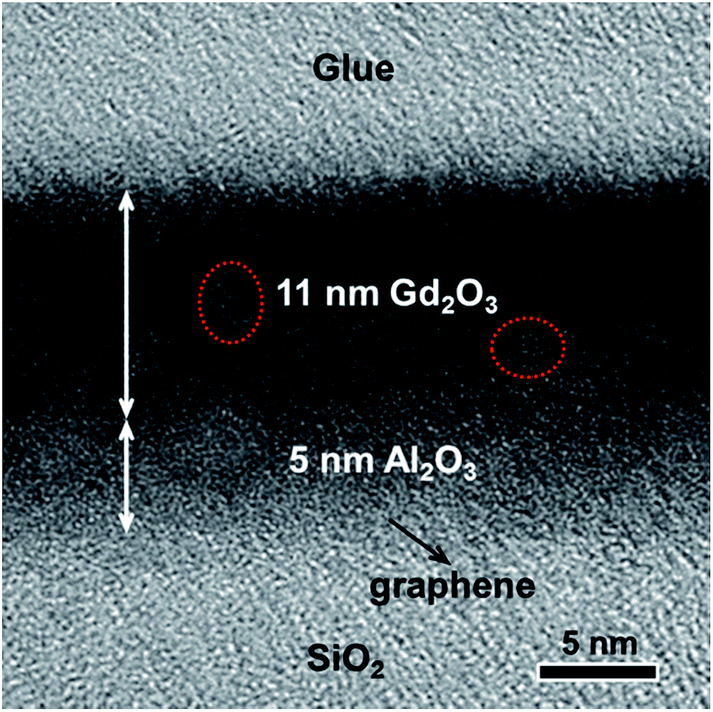 | ||
| Fig. 3 A HRTEM image of Al2O3–Gd2O3 double-films on graphene. Al2O3 deposited at 100 °C was 5 nm and Gd2O3 deposited at 200 °C was 11 nm. | ||
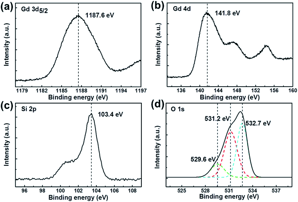
Fig. 4 demonstrates the results of XPS analysis to confirm all of elements present in the films. The binding energy was calibrated by centering the C 1s peak at 284.5 eV. The Gd 3d5/2 peak located at 1187.6 eV (Fig. 4a), separated by 1045.8 eV from the Gd 4d peak located at 141.8 eV (Fig. 4b), indicating the existence of Gd3+. In addition to Gd3+, the Si 2p peak located at 103.4 eV was also detected. The existence of Si in Gd2O3 films was probably generated from the oxidizing of by-products in eqn (1) during the ALD process.
| NH(SiMe)2 + 2H2O → SiO2 + NH5Me2 | (3) |
 | ||
| Fig. 4 XPS analysis of Al2O3–Gd2O3 double-films on graphene: Gd 3d5/2 (a), Gd 4d (b), Si 2p (c) and O 1s (d). | ||
As shown in eqn (3), the by-product, NH(SiMe)2, in eqn (1) could react with H2O, leading to the formation of SiO2 and this result could also be concluded from the analysis of O 1s peak illustrated in Fig. 4d. The O 1s peak was asymmetric and further deconvolution revealed three distinct components. The two stronger peak locating at 531.2 eV and 532.7 eV originated from Gd–O and Si–O bonds, respectively, and the weak peak at 529.6 eV associated with OH− hydroxyl groups due to the incomplete reaction of Gd[N(SiMe3)2]3/H2O. The atomic ratio of Si/Gd is about 0.96, indicating high concentration doping of Si in Gd2O3 film.
Spectroscopic ellipsometry was applied for the investigation of the optical constants (refractive index n, absorption coefficient α, and complex permittivity ε) of Al2O3–Gd2O3 double-films on graphene. The refractive index n and extinction coefficient k of Al2O3–Gd2O3 double-films were directly obtained from ellipsometry measurements. As shown in Fig. 5a, the refractive index n of Al2O3–Gd2O3 double-films on graphene presented increasing tendency with increase of wavelengths λ and it was approximately 3.2 in the visible region. The absorption coefficients α was calculated from the extinction coefficients k by the following formula: α = 4πk/λ. As illustrated in Fig. 5b, the absorption coefficients α of Al2O3–Gd2O3 double-films demonstrated increasing tendency with increase of the photon energy from 1.0 eV to 3.0 eV (1100 nm to 400 nm) and had an absorption peak in the range of 3.0 eV to 5.0 eV (400 nm to 250 nm). The complex permittivity ε (ε = εr − iεi) of Al2O3–Gd2O3 double-films on graphene could also be calculated from refractive index n and extinction coefficients k according to the following formulas: εr = n2 − k2 and εi = 2nk, where εr and εi are the real part and imaginary part of the complex permittivity, respectively (Fig. 5c). It was interesting to note that the real part of the complex permittivity εr was negative in the near ultraviolet region (from 220 nm to 400 nm), indicating that graphene/Al2O3–Gd2O3 might act as a meta material and applied to novel optical devices. The negative value of εr was due to the sudden enhancement of the extinction coefficients k in the near ultraviolet region as shown in the inset of Fig. 5c, and this enhancement was determined by the intrinsic properties of graphene/Al2O3–Gd2O3.
 | ||
| Fig. 5 Optical properties analysis of Al2O3–Gd2O3 double-films on graphene by spectroscopic ellipsometry: refractive index (a), absorption coefficient (b) and complex permittivity (c). | ||
C–V measurements were also employed to estimate the electrical properties of Al2O3–Gd2O3 double-films on graphene. A metal–oxide–graphene (MOG) structure was adopted in the electrical analysis shown in Fig. 6a. The areas of each electrode were 0.01 mm2 and the distance between two electrodes was 0.8 mm. The actual capacitance value was double of the measured one due to the series connection of two same capacitors. Fig. 6b showed the accurate model of MOG structure (left) and the series circuit model25 (middle) employed in the C–V measurements. The impedance of a MOG capacitor was given by
 | (4) |
 | (5) |
 | (6) |
 | ||
| Fig. 6 (a) The MOG structure. (b) The accurate model (left) and the series model (right) of MOG structure. (c), (d) C–V measurements of Gd2O3 films and Al2O3–Gd2O3 double-films performed at different frequencies: 200 kHz (curve a), 500 kHz (curve b), and modified by dual-frequency method (curve c), respectively. | ||
A dual-frequency method26 was introduced to correct for series resistance effects and to determine accurately the capacitance of Al2O3–Gd2O3 films. Measuring the capacitance at two different frequencies, substituting into (6) for each frequency, subtracting, and solving for C, one could obtain.
 | (7) |
The measured capacitance (Cm) was consisted of three components: the oxide capacitance (Cox), the quantum capacitance of graphene (Cq) and the capacitance induced by interface states (Cit), as shown in Fig. 6b (right). C–V measurements of Gd2O3 films and Al2O3–Gd2O3 double-films were both implemented at two frequencies (200 kHz and 500 kHz) and modified by eqn (7) as shown in Fig. 6c and d, respectively. All the C–V measurements showed the expected broad V-shape induced by the quantum capacitance (Cq) of graphene,27,28 indicating Cit did not play a major role in the measured capacitance (Cm), or the V-shape curve would not be detected. In addition, Cq was in parallel to Cit, while both of them were in series to the oxide capacitance (Cox), and Cox was approximately an order of magnitude lower than Cq at the bias away from the Dirac point of graphene. Thus, the measured capacitance at ±2 V was close to Cox. The capacitances of Gd2O3 films and Al2O3–Gd2O3 double-films were 0.64 μF cm−2 and 0.58 μF cm−2, while the relative permittivities were 15 and 11, respectively. The permittivity reduction of Al2O3–Gd2O3 double-films was due to the relatively small permittivity of Al2O3 (7–9). However, the introduction of an Al2O3 seed-like layer was beneficial to both the surface morphology and compactness of subsequently deposited Gd2O3 films.
Conclusions
In summary, we have directly deposited Gd2O3 films and Al2O3–Gd2O3 double-films onto pristine graphene by ALD. No additional defects are introduced into graphene after high-κ films deposition. The introduction of an Al2O3 seed-like layer benefits both the surface morphology and compactness of subsequently deposited Gd2O3 films. The surface RMS of Al2O3–Gd2O3 double-films is down to 0.8 nm and the relative permittivity is around 11, which indicate high quality of high-κ films. This technique provides scientific guidance in fabricating novel graphene-based electronic devices.Acknowledgements
This work is funded by the National Natural Science Foundation of China (Grant no. 11175229).We would like to thank Prof. Zengfeng Di, Dr Gang Wang, Dr Xiaohu Zheng and Dr Haoran Zhang for their generous help.Notes and references
- K. S. Novoselov, A. K. Geim, S. V. Morozov, D. Jiang, Y. Zhang, S. V. Dobonos, I. V. Grigorieval and A. A. Firsov, Science, 2004, 306, 666–669 CrossRef CAS PubMed.
- A. A. Balandin, S. Ghosh, W. Bao, I. Calizo, D. Teweldebrhan, F. Miao and C. N. Lau, Nano Lett., 2008, 8, 902–907 CrossRef CAS PubMed.
- M. D. Stoller, S. Park, Y. Zhu, J. An and R. S. Ruoff, Nano Lett., 2008, 8, 3498–3502 CrossRef CAS PubMed.
- C. Lee, X. Wei, J. W. Kysar and J. Hone, Science, 2008, 321, 385–388 CrossRef CAS PubMed.
- B. H. Lee, J. Oh, H. H. Tseng, R. Jammy and H. Huff, Mater. Today, 2006, 9, 32–37 CrossRef CAS.
- L. Wang, J. J. Travis, A. S. Cavanagh, X. Liu, S. P. Koenig, P. Y. Huang, S. M. George and J. S. Bunch, Nano Lett., 2012, 12, 3706–3710 CrossRef CAS PubMed.
- W. C. Shin, T. Y. Kim, O. Sul and B. J. Cho, Appl. Phys. Lett., 2012, 101, 033507 CrossRef PubMed.
- J. C. G. Buenzil and C. Piguet, Chem. Soc. Rev., 2005, 34, 1048–1077 RSC.
- J. Kido and Y. Okamoto, Chem. Rev., 2002, 102, 2357–2368 CrossRef CAS PubMed.
- J. Robertson, Eur. Phys. J.: Appl. Phys., 2004, 28, 2357 CrossRef.
- W. H. Chang, C. H. Lee, Y. C. Chang, P. Chang, M. L. Huang, Y. J. Lee, C. Hsu, J. M. Hong, C. C. Tsai, J. R. Kwo and M. Hong, Adv. Mater., 2009, 21, 4970–4974 CrossRef CAS.
- A. P. Milanov, K. Xu, A. Laha, E. Bugiel, R. Ranjith, D. Schwendt, H. J. Osten, H. Parala, R. A. Fischer and A. Devi, J. Am. Chem. Soc., 2010, 132, 36–37 CrossRef CAS PubMed.
- K. Xu, R. Ranjith, A. Laha, H. Parala, A. P. Milanov, R. A. Fischer, E. Bugiel, J. Feydt, S. Irsen, T. Toader, C. Bock, D. Rogalla, H. Osten, U. Kunze and A. Devi, Chem. Mater., 2012, 24, 651–658 CrossRef CAS.
- M. J. Hollander, M. LaBella, Z. R. Hughes, M. Zhu, K. A. Trumbull, R. Cavalero, D. W. Snyder, X. J. Wang, E. Hwang, S. Datta and J. A. Robinson, Nano Lett., 2011, 11, 3601–3607 CrossRef CAS PubMed.
- B. Lee, G. Mordi, M. J. Kim, Y. J. Chabal, E. M. Vogel, R. M. Wallace, K. J. Cho, L. Colombo and J. Kim, Appl. Phys. Lett., 2010, 97, 043107 CrossRef PubMed.
- Y. Xuan, Y. Q. Wu, T. Shen, M. Qi, M. A. Capano, J. A. Cooper and P. D. Ye, Appl. Phys. Lett., 2008, 92, 013101 CrossRef PubMed.
- D. B. Farmer, H. Y. Chiu, Y. M. Lin, K. A. Jenkins, F. N. Xia and P. Avouris, Nano Lett., 2009, 9, 4474–4478 CrossRef CAS PubMed.
- Y. M. Lin, K. A. Jenkins, A. V. Garcia, J. P. Small, D. B. Farmer and P. Avouris, Nano Lett., 2009, 9, 422–426 CrossRef CAS PubMed.
- L. Zheng, X. Cheng, D. Cao, G. Wang, Z. Wang, D. Xu, C. Xia, L. Shen, Y. Yu and D. Shen, ACS Appl. Mater. Interfaces, 2014, 6, 7014–7019 CAS.
- T. M. G. Mohiuddin, A. Lombardo, R. R. Nair, A. Bonetti, G. Savini, R. Jalil, N. Bonini, D. M. Basko, C. Galiotis, N. Marzari, K. S. Novoselov, A. K. Geim and A. C. Ferrari, Phys. Rev. B: Condens. Matter Mater. Phys., 2009, 79, 205433 CrossRef.
- J. A. Robinson, M. LaBella, K. A. Trumbull, X. Weng, R. Cavelero, T. Daniels, Z. Hughes, M. Hollander, M. Fanton and D. Snyder, ACS Nano, 2010, 4, 2667–2672 CrossRef CAS PubMed.
- S. Pisana, M. Lazzeri, C. Casiraghi1, K. S. Novoselov, A. K. Geim, A. C. Ferrari and M. Maur, Nat. Mater., 2007, 6, 198–201 CrossRef CAS PubMed.
- A. Das, S. Pisana, B. Chakraborty, S. Piscanec, S. K. Saha, U. V. Waghmare, K. S. Novoselov, H. R. Krishnamurthy, A. K. Geim, A. C. Ferrari and A. K. Sood, Nat. Nanotechnol., 2008, 3, 210–215 CrossRef CAS PubMed.
- H. Xu, Y. B. Chen, J. Zhang and H. L. Zhang, Small, 2012, 8, 2833–2840 CrossRef CAS PubMed.
- K. J. Yang and C. Hu, IEEE Trans. Electron Devices, 1999, 46, 1500–1501 CrossRef CAS.
- Z. Luo and T. P. Ma, IEEE Electron Device Lett., 2004, 25, 655–657 CrossRef.
- T. Fang, A. Konar, H. Xing and D. Jena, Appl. Phys. Lett., 2007, 91, 092109 CrossRef PubMed.
- J. Xia, F. Chen, J. Li and N. Tao, Nat. Nanotechnol., 2009, 4, 505–509 CrossRef CAS PubMed.
| This journal is © The Royal Society of Chemistry 2014 |