The improvement of thin film barrier performances of organic–inorganic hybrid nanolaminates employing a low-temperature MLD/ALD method

Wang Xiaoa, Duan Yu*a, Sun Feng Bob, Yang Yong Qianga, Yang Dana, Chen Pinga, Duan Ya Huia and Zhao Yia
aState Key Laboratory on Integrated Optoelectronics, College of electronic science and engineering, Jilin University, Changchun 130012, Jilin, China. E-mail: duanyu@jlu.edu.cn; Fax: +86 0431-85168270; Tel: +86 0431-85168243-8217 Tel: +86 13756531922
bCollege of Science, Changchun University of Science and Technology, Jilin 130022, China

Received 4th July 2014 , Accepted 5th September 2014

First published on 5th September 2014


Abstract

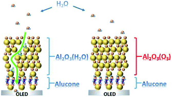
The investigations reported in this study were carried out to determine the feasibility and properties of alucone/Al2O3 hybrid nanolaminate films for thin film encapsulation (TFE) at low temperature, using an integrated molecular layer deposition (MLD) and atomic layer deposition (ALD) process. The combination of alucone (MLD) and Al2O3 (ALD), with O3 serving as the oxidant in place of conventional H2O, has been evaluated experimentally. In our studies, O3-based encapsulation layers were observed to be smoother, displaying an average roughness of 0.342 ± 0.016 nm with three laminate layers. However, H2O-based laminates showed a much higher roughness of 0.843 ± 0.024 nm under identical conditions. Estimates of water vapor transmission rate (WVTR) yielded significantly better results for O3-based laminates, with values decreasing linearly from 3.22 × 10⁻³ g m−2 per day to 2.37 × 10⁻⁵ g m−2 per day as the number of laminate layers increased from one to three, while a gentle decline trend from 1.83 × 10⁻³ g m−2 per day to 5.92 × 10⁻⁴ g m−2 per day was obtained for the H2O-based laminate. This indicates that the hybrid nanolaminates exhibited improved water barrier properties when O3 was used as the oxidant instead of H2O. In particular, the O3-based films did not decrease the performance of organic light-emitting diodes (OLEDs). In fact, the lifetime of OLEDs with O3-based encapsulation was approximately two-fold longer than the H2O-based encapsulation. Thus, we believe that the alucone/Al2O3 hybrid encapsulation film, in which O3 serves as the oxidant, is a promising candidate for use in future OLED applications.


1. Introduction

Organic light-emitting diodes (OLEDs) represent a relatively recent technological innovation offering many important advantages, including low power consumption, high brightness, low cost, fast response, and thin structure.1–3 Unfortunately, most organic active materials and metal electrodes in OLEDs are easily oxidized when exposed to water vapor and oxygen in the air, which produces dark spots and edge shrinkage over the light-emitting areas. OLED degradation due to air-permeation can therefore become a major drawback, which limits their practical utility.4,5

These limitations are being overcome with the advent of new OLED encapsulation technologies, and significant research is now focused on the development of thin film encapsulation (TFE) as one of the most effective ways to solve OLED degradation due to air-permeation.6–13 Among established TFE technologies, the atomic layer deposition (ALD) technique has been widely reported.8–13 This novel thin film deposition technique is able to produce accurately controlled conformal inorganic film.

Compared to traditional inorganic encapsulation structure deposited by ALD, alternating inorganic and organic multibarrier stacks (nanolaminates) have also been proposed for ultra-low gas diffusion barrier film applications.14–16 Nanolaminate structures exhibit improved barrier performance, for two reasons: (i) the organic layer in nanolaminates serves as a type of resistive interlayer that appears to lengthen the diffusion path for water permeation, and (ii) nanolaminates exhibit properties that inhibit the propagation of defects through the multilayer structure. Both of these characteristics are beneficial as they improve the associated water vapor transmission rate (WVTR).11,12

In fact, there is another technique to prepare thin films, namely, molecular layer deposition (MLD).17,18 MLD was initially developed for growing organic polymers such as polyamides and polyimides. However, various organic materials can also be deposited by MLD with different reactants.17,18 Therefore, we selected ALD and MLD for inorganic/organic nanolaminates to avoid pollutants being transferred (Table 1).

Table 1 Summary of surface characteristics and barrier properties after deposition by ALD/MLD, including film thickness, normalized growth rate, RMS by AFM, and WVTR
Film code Total film thickness (nm) Normalized growth rate (Å per cycle) RMS (nm) WVTR (g m−2 per day)
(a) 25.621 ± 0.721 1.25 0.480 ± 0.013 1.83 × 10⁻³
(b) 53.181 ± 0.532 1.12 0.563 ± 0.039 1.45 × 10⁻³
(c) 79.100 ± 0.721 1.01 0.843 ± 0.024 5.92 × 10⁻⁴
(d) 26.471 ± 0.069 1.29 0.251 ± 0.015 3.22 × 10⁻³
(e) 55.644 ± 0.143 1.16 0.275 ± 0.027 4.24 × 10⁻⁴
(f) 79.247 ± 0.542 1.01 0.342 ± 0.016 2.37 × 10⁻⁵


Moreover, organic precursors of MLD techniques have been found to be thermally sensitive to decomposition at higher temperatures. Consequently, it has become clear that ALD/MLD processes must operate at low temperatures if they are to facilitate practical methods of OLED encapsulation.9,10 Unfortunately, with low temperature MLD/ALD methods, the conventional use of H2O as an encapsulation oxidant may cause residual condensation, which can generate undesirable subsidiary reactions leading to significant pin-hole and other low density defects inside the encapsulation film.19 Therefore, the replacement of O3 with H2O has been considered to avoid these side effects, thus improving the barrier performance eventually.

In this study, we investigated the feasibility and properties of alucone/Al2O3 hybrid nanolaminate films for TFE using an MLD/ALD method at a very low temperature (<100 °C), with O3 serving as the oxidant instead of H2O.20,21 Herein, alucone refers to a type of poly(aluminum ethylene glycol) polymer, whose chemical composition is (–Al–O–C2H4–O–)n.22 The structures of the multilayer hybrid nanolaminate grown using H2O and O3 as the oxidants were thoroughly investigated by atomic force microscopy (AFM), scanning electron microscopy (SEM), and spectroscopic ellipsometer studies. The compatibility of the alucone/Al2O3 for OLED was studied by WVTR, I–V–L, and lifetime measurements under ambient conditions of 20 °C and 60% relative humidity (RH). The variation in the multilayer alucone/Al2O3 structure afforded tunable barrier properties.

2. Experiments

In order to compare film properties and barrier performance, we fabricated two groups of nanolaminates based on H2O and O3 oxidants, respectively. Films (a)–(c) were made using H2O as the oxidant, while films (d)–(f) used O3. The detailed composition of the films is shown in Fig. 2. Based on previous research,23 the ratio of alucone to Al2O3 of 1[thin space (1/6-em)]:[thin space (1/6-em)]5 or less for the alucone/Al2O3 encapsulation layer would result in low permeation from water vapor and oxygen. Both Al2O3 and alucone film were deposited using a LabNano 9100 ALD system (Ensure Nanotech Inc.) at 80 °C, and the temperature of all pipes was set to 120 °C. The pressure in the reaction chamber was 3 × 10⁻² Pa.

For growth of the Al2O3 inorganic layer, Al(CH3)3 (trimethylaluminum or TMA), Sigma Aldrich, deionized water or O3 were prepared as precursors of Al and O, separately. O3 was produced by an ozone generator in our experiments where a mixture of oxygen (400 sccm, 99.999%) and catalytic nitrogen (5 sccm) was used to generate 3.5 wt% O3, with a concentration of around 50 mg L−1. During the growing process, high-purity N2 (flow rate, 20 sccm) was used as carrier gas for these precursors. A single Al2O3 (H2O-based) cycle consisted of the following sequence: 0.02 s TMA dose, 30 s nitrogen purge, 0.02 s H2O dose, and 30 s nitrogen purge.24 However, when O3 was used as the oxidant, the pulsing time was extended to 0.1 s and purge time was reduced to 10 s. This sequence was repeated for the desired number of ALD cycles.

For the growth of the alucone organic layer, TMA and HO–(CH2)2–OH (ethylene glycol (EG), Sigma Aldrich) were chosen as reactants under identical conditions. Prior to the deposition reaction, EG was preheated to 95 °C to increase its vapor pressure.25 Similar to the ALD procedure, the following timing sequence was established to fabricate alucone: 0.02 s TMA dose, 30 s nitrogen purge, 0.07 s EG dose, and 120 s nitrogen purge. We optimized Al2O3 (ALD) and alucone (MLD) films to maintain the growth step to between 1.00–1.20 Å per cycle.

Fig. 1 shows the schematic diagram of alucone (MLD) and Al2O3 (ALD) growth based on H2O.22 For alucone (MLD), a hydroxylated surface is exposed to TMA, and CH4 is released as a by-product. After eliminating CH4 and unreacted reactants by inert gas, the resulting surface is then exposed to EG, and CH4 is released again as a by-product. Besides, the surface is left covered with hydroxyl groups for the next cycle. This is the same procedure for Al2O3 (ALD) except for the substitution of H2O with EG.


image file: c4ra06638c-f1.tif
Fig. 1 Schematic outline of the procedure to fabricate Al2O3 and alucone thin films using atomic layer deposition and molecular layer deposition respectively.

image file: c4ra06638c-f2.tif
Fig. 2 A schematic diagram of prepared TFE structures: films (a) and (d) #1alucone (4 nm)/Al2O3 (20 nm) films (b) and (e) #2[alucone (4 nm)/Al2O3 (20 nm)] × 2 films (c) and (f) #3[alucone (4 nm)/Al2O3 (20 nm)] × 3.

WVTR measurements were carried out to test the barrier performance of the encapsulation films using the calcium (Ca) corrosion test method, in which metal calcium reacts easily with the infiltrated water vapor. The amount of oxidized Ca was then utilized to calculate the amount of water vapor permeated through the encapsulation film. The calculated WVTR was determined with the following formula:14

 
image file: c4ra06638c-t1.tif(1)
where n is mole ratio of the chemical reaction (n = 2); δCa is Ca resistivity (3.4 × 10⁻⁶ Ω m); ρCa is Ca density (1.55 g cm−3); (1/R) was the conductance measured from our samples during the tests; M(H2O) and M(Ca) are the molar masses of water vapor and Ca, respectively, and Ca_Area/Window_Area represents the effective testing area to mask window area ratio (n = 1).

In our experiments, all electrical measurements were made using electrodes connected by a SMU to an Agilent 2920 source meter. The root-mean-square (RMS) roughness and other surface features of the films were measured with a Veeco AFM. SEM was conducted with a field-emission SEM (JSM-6700F, JEOL), operating at an accelerating voltage of 10 kV to give a clear picture on the cross-section. All the samples were coated with a thin layer of gold (5 nm) prior to analysis. The thickness and refractive index of the deposited thin films were measured using a J.A. Woolam variable-angle spectroscopic ellipsometer.

3. Results and discussion

First, all the hybrid films were deposited on clean Si substrates at 80 °C. Their surface morphological characteristics were observed through a scanned area of 0.5 × 0.5 μm2 by AFM. While H2O-based films were relatively rough, as clearly shown in Fig. 3(a)–(c), the O3-based films showed a smoother, more homogeneous structure in Fig. 3(d)–(f). The RMS variation of the H2O-based films rose rapidly from 0.480 ± 0.013 nm for film (a) to 0.843 ± 0.024 nm for film (c). This increase was attributed to the likelihood that H2O might condense due to low deposition temperature, which would create difficulty in removing residual condensation from the chamber with the purge gas. As a result, impurity particles caused by a CVD-type reaction between residual H2O and the following precursor would appear to be responsible for the resulting higher RMS. However, for films grown with O3, no distinct changes in roughness were seen with increasing number of laminate, as shown in Fig. 3(d)–(f). The measured RMS values in this case were 0.251 ± 0.015 nm for film (d), while for film (f), the value increased slightly to 0.342 ± 0.016 nm. This phenomenon implying the likelihood of an atomically smooth surface (for O3-based films) characterized by a 2D layer-by-layer growth mode.
image file: c4ra06638c-f3.tif
Fig. 3 Atomic force microscope (AFM) images on clean Si substrate: films (a)–(c) based on H2O; films (d)–(f) based on O3.

In the TMA + H2O process,26 the water and methane by-products cannot be efficiently purged out under low temperature conditions, resulting in an incomplete chain-reaction.17 Furthermore, EG has strong hydrophilic characteristics because of the OH bond in the molecular structure.27,28 The dipole–dipole forces among the OH bonds between EG and water bring them together, easily. This enables the TMA chemical groups to react with the H2O continually during deposition.29 These “CVD” type reactions lead to a loss of active surface sites on the surface and an increase in the occurrence of defects, which has been identified as the most significant drawback issue, i.e., the limited continuous pinhole-free nature of Al2O3 films, when using low temperature ALD.10

To further investigate the internal growth states of hybrid films deposited by H2O or O3 as oxidants under low temperature conditions, cross-sectional information for the alucone/Al2O3 films was studied through SEM. We chose film (c) and film (f) to study this aspect. Both of the films were deposited directly onto clean Si substrates at 80 °C. As shown in Fig. 4(1), when H2O was used as the oxidant, no obvious interface between alucone (MLD) and Al2O3 (ALD) was observed. Therefore, we believed that the alucone layer might not grow properly in this case because the residual H2O adsorption at low temperature and the resulting effects on TMA could well degrade the reaction between TMA and EG. As a result, continuous growth may be interrupted and impurities might be accumulated.30 However, we could clearly see some strips of shallow parts inside the laminate structure of O3-based film (Fig. 4(2)). Here, alucone was completely formed since adequate reaction between EG and TMA had occurred. Furthermore, we believed that O3 has higher chemical reactivity to TMA and generates more active groups on the surface, which could facilitate the reaction.


image file: c4ra06638c-f4.tif
Fig. 4 The cross-sectional image from SEM for the 80 nm-thick nanolaminate films (c) and (f) deposited directly on clean Si substrates at 80 °C.

In order to verify the barrier properties of the hybrid laminate films deposited by H2O or O3 as oxidants under different reaction cycles, WVTR measurements were carried out using the calcium (Ca) corrosion test method mentioned earlier. This method takes advantage of calcium degradation by monitoring its resistive change in Ohmic behavior.24 A 200 nm calcium layer with an area of 1 × 1 cm2 was deposited via thermal evaporation on clean glass with 100 nm patterned aluminum as electrodes. Fig. 5(1) and (2) compared the variation trend of normalized conductance as a function of time at 20 °C and 60% RH, between hybrid films based on H2O and O3, respectively. Samples with O3-based TFE revealed a much more stable trend versus operating time than samples with H2O-based TFE, except for one laminate layer: both of which exhibited a rapid decline tendency. WVTR values were calculated for different numbers of laminate layers as shown in the inset of Fig. 5(1) and (2). It is obvious that the WVTR of alucone/Al2O3 (O3-based) TFE decreased sharply with the increasing laminate number from 3.22 × 10⁻³ g m−2 per day (one laminate pair) to 2.37 × 10⁻⁵ g m−2 per day (three laminate pairs). The H2O-based measurements exhibited a rather flat downtrend from 1.83 × 10⁻³ g m−2 per day (one laminate pair) to 5.92 × 10⁻⁴ g m−2 per day (three laminate pairs). Some previous studies14 obtained 3.73 × 10⁻² g m−2 per day for 50 nm Al2O3 single layer and 1.14 g m−2 per day for 50 nm alucone single layer. However, the values were still higher than 1.83 × 10⁻³ g m−2 per day the highest value obtained for 25 nm alucone/Al2O3 based on H2O in this study. Thus, this alucone/Al2O3 hybrid encapsulation structure may be superior in preventing water vapor permeation. According to previous research,12 alucone can prolong the permeation path and suppress permeation speed as it reacts readily with H2O,24 thus contributing to better barrier performance. As for H2O-based hybrid film, its performance is mostly affected perhaps due to its intrinsic properties during the deposition process. The emergence of impurities or voids may create resistive paths for water vapor and oxygen, which could account for the unsatisfying barrier performance. Fig. 6 shows the optical images of the Ca corrosion test device after exposed to ambient conditions of 20 °C and 60% RH for 140 h. The transparent area is Ca(OH)2. Clearly, O3-based film was superior to H2O-based film in preventing water vapor and oxygen diffusion under identical conditions.


image file: c4ra06638c-f5.tif
Fig. 5 Normalized change in electrical conductance of Ca corrosion tests with TFE (a)–(f) as a function of time at 20 °C and 60% RH. (1) H2O-based, (2) O3-based, the insert shows the calculated water vapor transmission rate (WVTR) changes versus number of laminates.

image file: c4ra06638c-f6.tif
Fig. 6 Optical images of the Ca corrosion test device at ambient condition of 20 °C and 60% RH, encapsulated with films (a)–(f) after 140 h test.

During the next stage of our experiments, we evaluated the effects of these hybrid encapsulation films on OLED devices. I–V–L characteristics were examined to study the electrical behavior of the OLED devices before and after coating with the encapsulation films. The structure of the OLED samples was as follows:

Indium Tin Oxide (ITO) glass as anode.

5 nm thick MoO3 as a modified layer.

30 nm thick 4,4′,4′′-tris(N-3(3-methylphenyl)-N-phenylamino)triphenylamine (m-MTDATA) as a hole injection layer.

20 nm thick N,N′-biphenyl-N,N′bis(1-naphenyl)-[1,1′-biphenyl]-4,4′-diamine(NPB) as a hole transport layer.

20 nm thick tris(8-hydroxyquinoline)aluminum (Alq3) as a light-emitting layer.

30 nm Alq3 as an electron transport layer.

1 nm thick LiF as a buffer layer.

100 nm thick Al as cathode.

The active area of the samples was 3 × 3 mm2. The OLED samples were deposited using a thermal evaporation equipment at 5 × 10⁻⁴ Pa without breaking the vacuum and then transferred to a glove box under pure nitrogen immediately for the encapsulation with ALD and MLD techniques. The electrical and emission characteristics of these samples were measured using an Agilent 2920 source meter, a Minolta luminance meter LS-110, and a PR650 spectrometer in air at room temperature. The I–V–L characteristics of the OLED samples are shown in Fig. 7. Only slight differences in I–V behavior were observed for the devices with or without the encapsulation structure. This result indicates that the deposition temperature of 80 °C did not deteriorate the devices. Besides, as a highly reactive oxidant, O3 hardly caused any damage to the active layer or metal cathode. The reaction for Al2O3 (ALD) in the deposition chamber occurred above the alucone (MLD) layer. As Al2O3 kept growing on the top of the OLEDs, the effect of this exposure became very weak in each ALD cycle.


image file: c4ra06638c-f7.tif
Fig. 7 Luminance–voltage and current density–voltage vs. operational voltage characteristics for bare OLEDs, OLEDs encapsulated with films (a)–(f) (1) films based on H2O (2) films based on O3.

The luminance decay versus operating time for one laminate layer structure was also observed under ambient conditions, and the results are shown in Fig. 8. All the measurements were carried out non-stop at a DC voltage, and the OLED devices were burned for 100 s to minimize the increase in brightness immediately after turn-on. Lifetime is expressed as follows:

 
image file: c4ra06638c-t2.tif(2)
where L0 is the initial luminance, τ and β are fitting parameters.31 We define the lifetime as the time required to reach L/L0 = 0.5, which is the time that elapses before the instantaneous luminance of the OLEDs reaches 50% of its initial value. In this study, the lifetimes were measured from nearly L0 = 860 cd m−2 as the initial luminance. In Fig. 8, the bare device in controlled ambient air degraded very fast, indicating that the degradation caused by O2 and H2O permeated the devices. The OLEDs with O3-based hybrid TFE had a lifetime of 50 h, which was approximately two-fold longer than the H2O-based hybrid TFE. Clearly, the lifetime of the O3-based TFE device was prolonged considerably, compared to the device with or without H2O-based encapsulation film under identical conditions. In fact, even in nominally O2 and H2O-free environment, remarkable degradation could still be observed, consistent with those reported elsewhere for NPB/Alq3 based OLEDs whose Alq3 cations are unstable fluorescence quenchers.32,33 This result confirmed that the O3-based hybrid encapsulation layer exhibited superior barrier performance than the H2O-based layer when used in OLED devices.


image file: c4ra06638c-f8.tif
Fig. 8 Normalized experimental luminance decay as a function of continuous operating time for OLEDs encapsulated with film (a) or (d) measured at ambient conditions of 20 °C, 60% RH.

4. Conclusion

In summary, we have demonstrated that the alucone/Al2O3 nanolaminate encapsulation layer, which utilizes O3 instead of H2O as oxidant at 80 °C, exhibits better barrier performance. Through the observation of AFM and SEM, more uniform and flat surface characteristics were also detected from the O3-based film. The RMS values for these films were no more than 0.350 nm, while the values for H2O-based films rose quickly from 0.480 ± 0.013 nm to 0.843 ± 0.024 nm. O3-based hybrid encapsulation layers exhibited an accentuated declining trend in WVTR from 3.22 × 10⁻³ g m−2 per day to 2.37 × 10⁻⁵ g m−2 per day as the laminate increased from one to three at 20 °C, 60% RH. For H2O-based film, a gentle drop-off from 1.83 × 10⁻³ g m−2 per day to 5.92 × 10⁻⁴ g m−2 per day was observed under identical conditions. From I–V–L measurements, we found that O3-based encapsulation films did not destroy the performance of OLEDs. Indeed, the lifetime of OLEDs with O3-based encapsulation was approximately two-fold longer than the H2O-based encapsulation. As a result of our investigations, we believe that alucone/Al2O3 hybrid encapsulation film, where O3 serves as the oxidant, is a promising candidate for use in future TFE devices. Subsequent work will expand the capabilities of the MLD/ALD method to deposit flexible barrier layers to promote the practical applications of OLED.

Acknowledgements

This study was supported by the Program of International Science and Technology Cooperation (2014DFG12390), National High Technology Research and Development Program of China (Grant no. 2011AA03A110), Ministry of Science and Technology of China (Grant no. 2010CB327701, 2013CB834802), the National Natural Science Foundation of China (Grant nos 61275024, 61274002, 61275033, 61377206 and 41001302), Scientific and Technological Developing Scheme of Jilin Province (Grant no. 20140101204JC, 20140520071JH), Scientific and Technological Developing Scheme of Changchun (Grant no. 13GH02), and the Opened Fund of the State Key Laboratory on Integrated Optoelectronics no. IOSKL2012KF01.

References

  1. K. Zhang, C. M. Zhong, S. J. Liu, A. H. Liang, S. Dong and F. Huang, J. Mater. Chem. C, 2014, 2, 3270–3277 RSC.
  2. Q. Li, L. S. Cui, C. Zhong, Z. Q. Jiang and L. S. Liao, Org. Lett., 2014, 16, 1622–1625 CrossRef CAS PubMed.
  3. S. J. Su, C. Cai, J. Takamatsu and J. Kido, Org. Electron., 2012, 13, 1937–1947 CrossRef CAS PubMed.
  4. S. Park, W. M. Yun, L. H. Kim, S. Park, S. H. Kim and C. E. Park, Org. Electron, 2013, 14, 3385 CrossRef CAS PubMed.
  5. D. Yang, Y. Q. Yang, Y. Duan, P. Chen, C. L. Zang, Y. Xie, D. M. Liu, X. Wang, Y. H. Duan, F. B. Sun, Q. Gao and K. W. Xue, ECS Solid State Lett., 2013, 2, 31–33 CrossRef PubMed.
  6. S. H. K. Park, J. Oh, C. S. Hwang, J. I. Lee, Y. S. Yang, H. Y. Chu and K. Y. Kang, ETRI J., 2005, 27, 545–550 CrossRef.
  7. H. K. Kim, M. S. Kim, J. W. Kang, J. J. Kim and M. S. Yi, Appl. Phys. Lett., 2007, 90, 013502 CrossRef PubMed.
  8. S. J. Yun, Y. W. Ko and J. W. Lim, Appl. Phys. Lett., 2004, 85, 4896–4898 CrossRef CAS PubMed.
  9. S. M. George, Chem. Rev., 2010, 110, 111–131 CrossRef CAS PubMed.
  10. M. D. Groner, F. H. Fabreguette, J. W. Elam and S. M. George, Chem. Mater., 2004, 16, 639–645 CrossRef CAS.
  11. J. D. Affinito, M. E. Gross, C. A. Coronado, G. L. Graff, I. N. Greenwell and P. M. Martin, Thin Solid Films, 1996, 290, 63–67 CrossRef.
  12. J. Greener, K. C. Ng, K. M. Vaeth and T. M. Smith, J. Appl. Polym. Sci., 2007, 106, 3534–3542 CrossRef CAS PubMed.
  13. A. P. Ghosh, L. J. Gerenser, C. M. Jarman and J. E. Fornalik, Appl. Phys. Lett., 2005, 86, 223503 CrossRef PubMed.
  14. M. Park, S. Oh, H. Kim, D. Jung, D. Choi and J. S. Park, Thin Solid Films, 2013, 546, 153–156 CrossRef CAS PubMed.
  15. K. H. Jung, J. Y. Bae, S. J. Park, S. Yoo and B. S. Bae, J. Mater. Chem., 2011, 21, 1977–1983 RSC.
  16. Y. C. Han, E. Kim, W. Kim, H. G. Im, B. S. Bae and K. C. Choi, Org. Electron., 2013, 14, 1435–1440 CrossRef CAS PubMed.
  17. T. Yoshimura, S. Tatsuura and W. Sotoyama, Appl. Phys. Lett., 1991, 59, 482–484 CrossRef CAS PubMed.
  18. P. Sundberg, A. Sood, X. Liu and M. Karppinen, Dalton Trans., 2013, 42, 15043–15052 RSC.
  19. Y. Q. Yang, Y. Duan, P. Chen, F. B. Sun, Y. H. Duan, X. Wang and D. Yang, J. Phys. Chem. C, 2013, 117, 20308–20312 CAS.
  20. S. Sarkar, J. H. Culp and J. T. Whyland, Org. Electron., 2010, 11, 1896–1900 CrossRef CAS PubMed.
  21. Y. Q. Yang, Y. Duan, Y. H. Duan, X. Wang, P. Chen, D. Yang, F. B. Sun and K. W. Xue, Organ. Electron., 2014, 15, 1120–1125 CrossRef CAS PubMed.
  22. A. A. Dameron, D. Seghete, B. B. Burton, S. D. Davidson, A. S. Cavanagh, J. A. Bertrand and S. M. George, Chem. Mater., 2008, 20, 3315–3326 CrossRef CAS.
  23. S. H. Jen, B. H. Lee, S. M. George, R. S. McLean and P. F. Carcia, Appl. Phys. Lett., 2012, 101, 234103 CrossRef PubMed.
  24. Y. Park, K. S. Han, B. H. Lee, S. Cho, K. H. Lee and S. Im, Org. Electron., 2011, 12, 348–352 CrossRef CAS PubMed.
  25. X. Liang, D. M. King and P. Li, et al., AIChE J., 2009, 55, 1030–1039 CrossRef CAS PubMed.
  26. B. H. Lee, B. Yoon, V. R. Anderson and S. M. George, J. Phys. Chem. C, 2012, 116, 3250–3257 CAS.
  27. Y. D. Shen, Y. W. Li, J. Z. Zhang, X. Zhu, Z. G. Hu and J. H. Chu, Optoelectron. Adv. Mater., 2012, 6, 618–622 CAS.
  28. Y. Koga, J. Solution Chem., 2003, 32, 803–818 CrossRef CAS.
  29. S. M. George, B. Yoon and A. A. Dameron, Acc. Chem. Res., 2009, 42, 498–508 CrossRef CAS PubMed.
  30. M. J. Kao, D. C. Tien, C. S. Jwo and T. T. Tsung, J. Phys.: Conf. Ser., 2005, 13, 442–445 CrossRef CAS.
  31. C. Fery, B. Racine, D. Vaufrey, H. Doyeux and S. Cinà, Appl. Phys. Lett., 2005, 87, 213502 CrossRef PubMed.
  32. Z. D. Popovic, H. Aziz, N. X. Hu, A. M. Hor and G. Xu, Synth. Met., 2000, 111, 229–232 CrossRef.
  33. H. Aziz, Z. D. Popovic, N. X. Hu, A. M. Hor and G. Xu, Science, 1999, 283, 1900–1902 CrossRef CAS.

This journal is © The Royal Society of Chemistry 2014
Click here to see how this site uses Cookies. View our privacy policy here.