DOI:
10.1039/C4RA06531J
(Paper)
RSC Adv., 2014,
4, 44547-44554
Highly selective and sensitive CdS thin film sensors for detection of NO2 gas
Received
2nd July 2014
, Accepted 10th September 2014
First published on 12th September 2014
Abstract
We demonstrate the preparation of cadmium sulfide (CdS) thin films via a facile chemical bath deposition method. The CdS films have been characterized by various techniques, such as, X-ray diffraction (XRD), energy dispersive X-ray (EDAX), scanning electron microscopy (SEM) and transmission electron microscopy (TEM). Gas sensing performance of CdS thin films was tested at room temperature (38 °C) for oxidizing (NO2, Cl2) and reducing gases (H2S, NH3, C2H5OH, CH3OH). CdS films were found to be highly selective and sensitive to NO2 with a maximum response of 61% at 200 ppm with a fast response time of 50 s and 81% stability. Furthermore, the sensor is able to detect up to low (5 ppm) concentration of NO2 gas with a reasonable response (5%). The plausible mechanism(s) of NO2 sensing has been discussed.
1. Introduction
In recent years, a lot of studies on various materials as gas sensors have been reported. Gas sensors are very important in environmental monitoring, chemical control and home safety. The development of efficient devices for monitoring hazardous and toxic gases present in the environment is a challenge in the gas sensor field. The most important characteristics of gas sensing materials are selectivity, response and stability.1,2 An ideal sensor should respond to very low target gas concentrations and having low cost, high response, long term stability and working at room temperature. Therefore, in the gas sensor field, current research has been focused on the development of sensors for monitoring of toxic, hazardous and flammable gases having the characteristics of high response, rapid response, good selectivity, room temperature operation and low cost. Nitrogen dioxide (NO2) is one of the most harmful and highly toxic gases emitted from combustion of coal, chemical production, home heaters, exhaust of furnaces, plants and automobile engines.3 Thus, there is a strong demand for cheap, reliable, sensitive gas sensors targeting NO2.4,5
During the past decade, nanostructured metal oxides with semiconducting properties are very attractive for fabricating low cost chemical gas sensors with high response to hazardous gases.6,7 The size, shape and phase of inorganic nanocrystals are the determinant elements in varying their optical, electrical and other properties as well as the research effort has been devoted to developing inorganic nanocrystals because of their potential application in electronics, optics, biology, transport and information technology.8 In order to prepare the thin films with desirably shaped and structured, there are several techniques have been developed. The physical techniques are more suitable for synthesizing high quality and uniform films. They are correspondingly highly energy consuming and expensive.9 On the other side, chemical methods are economic and different nanostructures can be obtained with them.
Cadmium sulfide (CdS) is a direct band gap II–VI compound semiconductor and which has been studied extensively for photovoltaic applications.10–13 Different methods have been used for the preparation of nanocrystalline CdS thin films including both physical and chemical methods like sol–gel,14 gas evaporation,15 electrostatic deposition,16 Among the various film deposition methods, chemical bath deposition (CBD) method appears most suitable for the integration in large scale fabrication process as well as it is a simple and inexpensive technique to obtain homogeneous, hard, adherent, transparent and stoichiometric nanocrystalline thin films. The main advantages of the CBD method are its low cost, low processing temperature, no requirement of sophisticated instrument and non-polluting properties.
A very few reports are available in the literature as CdS as a gas sensor materials, which are cited as. The interaction of oxygen gas atmosphere with CdS films prepared by spray pyrolysis was reported by Afify et al.17 Demir et al.18 reported resistive type humidity sensing properties of CBD grown CdS nanoparticles. Xia et al.19 reported fabrication of CdS-supramolecular organogel hybrid film by exposing a supramolecular organogel film containing Cd(Ac)2 in an H2S atmosphere at room temperature.
Room temperature liquefied petroleum gas (LPG) sensor based on n-CdS/p-polyaniline thin film heterojunction fabricated using simple inexpensive electrodeposition technique reported by Dhawale et al.20 CdS nanowire/ZnO nanosphere materials (CdS/ZnO) with hierarchical structure synthesized by a three-step solvothermal process for detection of formaldehyde reported by Zhai et al.21 Fu et al.22 prepared leaf-like CdS micro-/nanostructure by hydrothermal method for detection of volatile organic compounds such as ether, methanol, acetone and isopropanol etc.
The present paper demonstrates preparation of cadmium sulfide (CdS) thin films by simple and low cost chemical bath deposition method and their gas sensing performance for various reducing (NH3, H2S, CH3OH, C2H5OH) and oxidizing (NO2, Cl2) gases operating at room temperature(38 °C). Cadmium sulfide thin films have been characterized using X-ray diffraction (XRD), energy dispersive X-ray (EDAX), scanning electron microscopy (SEM) and transmission electron microscopy (TEM) techniques respectively. To the best of our knowledge, there is no report on room temperature NO2 sensing properties of chemically deposited CdS thin films till today. Therefore, for the first time, we have made an attempt to develop a usable NO2 sensor working at room temperature based on CdS thin films prepared by chemical bath deposition method.
2. Experimental details
2.1. Chemical bath deposition of CdS thin films
A.R. grade chemicals were used for preparation of solutions. All the solutions were prepared in double distilled water. Commercially available glass slides of the dimensions of 7.5 cm × 2.5 cm were used as substrates. Before the deposition, the glass substrates were washed with a detergent and rinsed many times in double distilled water and acetone respectively. Finally glass substrates are again ultrasonically cleaned and dried in air atmosphere. For deposition, 0.005 M of CdSO4 solution was mixed with 0.07 M of NH4Cl with vigorous stirring. Subsequently, 0.15 M of thiourea [CS (NH2)2] was added slowly into the mixture and the whole solution was magnetically stirred. The pH of the solution was maintained at 10–11 by adding NH3 as a complexing agent. The glass substrates were vertically immersed in magnetically stirred bath solution. The deposition was carried out at temperature of 80 °C for 30 min. After a 30 min deposition time, the glass substrates were removed from bath and washed thoroughly with distilled water and dried in air. The film was found to be yellow colored with thickness 460 nm.
2.2. Characterization of CdS thin films
The X-ray diffractogram of prepared CdS sample was recorded on Bruker DS-8 Advance X-ray diffractometer in 2θ range of 20°–80° with CuK1α4 radiation (λ = 1.5406 Å). The surface morphology of the CdS samples were carried out using scanning electron microscopy (SEM, Model: JEOL JSM 6360) operating at 20 kV. The transmission electron microscopy and selected area electron diffraction of CdS film was carried out using Hitachi Model H-800 transmission electron microscopy. The thickness of the thin films was measured using Ambious XP-1 surface profilometer. Thermoelectric power measurement of the film was carried out using two-point probe technique.
Gas sensing measurement of CdS films were carried out by using custom fabricated room temperature gas sensing measurement system shown in Fig. 1. To measure the gas response, the resistances of the films were measured in presence of air and in gas atmosphere. For resistance measurement, two silver electrodes separated by 1 cm were deposited on CdS film using silver paint and dried at room temperature (38 °C). The sensor films were mounted in an air tight stainless steel chamber having volume of 250 cm3. The resistance variation of the sensor films were measured using a Keithley 6514 System Electrometer, which was controlled by a computer. Required concentration of a various gases such as NH3, H2S, CH3OH, C2H5OH, NO2 and Cl2 in the air tight stainless steel chamber was attained by introducing a measured quantity of desired gas using a syringe. All the test gases were commercially procured from M s−1 Shreya Enterprises Pvt. Ltd Mumbai, India. All the gas sensing measurements were carried out at room temperature (38 °C). Once a steady state was achieved, recovery of sensors was recorded by exposing the sensors to air, which is achieved by opening the lid of the chamber. On exposure to oxidizing gases such as Cl2 and NO2 the resistance of all the CdS samples were found to increases while on exposure to reducing gases such as H2S, CH3OH, C2H5OH and NH3 the resistance decreased, as expected for n-type nature of CdS. The concentration of injected gas in ppm is determined by formula:
 |
| | Fig. 1 Experimental set up for measurement of gas sensing properties. | |
The response (S) to different gases was calculated using the relation;
| | |
S(%) = |Rg − Ra|/Ra × 100
| (1) |
where, ‘
Ra’ is resistance of the sensor in clear air and ‘
Rg’ is resistance of the sensor in testing gas respectively.
3. Results and discussion
3.1. Reaction mechanism of CdS formation
The cadmium sulfide (CdS) is formed when the ionic product of Cd2+ and S2− ions exceeds the solubility product of CdS and therefore, the concentration of cadmium and sulphur ions have to be controlled very carefully during the growth. The rate of deposition of CdS films has been found to depend strongly on temperature of bath, pH and composition of reactive species. The overall deposition procedure occurs by ion-by-ion process on the substrate that is suitably mounted in the solution. The reaction mechanism of CdS thin film formation by the chemical bath deposition method can be enlightened as follows:| | |
Cd2+ + 4NH3 → Cd(NH3)42+
| (2) |
| | |
Cd2+ + 2OH− → Cd(OH−)2
| (3) |
| | |
SC(NH2)2 + OH− → SH− + H2O + H2CN2
| (4) |
3.2. X-ray diffraction analysis
X-ray diffraction pattern of chemical bath deposited CdS thin film is shown in Fig. 2. The X-ray diffraction pattern shows three diffraction peaks at 2θ = 26.70°, 43.90° and 52° which are assigned to the scattering from (111), (220) and (331) planes of the cubic CdS structure which agrees well with the JCPDS data card (80-0019).23–25 No peak of any other impurities was found in this pattern.
 |
| | Fig. 2 XRD pattern of as deposited CdS thin film. | |
3.3. Energy dispersive X-ray (EDAX) analysis
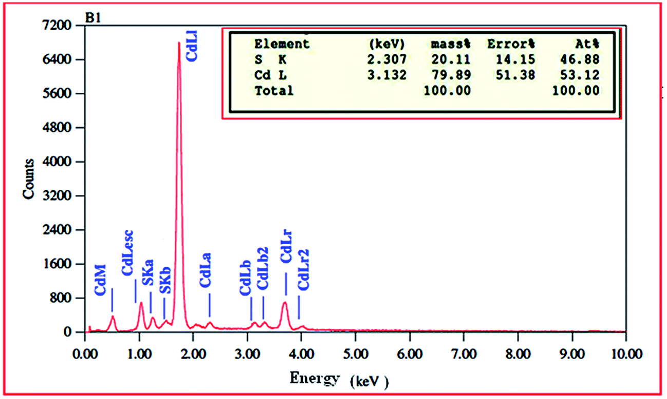
Energy dispersive X-ray (EDAX) spectroscopy was used to survey quantitatively chemical composition in atomic percentage of cadmium and sulfur in chemically deposited CdS thin films. A typical EDAX spectrum of as deposited CdS sample is presented in Fig. 3. EDAX spectrum analysis confirmed the existence of Cd and S elements in the deposited films and no noticeable impurity was observed.
 |
| | Fig. 3 EDAX spectrum of CdS thin film. | |
3.4. Scanning electron microscopy (SEM) analysis
The two-dimensional surface morphological studies of the CdS thin film was carried out using SEM technique and displayed in Fig. 4.The SEM image clearly shows the spherical shaped many small grains which are homogenously distributed over the substrate surface with some pores are between them. Such a granular porous morphology is useful for gas sensing application because the gas diffusion occurs more easily in porous structure and hence increases the reaction between gas molecules and the film surface results in the improvement of the gas sensing properties as well as porous morphology provides higher surface area to volume ratio, it means that such a film structure is likely to facilitate the adsorption process of gas molecules because of the larger surface area.26,27
 |
| | Fig. 4 SEM micrograph of CdS thin film. | |
3.5. Transmission electron microscopy (TEM) analysis
Transmission electron micrograph (TEM) and selected area electron diffraction (SAED) pattern of CdS thin film is shown in Fig. 5. The TEM image of CdS thin film in Fig. 5(a) shows that, interconnected spherical nanoparticles with an average particle size of 36 nm. Selected area electron diffraction pattern of the CdS thin film in Fig. 5(b) showed three clear diffraction rings, which corresponded to the (111), (220) and (331) planes of the cubic CdS respectively. This is in good agreement with the XRD analysis results and indicated that, the CdS nanoparticles are well crystallized.
 |
| | Fig. 5 (a) TEM and (b) SAED pattern of CdS thin film. | |
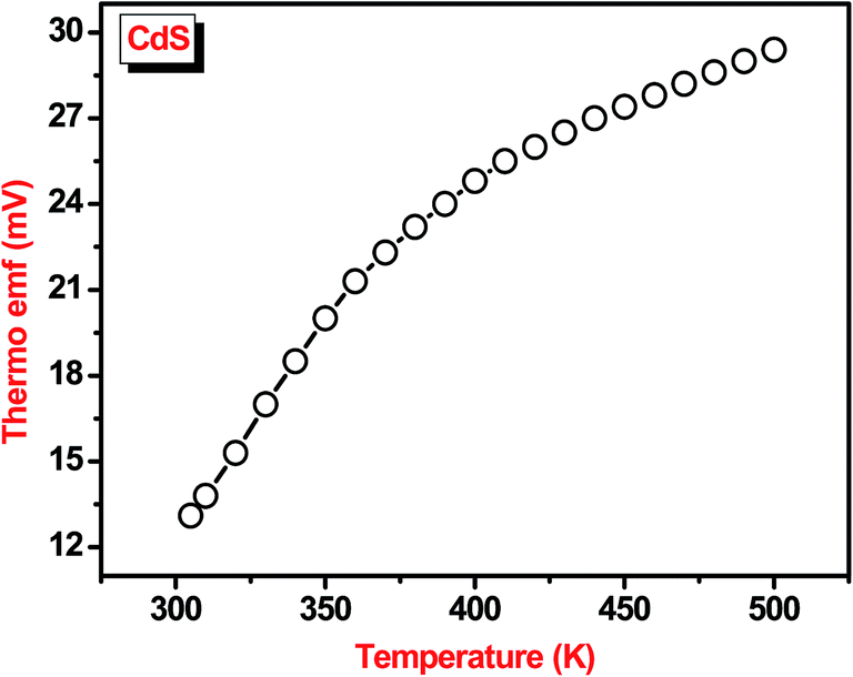
3.6. Thermoelectric power measurement
Thermoelectric power (TEP) measurement was carried out to confirm type of conductivity of chemical bath deposited CdS thin film. In TEP measurement, the temperature difference causes the transport of carriers from the hot end to cold end, which results in creates an electric field and gives thermo-emf across the hot and cold ends. Thermo-emf generated is directly proportional to the temperature gradient across the semiconductor. Type of conductivity was decided from the sign of thermo-emf generated across the hot and cold ends. The thermo-emf generated by the samples was measured in the 300–500 K temperature range and corresponding results are displayed in Fig. 6. The plot shows nonlinear variation in thermo-emf with increase in temperature from 300–500 K. In the present study, polarity of thermally generated voltage for chemically deposited CdS thin film is positive towards hot end with respect to cold end confirming the n-type conductivity of the film.12,14
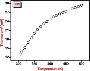 |
| | Fig. 6 Variation of thermo-emf with temperature for CdS thin film. | |
3.7. Gas sensing properties
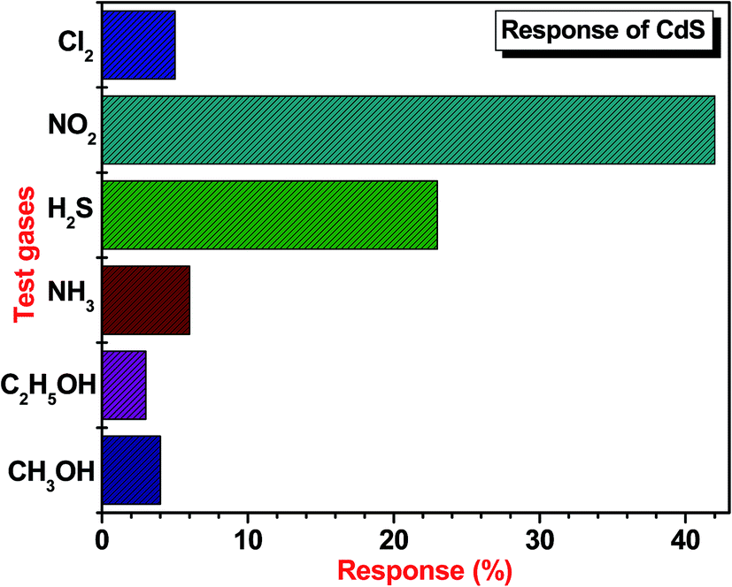
3.7.1. Selectivity study of CdS sensor. Room temperature (38 °C) gas sensing properties of the chemical bath deposited CdS thin film was investigated using two-probe resistance measurement set-up (shown in Fig. 1). Various kinds of test gases (each with a fixed concentration of 100 ppm) such as ammonia (NH3), nitrogen dioxide (NO2), hydrogen sulfide (H2S), ethanol (C2H5OH), methanol (CH3OH) and chloride (Cl2) were used for selectivity study. Fig. 7 shows bar chart for selectivity of CdS sensor towards various test gases. From Fig. 7 it is clearly seen that, CdS sensor shows different response for the different gases used. Theoretically, the sensors should have high response towards some gases but on the other hand, there is little or no response to other gases in the same surroundings. This may be due to the different gases have different energies for reaction to occur on the surface of sensor film.26 Fig. 7 shows that, CdS sensor exhibit a good response of 42% towards 100 ppm NO2 gas as compared to other test gases working at room temperature.
 |
| | Fig. 7 Selectivity of CdS sensor. | |
The selectivity coefficient (K) of NO2 gas to another gas is defined as,28
where,
SNO2 and
Sx are the sensitivities of sensor in NO
2 and other (X) gas.
The calculated values of selectivity coefficients are displayed in Table 1. The larger value of K means the sensor has a better ability to discriminate the NO2 gas amongst the mixture gases.
Table 1 K values of the sensor made by the thin film with CdS for the NO2 as a target gas
| Test gas |
NH3 |
C2H5OH |
Cl2 |
CH3OH |
H2S |
| K value |
7 |
14 |
5 |
10.5 |
1.82 |
Therefore, we could find that CdS sensor had a good sensing performance to NO2 gas. This may be due to the different gases have different energies for reaction to occur on the surface of sensor film. The plausible mechanism of selectivity for NO2 may be traced to the characteristics of vapor adsorbed over the surface of CdS film.
The higher response towards NO2 than NH3, H2S, C2H5OH, CH3OH and Cl2 can be explained on the basis of different interactions between sensing film and adsorbed gas. When CdS film interacts with reducing gases like NH3, H2S, C2H5OH and CH3OH, there is enhancement in charge carrier density due to electron donating nature of these gas. This results in increasing the conductivity of material and film resistance decreases. In case of oxidizing gas like NO2 and Cl2 there is a reduction in charge carrier concentration, since NO2 and Cl2 gas is electron accepting in nature. Hence it decreases the conductivity of the material. The interaction of NH3, H2S, C2H5OH, CH3OH and Cl2 with CdS film is very less as compared to NO2, hence it shows very less and sluggish response.
Thus from selectively results it is observed that, CdS sensor highly sensitive towards NO2 gas therefore, further dependence of NO2 response for CdS sensor is studied for various concentrations of NO2 gas operating at room temperature.
3.7.2. Response study of CdS sensor towards NO2 gas. In order to evaluate the lowest detection limit, we evaluated the response of CdS sensor for various concentrations of NO2 gas.The sensing capability of CdS sensor towards different concentrations (5–100 ppm) of NO2 gas has been explored. Fig. 8 shows electrical response of CdS film to 5–100 ppm of NO2. The resistance increases dramatically upon exposure to NO2 gas attains stable value and decreases gradually after being transferred to clean air. The increase in resistance after exposure to NO2 may be because of porous structure of CdS films leading to the predominance of surface phenomena over bulk material phenomena. The resistance attains stable value when dynamic equilibrium is attained .The response values of CdS sensor film is plotted as a function of NO2 concentration is shown Fig. 9. It is observed that the response saturates at higher concentration; this may be due to less availability of surface area with possible reaction sites on surface of the film. A good response time of 50 s and recovery time of 12 min is observed for CdS film exposed to a 100 ppm NO2.
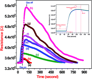 |
| | Fig. 8 Electrical response of CdS film with time for (a) 5 ppm, (b) 10 ppm, (c) 20 ppm, (d) 40 ppm, (e) 60 ppm, (f) 80 ppm, (g) 100 ppm and (h) 200 ppm NO2 gas (inset show NO2 response stabilization). | |
 |
| | Fig. 9 Dynamic response of CdS sensor for different concentrations of NO2. | |
Fig. 10 shows the relationship between response and various NO2 gas concentrations for the CdS sensor. From Fig. 8 it was observed that, CdS sensor exhibit linear response in the range of 5–100 ppm and above 200 ppm, the response of CdS sensor was remain constant, which indicates the sensor reaches saturation state at above 200 ppm. In the inorganic materials the gas sensing properties are largely governed through the surface reactions as well as via diffusion of target gases. A low NO2 gas concentration indicates that, a lower surface coverage of gas molecules which results into lower surface interaction between the surface and the NO2 gas molecules. As the concentration of NO2 gas increases then increases the interactions between the surface and the NO2 gas molecules due to a larger surface coverage. For further increase in NO2 gas concentration, the surface reactions get saturated and which leads to constant response. The maximum gas response of 61% was obtained for the exposure of 200 ppm of NO2 gas operating at room temperature. From the above results it was concluded that, the CdS sensor able to detect up low concentration (5 ppm) of NO2 gas operating at room temperature and the linearity in response in range of 5–100 ppm indicating the CdS can be used as promising materials to detect up the concentration of NO2 gas over this range.
 |
| | Fig. 10 Response of CdS sensor for different concentration of NO2 gas. | |
3.7.3. Sensing mechanism of CdS sensor towards NO2 gas. The gas sensing mechanism of CdS film and NO2 gas is demonstrated by a potential barrier model displayed in Fig. 11. The NO2 sensing mechanism of chemical bath deposited CdS film is demonstrated on the basis of change in the resistance of the CdS film. It is observed that, on exposure to NO2 gas molecules with CdS film showed the sudden increase in the resistance. Such a observed increased in the resistance of CdS film on interaction with NO2 gas molecules is due to the adsorption of gas on the surface of CdS thin film as well as the subsequent reactions between them. Generally, inorganic materials can adsorb oxygen from the air such as the O2−, O2− and O− species and change in resistance occurs due to adsorption of oxygen. The O2− adsorption is more reactive at room temperature therefore it makes the material more sensitive in the presence of an oxidizing gases (herein NO2). CdS is n-type semiconductor and when it interacts with oxidizing gases (electron accepter) like NO2 then adsorption of oxygen (in normal air) leads to removal of electrons. This leads to decrease in carrier concentration of CdS, which increases the height of potential barrier (ΦB). The overall reaction of NO2 gases molecules with adsorbed oxygen can explained as follows:| |
 | (8) |
| |
 | (9) |
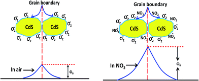 |
| | Fig. 11 Proposed schematic of interaction mechanism between CdS film and NO2 gas. | |
Since the majority carrier (electrons) density of CdS gets decreased due to electron accepting nature of NO2 gas it results in decrease in the conductivity of material and hence increasing sensors electrical resistance.
The attractive feature of the CdS thin film sensor is its room temperature operation, fast response time and the reproducible response characteristics. This may increase shelf life of sensor and makes it reusable.
3.7.4. Reproducibility and stability study of CdS sensor. The reproducibility study of the chemical bath deposited CdS thin film was measured by repeating the response measurement test three times. Fig. 12 shows the response of CdS thin film sensor upon periodic exposure to 100 ppm of NO2 gas working at room temperature. CdS sensor show good reproducible result upon repeated exposure and removal of NO2 gas at room temperature indicating excellent reproducibility and reversibility of sensor.
 |
| | Fig. 12 Reproducibility of CdS film to 100 ppm of NO2 gas. | |
Stability performance of CdS sensor was studied at room temperature upon exposure of fixed 100 ppm concentration of NO2 gas for 40 days at an interval of 5 days, after the first measurement and the results of gas response are explored in Fig. 13. Generally it is well known that, the common drawback of inorganic material based sensors is its decrease in response due to aging induced effects or humidity effects. Initially, CdS sensor exhibits higher response of 42% on exposure to 100 ppm of NO2 gas however it dropped from 42% to 29% as the time increased up to 40 days with 81% stability. From Fig. 13, it is seen that performance of sensor became stable after 15 days. From the reproducibility and stability study of chemical bath deposited CdS thin film it was concluded that such material with excellent gas sensing properties operating at room temperature may have potential application as NO2 gas sensor.
 |
| | Fig. 13 Stability study of CdS sensor. | |
The reproducibility and stability results are in consonance with reported literature on CuO as ethanol vapor sensor, niobium oxide as hydrogen gas sensor and tungsten trioxide nano rod thin-film sensors.29–31
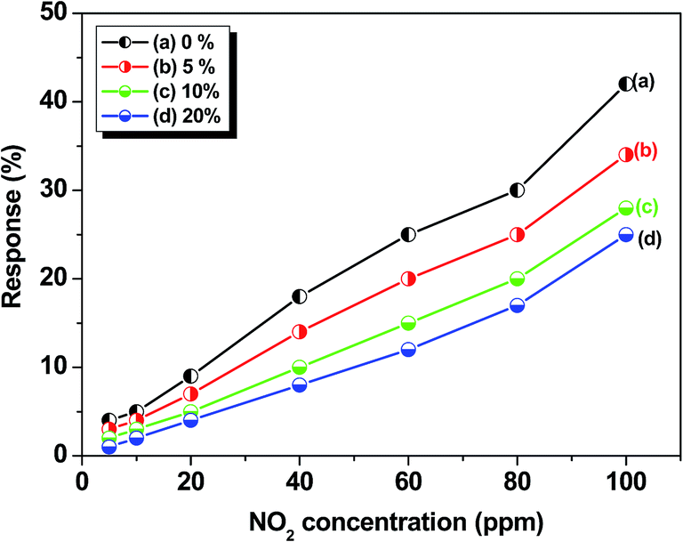
3.7.5. Effect of humidity on CdS sensor. Fig. 14 shows the response of CdS sensor with increase of NO2 concentration in gas composition with water vapors. The response of NO2 gradually decreased with the increase in water vapor could adsorb on the active sites of CdS film and prevent NO2 gas from adsorbing on the CdS films.
 |
| | Fig. 14 Effect of humidity on CdS sensor. | |
4. Conclusions
A novel NO2 gas sensor based on CdS thin film was successfully fabricated by chemical bath deposition method. The different chemical sensing behavior of the CdS thin films carried out at room temperature showed highest response (61%) towards NO2 gas (200 ppm) among various test gases. CdS sensor was able to detect up 5 ppm of NO2 gas and show linear relationship between the response and gas concentration in the range of 5–200 ppm towards NO2 gas. In addition, the cross response towards Cl2, NH3, C2H5OH and CH3OH was negligible leading to more reliable screening of NO2 gas. Moreover, the novel NO2 gas sensor had good stability and excellent reproducibility under room temperature conditions. The response and recovery times of the sensor were found to be quite fast as compared to other gases. The water vapor was completely adsorbed on the CdS film with NO2 gas.
All the gas sensing results demonstrate that, CdS thin films can be used for facile fabrication of high performance selective NO2 sensors working at room temperature.
Acknowledgements
Authors (VBP) are grateful to DAE-BRNS, for financial support through the scheme no. 2010/37P/45/BRNS/1442. This research was also supported by the New & Renewable Energy of the Korea Institute of Energy Technology Evaluation and Planning (KETEP) grant funded by the Korean government's Ministry of Trade, Industry and Energy (no. 20123010010130).
References
- J. F. Mcaleer, P. T. Moseley, J. O. W. Norris, D. E. Williams, P. Taylor and B. C. Tofield, “Tin oxide based gas sensors”, Mater. Chem. Phys., 1987, 17, 577 CrossRef CAS.
- M. Di Giulio, G. Micocci, A. Serra, A. Tepore, R. Rella and P. Siciliano, “SnO2 thin films for gas sensor prepared by r.f. reactive sputtering”, Sens. Actuators, B, 1995, 24, 465 CrossRef.
- Y. Shimizu and M. Egashira, “Basic aspects and challenges of semiconductor gas sensors”, Mater. Res. Bull., 1999, 6, 18 CrossRef.
- C. Pijolat, C. Pupier, M. Sauvan, G. Tournier and R. Lalauze, “Gas detection for automotive pollution control”, Sens. Actuators, B, 1999, 59, 195 CrossRef CAS.
- V. E. Bochenkov and G. B. Sergeev, “Preparation and chemiresistive properties of nanostructured materials”, Adv. Colloid Interface Sci., 2005, 116, 245 CrossRef CAS PubMed.
- S. T. Navale, D. K. Bandgar, S. R. Nalage, G. D. Khuspe, M. A. Chougule, Y. D. Kolekar, S. Sen and V. B. Patil, “Synthesis of Fe2O3 nanoparticles for nitrogen dioxide gas sensing application”, Ceram. Int., 2013, 39, 6453 CrossRef CAS PubMed.
- G. D. Khuspe, R. D. Sakhare, S. T. Navale, M. A. Chougule, R. N. Mulik, R. C. Pawar, C. S. Lee and V. B. Patil, “Nanostructured SnO2 thin film for NO2 gas sensing applications”, Ceram. Int., 2013, 39, 8673 CrossRef CAS PubMed.
- S. Bose and S. K. Saha, “Synthesis and Characterization of Hydroxyapatite Nanopowders by Emulsion techniques”, Chem. Mater., 2003, 15, 4464 CrossRef CAS.
- A. Bauger, J. C. Mutin and J. C. Niepce, “Synthesis reaction of metatitanate BaTiO3”, J. Mater. Sci., 1983, 18, 3041 CrossRef.
- T. L. Chu and S. S. Chu, “High efficiency thin films CdS/CdTe solar cells”, Int. J. Sol. Energy, 1992, 12, 121 CrossRef.
- J. Britt and C. Ferekides, “Thin film CdS/CdTe solar cell with 15.8% efficiency”, Appl. Phys. Lett., 1993, 62, 2851 CrossRef CAS PubMed.
- V. B. Patil, D. S. Sutrave, G. S. Shahane and L. P. Deshmukh, “Cadmium telluride thin films: growth from solution and characteristics”, Thin Solid Films, 2001, 401, 35 CrossRef CAS.
- V. B. Patil and L. P. Deshmukh, “Photoelectrochemical investigations on n-CdS1−x Tex thin film electride/polysulphide system”, Int. J. Electron., 2004, 13, 91 Search PubMed.
- B. T. Raut, P. R. Godse, S. G. Pawar, M. A. Chougule and V. B. Patil, Development of nanostructured CdS sensor for H2S recognition: structural and physical characterization, J. Mater. Sci: Mater. Electron, 2012, 23, 956–963 CrossRef CAS.
- T. Arai, T. Yoshida and T. Ogawa, “Photoacoustic and Luminescence spectra of CdS fine particles”, J. Appl. Phys., 1987, 26, 396 CrossRef CAS.
- O. V. Salata, P. J. Dobson, P. J. Hull and J. L. Hutchinson, “Fabrication of CdS nanoparticles embedded in polymer film by gas aerosol reactive electrostatic deposition technique”, Thin Solid Films, 1994, 251, 1 CrossRef CAS.
- H. H. Afify and I. K. Battisha, “Oxygen interaction with CdS based gas sensors by varying different preparation parameters”, J. Mater. Sci.: Mater. Electron., 2000, 11, 373–377 CrossRef CAS.
- R. Demir, S. Okur and M. Şeker, “Electrical characterization of CdS nanoparticles for humidity sensing applications”, Ind. Eng. Chem. Res., 2012, 51(8), 3309–3313 CrossRef CAS.
- H. Xia, J. Peng, K. Liu, C. Li and Y. Fang, “Preparation and gas sensing properties of Novel CdS-supramolecular organogel hybrid films”, J. Phys. D: Appl. Phys., 2008, 41, 105405 CrossRef.
- D. S. Dhawale, D. P. Dubal, V. S. Jamadade, R. R. Salunkhe, S. S. Joshi and C. D. Lokhande, “Room temperature LPG sensor based on n-CdS/p-polyaniline heterojunction”, Sens. Actuators, B, 2010, 145, 205–210 CrossRef CAS PubMed.
- J. Zhai, L. Wang, D. Wang, H. Li, Y. Zhang, D. He and T. Xie, “Enhancement of gas sensing properties of CdS nanowire/ZnO nanosphere composite materials at room temperature by visible-light activation”, ACS Appl. Mater. Interfaces, 2011, 3, 2253–2258 CAS.
- X. Fu, J. Liu, Y. Wan, X. Zhang, F. Meng and J. Liu, “Preparation of a and its enhanced gas-sensing properties for detecting volatile organic compounds”, Mater. Chem. Phys., 2012, 22, 17782–17791 CAS.
- M. Karimi, M. Rabiee, F. Moztarzadeh, M. Tahriri and M. Bodaghi, “Controlled synthesis, characterization and optical properties of CdS nanocrystalline thin films via chemical bath deposition route”, Curr. Appl. Phys., 2009, 9, 1263 CrossRef PubMed.
- R. Jayakrishnan, J. P. Nair, B. A. Kuruvilla, S. K. Kulkarni and R. K. Pandey, “Composition, structure and morphology of dip coated rapid thermal annealed CdS and nonaqueous electrodeposited CdTe”, Semicond. Sci. Technol., 1996, 11, 116 CrossRef CAS.
- P. N. Gibson, M. E. O. Zsan, D. Lincot, P. Cowache and D. Summa, “Modelling of substrate of CdS thin films”, Thin Solid Films, 2000, 361, 34 CrossRef.
- S.T. Navale, A. T. Mane, M. A. Chougule, R. D. Sakhare, S. R. Nalage and V. B. Patil, Highly selective and sensitive room temperature NO2 gas sensor based on polypyrrole thin films, Synth. Met., 2014, 189, 94–99 CrossRef CAS PubMed.
- X. W. Lou, L. A. Archer and Z. Yang, “Micro-/Nanostructures: Synthesis and Applications, Adv. Mater., 2008, 20, 3987 CrossRef CAS.
- S. L. Patil, S. G Pawar, A. T. Mane, M. A. Chougule and V. B. Patil, J. Mater. Sci.: Mater. Electron., 2010, 21, 1332–1336 CrossRef CAS.
- A. S. Zoolfakar, M. Z. Ahmad, R. A. Rani, J. Z. Ou, S. Balendhran, S. Zhuiykov, K. Latham, W. Wlodarski and K. Kalantar-zadeh, Sens. Actuators, B, 2013, 185, 620–627 CrossRef CAS PubMed.
- R. A. Rani, A. S. Zoolfakar, J. Z. Ou, M. R. Field, M. Austin and K. Kalantar-zadeh, Sens. Actuators, B, 2013, 176, 149–156 CrossRef CAS PubMed.
- M. Z. Ahmad, A. Wisitsoraat, A. S. Zoolfakar, R. A. Kadir and W. Wlodarski, Sens. Actuators, B, 2013, 183, 364–371 CrossRef CAS PubMed.
|
| This journal is © The Royal Society of Chemistry 2014 |
Click here to see how this site uses Cookies. View our privacy policy here.