
Structural, electrical and optical properties of Mg-doped CuAlO2 films by pulsed laser deposition
Y. S. Zou*,
H. P. Wang,
S. L. Zhang,
D. Lou,
Y. H. Dong,
X. F. Song and
H. B. Zeng*
School of Materials Science and Engineering, Institute of Optoelectronics & Nanomaterials, Nanjing University of Science and Technology, Nanjing, Jiangsu 210094, China. E-mail: yshzou75@gmail.com; zeng.haibo@njust.edu.cn; Fax: +86 25 84303279
First published on 28th August 2014
Abstract
CuAl1−xMgxO2 (x = 0, 0.01, 0.02, 0.05) films were deposited on sapphire and fused silica substrates by pulsed laser deposition and underwent annealing in an Ar atmosphere at the temperature of 1000 °C. The effects of Mg concentration on the structural, morphological, electrical and optical properties were investigated by X-ray diffraction (XRD), X-ray photoelectron spectroscopy (XPS), scanning electron microscopy (SEM), UV-visible-NIR spectrophotometry and a Hall effect measurement system. The results indicate that Mg is successfully doped into the CuAlO2 film with p-type conduction after annealing. Single and pure-phase CuAl1−xMgxO2 (x = 0, 0.01, 0.02, 0.05) films with c-axis orientation are obtained on sapphire substrates in the studied doping range, and a secondary phase is not detected by XRD measurements. The substitution of Mg2+ ions in Al3+ sites induces lattice distortion and results in the decline of the crystalline quality. The Hall effect measurement reveals that the carrier concentration increases and Hall mobility decreases with the increase of Mg doping concentration. The resistivity of the CuAl1−xMgxO2 films decreases and then increases with increasing Mg doping concentration from 0 to 5%. The minimum resistivity of 11.45 Ω cm is obtained at room temperature for the CuAl1−xMgxO2 films with x = 2%. The optical transmittance gradually reduces with the increase of Mg concentration due to the enhancement of absorption of incident photons. The optical band gaps of CuAl1−xMgxO2 films are found to decrease from 3.54 to 3.43 eV as the Mg doping concentration increased from 0 to 5% due to the formation of impurity energy levels.
1. Introduction
As a promising material attracting much attention, both n-type and p-type transparent conducting oxides (TCOs) have been used as transparent electrodes for electronics technology, such as solar cells,1 transistors,2 photodetectors,3 and light-emitting diodes,4,5 owing to their functional combination of transparency and electrical conductivity. However, most of the known TCOs are n-type semiconductor materials,6–8 such as tin oxide, zinc oxide, indium oxide and cadmium oxide, no p-type TCOs were found until the report of the delafossite-type CuAlO2 fabricated by Kawazoe9 using the pulsed laser deposition method in 1997. Many efforts have been devoted so far to fabricate p-type CuAlO2 and numerous studies on the improvement of optical and electrical properties of the deposited CuAlO2 films have been carried out.10–14 Unfortunately, some difficulties, including high crystallization temperature, introduction of secondary phase and low conductivity were encountered for the deposited CuAlO2 films.15,16 Post-annealing treatment in N2 or Ar atmosphere as an important and very effective technique has been employed to yield crystalline CuAlO2 films and improve the structural properties. Lan et al. found that the crystallinity of CuAlO2 films deposited by magnetron sputtering was improved with increasing the annealing temperature in a N2 atmosphere, and the annealed film showed the preferred c-axis orientation.17 Compared to n-type TCOs, both conductivity and transparency of the reported p-type TCOs are still significantly inferior, especially for the conductivity of CuAlO2 film which is three or four orders of magnitude lower than that of popular n-type TCOs, which have limited the applications of CuAlO2 films in photovoltaic cells, gas sensors, light-emitting diodes and transistors. Therefore, improving the electrical properties of CuAlO2 film and manufacturing pure-phase CuAlO2 film seem to be necessary for practical applications and are an important issue.CuAlO2 with a wide direct band gap of 3.5 eV at room temperature has an ABO2 delafossite structure. Therefore, the substitution of bivalent cations in B sites is generally considered as a direct and effective route to increasing electrical conductivity. Recently, considerable efforts have been made to improve the properties of Cu-based delafossites by using the doping technology, such as Mg/Mn/Ca/Zn-doped CuAlO2/CuScO2/CuCrO2/CuYO2.18–21 Nagarajan et al. reported the Mg-doped CuCrO2 film prepared by RF sputtering with a conductivity of 220 S cm−1 and found that the optimal value for doping was 5 at%.18 However, the optical transmittance in the visible region of CuCr1−xMgxO2 film is in the range of only 30–40%. Zhu et al. found that substituting Al3+ in the CuAlO2 film deposited by chemical solution method with Mg2+ increases the transmittance in the visible region and electrical conductivity. The conductivity of the 1 at% Mg-doped CuAlO2 film is up to 5.2 × 10⁻³ S cm−1 at 300 K.22 Dong et al. reported that the conductivity of the CuAlO2 film deposited by RF magnetron sputtering exhibited notable improvement through Mg doping, and the conductivity of the CuAl0.98Mg0.02O2 film is three orders of magnitude higher than that of undoped CuAlO2 film.23
So far, several growth methods, such as pulsed laser deposition (PLD),9,24 chemical vapor deposition (PECVD),25 electron beam evaporation,26 magnetron sputtering,17,27–29 sol–gel30 and spraypyrolysis,31 have been applied to grow CuAlO2 films. Among those methods, pulsed laser deposition technique has been considered largely for the growth of device quality films and is promising in preparing CuAlO2 films over the traditional deposition methods due to its several advantages, including good adhesion to the substrate, reproducibility and controllability of stoichiometry and crystal structure, and the easy deposition of alloys and compounds of materials with different vapor pressures. Therefore, PLD is beneficial to the deposition of CuAlO2 film. However, the effect of Mg content on the properties of CuAlO2 films deposited by PLD is less studied. In this study, Mg-doped CuAlO2 films were deposited on sapphire substrates by PLD. Then, the deposited films were conducted the annealing treatment in Ar ambient to improve the phase purity and crystallinity. The influence of Mg substitution on the structural, electrical and optical properties of Mg-doped CuAlO2 films is systematically investigated.
2. Experimental
Polycrystalline targets of CuAl1−xMgxO2 (x = 0, 0.01, 0.02, 0.05) were prepared by a conventional solid-state reaction. Stoichiometric amounts of high purity Cu2O, Al2O3 and MgO were carefully mixed. Then the reactants were calcined at 1150 °C for 10 hours to generate CuAl1−xMgxO2 (x = 0, 0.01, 0.02, 0.05) powders. After ball milling for 6 hours, the calcined powders were pressed into disk as the target, and sintered at 1150 °C for 4 hours. Then the ceramic targets for PLD were obtained.The Mg-doped CuAlO2 films were grown on (0001) sapphire and fused silica by PLD using the calcined disk target. The substrates were cleaned sequentially with acetone, ethanol, and deionized water in an ultrasonic cleaner. The distance between substrate and target was 60 mm. Prior to deposition, the chamber was pumped down to 10−3 Pa by rotary pump and molecular pump. The target rotated continuously at 10 rpm was ablated with KrF excimer laser at laser energy of 230 mJ and frequency of 5 Hz. The high-purity oxygen was introduced into the chamber to maintain the pressure of 15 Pa during the film deposition. The Mg-doped CuAlO2 films were deposited at the substrate temperature of 650 °C for 60 min in an ambient with the oxygen partial pressure of 15 Pa. After deposition, all the deposited CuAl1−xMgxO2 films were post-annealed in a tube furnace under Ar atmosphere at the temperature of 1000 °C for 30 min.
The microstructure, crystal orientation, elementary composition and chemical bonding of the deposited and annealed CuAl1−xMgxO2 films were investigated by X-ray diffraction (XRD) and X-ray photoelectron spectroscopy (XPS) with a monochromatized Al Kα X-ray source. The surface morphology of the films was characterized by scanning electron microscopy (SEM). The optical properties of the films were characterized using UV-visible-NIR spectrophotometer. The electrical properties of the CuAl1−xMgxO2 films (x = 0, 0.01, 0.02, 0.05) were examined by the four-probe van der Pauw method at room temperature using Hall effect measurement system (Nanometrics HL5500PC). A permanent magnet is applied and the magnetic field strength is 0.5 T.
3. Results and discussion
Fig. 1 shows the XRD pattern of sintered CuAl1−xMgxO2 (x = 0, 0.01, 0.02, 0.05) targets prepared by a conventional solid-state reaction. For the undoped sintered target, all the diffraction peaks of CuAlO2 target without Mg doping can be identified as delafossite structure CuAlO2, and are consistent with the standard JCPDF card (no. 75-2361, space group R![[3 with combining macron]](https://www.rsc.org/images/entities/char_0033_0304.gif) m). No any peaks which belong to the starting materials or impurity phase are observed. The second phase of CuO and CuAl2O4 can be observed when the Mg dopant is introduced into the sintered targets. However, the MgO phase is not presented in all CuAl1−xMgxO2 targets from the XRD patterns. Moreover, with the increase of Mg content, more peaks of impurity phase appear, along with the enhanced intensity of second phase peak. This indicates that the Mg doping results in the decomposition of CuAlO2 phase32 via the following reaction:
m). No any peaks which belong to the starting materials or impurity phase are observed. The second phase of CuO and CuAl2O4 can be observed when the Mg dopant is introduced into the sintered targets. However, the MgO phase is not presented in all CuAl1−xMgxO2 targets from the XRD patterns. Moreover, with the increase of Mg content, more peaks of impurity phase appear, along with the enhanced intensity of second phase peak. This indicates that the Mg doping results in the decomposition of CuAlO2 phase32 via the following reaction:| 4CuAlO2 + O2 = 2CuO + 2CuAl2O4 | (1) |
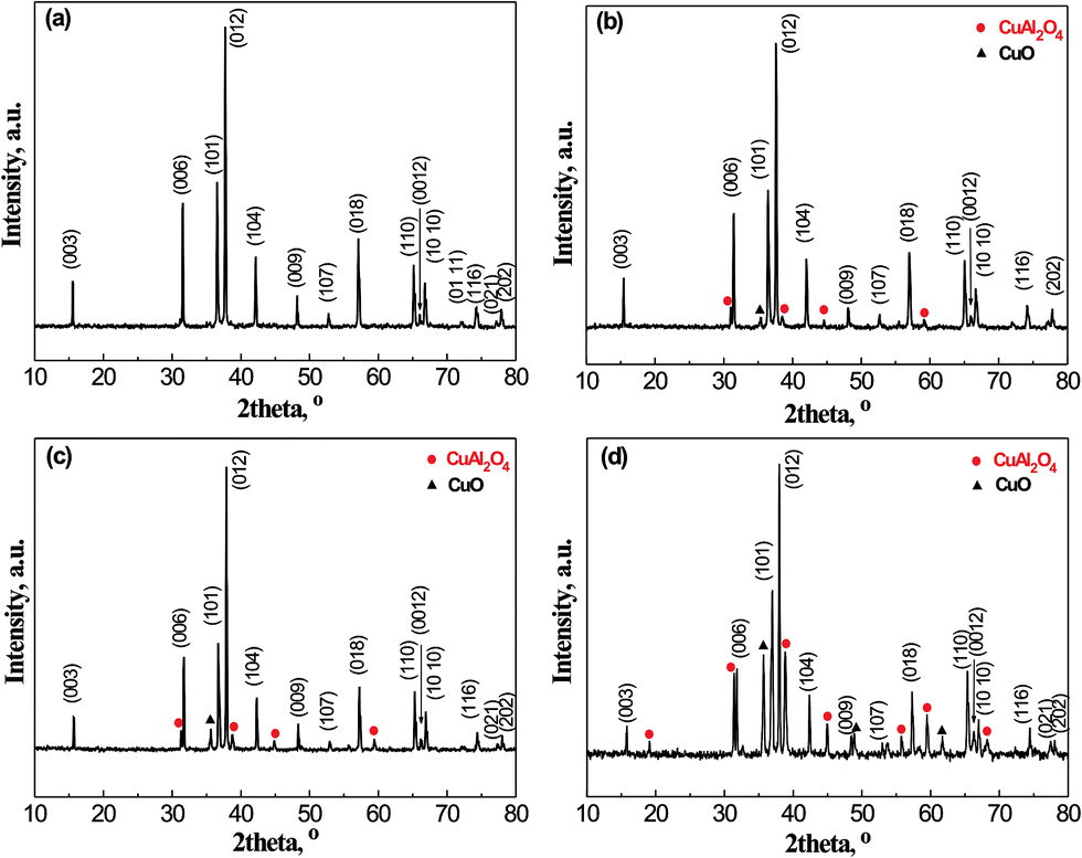 | ||
| Fig. 1 XRD patterns of Mg-doped CuAlO2 target, (a) CuAlO2, (b) CuAl0.99Mg0.01O2, (c) CuAl0.98Mg0.02O2, (d) CuAl0.95Mg0.05O2. | ||
The as-deposited CuAl1−xMgxO2 films exhibit the amorphous structure at the substrate temperature of 650 °C. It is well known that the annealing is a very effective method to improve the crystalline of materials. Therefore, the annealing technique is employed for all the as-deposited CuAl1−xMgxO2 films by PLD to develop its electrical and optical properties. Fig. 2 shows the XRD patterns of the CuAl1−xMgxO2 films with various Mg compositions annealed in Ar atmosphere at the temperature of 1000 °C for 30 min. The annealing atmosphere of Ar acting as protective atmosphere is applied to avoid the decomposition of CuAlO2 films during the high temperature annealing. It can be seen that the annealed CuAl1−xMgxO2 films exhibit good crystallization and phase-pure. All the peaks are identified to be the reflections of CuAlO2 phase of the delafossite structure without any diffraction peak corresponding to the second phase presented after the annealing treatment, which is different from the XRD patterns of Mg-doped CuAlO2 target. This indicates that the introduction of Mg into CuAlO2 can't induce the impurity phases after annealing treatment. Meanwhile, the notable peaks corresponding to crystal plane of (003), (006), (009), (104) and (0012) indicate that the CuAl1−xMgxO2 (x = 0, 0.01, 0.02, 0.05) films are preferentially oriented along the c-axis perpendicular to the substrate surface. This c-axis orientation growth suggests that the surface energy of the (001) family of crystal plane could be the lowest in CuAlO2 crystal. Thus it can be proved that the annealing treatment in Ar atmosphere is beneficial for the formation of pure phase CuAlO2 and (001) orientation growth. However, the intensities of diffraction peaks of CuAl1−xMgxO2 films decrease with increasing Mg concentration, meanwhile (0012) peak appears when the Mg concentration increases up to 5 at%, which reflects the weakened c-axis orientation growth. The decline of the crystalline quality of CuAl1−xMgxO2 films may be due to the substitution of Mg2+ for Al3+.
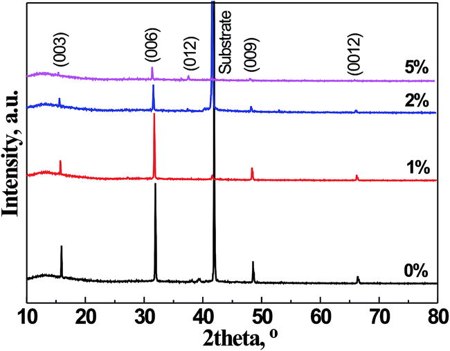 | ||
| Fig. 2 XRD patterns of annealed CuAl1−xMgxO2 (x = 0, 0.01, 0.02, 0.05) films. | ||
As seen in Fig. 2, the (006) peaks for all the CuAl1−xMgxO2 (x = 0, 0.01, 0.02, 0.05) films shift toward lower angles with the increase of Mg content, which subsequently inferring to the variation of lattice constants c shown in Fig. 3. It can be seen that the lattice constant c of CuAl1−xMgxO2 films gradually increases with increasing the Mg-doping concentration, which reflects the fact of crystal cell expansion. The cell expansion can be ascribed to the substitution of Mg for Al in the CuAlO2 lattice to form substitutional solid solution. Due to the mismatch between the ionic radii, the substitution of Mg2+ (0.066 nm) ions in Al3+ (0.051 nm) sites induces lattice distortion, which consequently results in the decline of the crystalline quality.
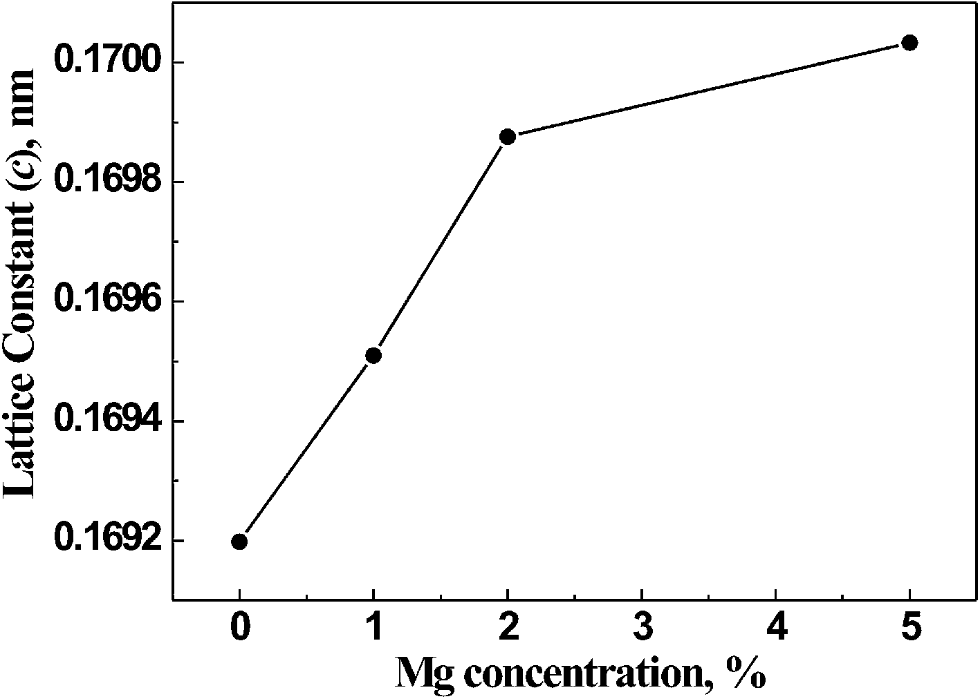 | ||
| Fig. 3 Lattice constant (c) of annealed CuAl1−xMgxO2 (x = 0, 0.01, 0.02, 0.05) films. | ||
To further identify the chemical compositions and valences of the elements, XPS analysis was performed to characterize the annealed CuAl1−xMgxO2 (x = 0, 0.01, 0.02, 0.05) films. Fig. 4 shows the XPS wide survey spectra of CuAl1−xMgxO2 (x = 0, 0.01, 0.02, 0.05) films annealed in Ar atmosphere at the temperature of 1000 °C for 30 min. It can be observed that the spectrum of the undoped CuAlO2 is dominated by C1s, O1s, Cu2p and Al2p peak. The carbon signal perhaps originates from the XPS measurement system. For all the Mg doped CuAlO2 films, the Mg2s signal in the XPS spectra appears, indicating that Mg is successfully doped into the CuAlO2 films. High-resolution XPS scans were acquired for the O1s, Cu2p, Al2p and Mg2s regions of the CuAl1−xMgxO2 films with x = 5%, as shown in Fig. 5. Fig. 5(a) shows the Cu2p core spectrum with the binding energy of Cu2p3/2 at about 931.8 eV and Cu2p1/2 at about 950.9 eV. There is no shake-up line of Cu2p3/2 between peak of Cu2p3/2 and Cu2p3/1 in the spectrum. The absence of shake-up implies that the valence state of Cu in CuAl0.95Mg0.05O2 film is Cu+. It is well established that the core level spectrum of Cu2+ compounds has a strong shake-up satellite feature which is absent in the core level spectra of Cu+ compounds.33 This feature has been widely used for the identification of different oxidation states of copper in various copper compounds. The absence of satellite peaks suggests that valence state of Cu in CuAl0.95Mg0.05O2 film is Cu+. This is confirmed in other samples with various Mg doping concentrations as well, which suggests that impurity phases of CuO and CuAl2O4 can be eliminated after annealing treatment. XPS studies along with XRD results indicate that there is only CuAlO2 phase in our samples. Based on the integral intensity of O1s, Cu2p, Al2p and Mg2s peaks, and the intrinsic sensitivity factors of oxygen, copper, aluminum and magnesium, the actual Mg doping contents are calculated to be 0.96%, 1.83%, 4.86% for the film CuAl0.99Mg0.01O2, CuAl0.98Mg0.02O2 and CuAl0.95Mg0.05O2, respectively.
 | ||
| Fig. 4 The XPS wide survey spectra of annealed CuAl1−xMgxO2 (x = 0, 0.01, 0.02, 0.05) films, (a) CuAlO2, (b) CuAl0.99Mg0.01O2, (c) CuAl0.98Mg0.02O2, (d) CuAl0.95Mg0.05O2. | ||
 | ||
| Fig. 5 XPS spectra of annealed CuAl0.95Mg0.05O2 film, (a) local fine scanning of Cu, (b) local fine scanning of A12p and Cu3p after fitting, (c) local fine scanning of O1s, (d) local fine scanning of Mg2s. | ||
Fig. 6 shows the surface morphologies of the obtained CuAl1−xMgxO2 films with various Mg doping concentrations annealed in Ar atmosphere at the temperature of 1000 °C for 30 min. For the deposition without Mg doping, the undoped CuAlO2 film exhibits continuous, dense and granular structure morphology without obvious micro-cracks. The surface of films is relatively smooth, and the grain size is homogeneous. Then the surface pattern varies with the introduction of Mg into the CuAlO2 film. With the increase of Mg doping concentration, the particles grow up gradually. Compared to the undoped CuAlO2 film, the CuAl0.95Mg0.05O2 film surface has an obviously larger grain except for some micro-holes, which suggests the decrease of grain boundaries.
 | ||
| Fig. 6 SEM images of the surface morphology of the annealed CuAl1−xMgxO2 films, (a) CuAlO2, (b) CuAl0.99Mg0.01O2, (c) CuAl0.98Mg0.02O2, (d) CuAl0.95Mg0.05O2. | ||
The Hall effect measurement is carried out to characterize the electrical properties of CuAl1−xMgxO2 films (x = 0, 0.01, 0.02, 0.05) at room temperature using the van der Pauw method.34 The Hall coefficients derived from the Hall measurement for CuAl1−xMgxO2 films with x = 0%, 1%, 2% and 5% are 40.76, 14.6, 6.82 and 5.02 m3 C−1, respectively. The positive Hall coefficient measured for these films verifies the p-type conduction behavior, indicating that the obtained CuAl1−xMgxO2 films are p-type semiconductor. Fig. 7 shows the variation of electrical performance parameters (carrier concentration, mobility, and resistivity) of CuAl1−xMgxO2 films with the increase of Mg doping concentration. The Hall effect measurement reveals the carrier concentration to be 2.70 × 10¹⁷, 7.71 × 10¹⁷, 1.69 × 10¹⁸ and 2.21 × 1018 cm−3 for CuAl1−xMgxO2 films with x = 0%, 1%, 2% and 5%, respectively. The increase of Mg doping concentration results in carrier concentration increasing, as shown in Fig. 7(a). The p-type conductivity in Cu+-based delafossites is dominated by d-orbital in Cu+(3d10) with charge compensation of the Cu2+(3d9). Bivalent cations, such as Mg2+, Ca2+, and Zn2+, doped onto Al3+ sites in CuAlO2 with layered structure semiconductor can increase p-type conductivity mainly by contributing to the hole concentration.35,36 In the Mg-doped CuAlO2 films, more holes can be formed by a charge-compensating mechanism when Mg2+ substitutes for Al3+, which in turn results in the enhancement of p-type conduction. This has been verified in delafossite structure by many reports, such as Mg doped CuCrO2 (ref. 37) and Mg-doped CuFeO2.38
 | ||
| Fig. 7 Variation of electrical performance parameter of annealed CuAl1−xMgxO2 (x = 0, 0.01, 0.02, 0.05) films, (a) carrier concentration, (b) Hall mobility, (c) electrical resistivity. | ||
In addition to the hole carrier concentration, Hall mobility is another significant factor that influences conductivity. By contrast, the Hall mobility decreases from 8.14 to 0.78 cm2 V−1 s−1 as Mg concentration increases from 0 to 5%, as shown in Fig. 7(b). The results can be attributed to the weakened c-axis orientation growth and the effect of the grain boundary scattering. According to the XRD results shown in Fig. 2, Mg doping is harmful to the preferred c-axis orientation of the CuAlO2 film. Consequentially the lowest Hall mobility of 0.78 cm2 V−1 s−1 is obtained when the Mg content is further increased to 5%. The film conductivity is determined by the product of carrier mobility and carrier concentration. Combining the measured carrier mobility and carrier concentration, the resistivity of the film is obtained, as shown in Fig. 7(c). It can be clearly seen that the average resistivity of the CuAl1−xMgxO2 films decreases from 16.67 to 11.45 Ω cm as Mg concentration increases from 0 to 2%, and then increases to 20.87 Ω cm when Mg concentration further increases to 5%. The highest conductivity is obtained for the CuAl1−xMgxO2 films with x = 2%, which is similar to the reported results for the CuAl1−xMgxO2 films deposited by RF magnetron sputtering.23 The increase of resistivity for the CuAl1−xMgxO2 films with x = 5% is a result of the increase of the carrier concentration and the decrease of mobility, and is mainly attribute to the lowest Hall mobility of 0.78 cm2 V−1 s−1. Moreover, the deposited amorphous CuAl1−xMgxO2 films before annealing were highly resistant and their electrical properties were not able to be characterized by the Hall effect measurement. Those results demonstrate that the combination of annealing technique and Mg doping is advantageous for enhancing the electrical conduction of CuAlO2 film.
The optical transmission spectra of CuAl1−xMgxO2 (x = 0, 0.01, 0.02, 0.05) films are investigated by UV-vis spectrophotometer. Fig. 8 shows the optical transmittance of the obtained CuAl1−xMgxO2 films in the range of 200–800 nm. As can be seen, the absorption edges for all the films can be clearly observed and the transmittance of Mg-doped CuAlO2 films decreases with the increment of Mg doping concentration. Compared with the Mg-doped CuAlO2 films, the undoped CuAlO2 film exhibits a relatively high transparence of over 85% in the visible light range. For the CuAl1−xMgxO2 film with x = 5%, the transmittance decreases to be about 45%. The optical transmittance gradually reduces with the increase of Mg concentration. The carrier concentration increases and carrier mobility decreases with the increase of Mg concentration in Mg-doped CuAlO2 films, as demonstrated in Fig. 7. Increasing carrier concentration and decreasing carrier mobility result in the enhancement of absorption of incident photons.39,40 The scattering and absorption of photons in the film resulting from doping lead to the reduction of the optical transmittance.41
 | ||
| Fig. 8 The room temperature UV-visible transmittance spectra of the annealed CuAl1−xMgxO2 (x = 0, 0.01, 0.02, 0.05) films. | ||
The optical band gap of the annealed CuAl1−xMgxO2 (x = 0, 0.01, 0.02, 0.05) films can be deduced by Tauc's relation expresses as (αhv)2 = C(hv − Eg)42 where C is a constant that depends on the electron–hole mobility, hν is the incident photon energy, Eg is the optical band gap, and α is the absorption coefficient, which is obtained near the absorption edge from the transmittance. The graph of (αhv)2 vs. hν is plotted to estimate the optical band gap of CuAl1−xMgxO2 films, as shown in Fig. 9. By extrapolating the straight portion of the curve, the direct optical band gap is estimated to be 3.54, 3.52, 3.49 and 3.43 eV for the sample of CuAl1−xMgxO2 films with x = 0, 1%, 2% and 5%, respectively. It is obvious that the Eg of CuAl1−xMgxO2 films decreases with increasing the Mg doping concentration, which is in good agreement with the similar results reported by Bhandari.43 The distortion of the CuO4 tetrahedra is increased after introducing Mg2+ into the lattice, which can cause the dispersion at VBM (valence-band maximum). Therefore, the 3d symmetry of Cu is degraded from D2d into a less symmetrical condition, causing less degenerate Cu 3d states, which makes the VBM increase slightly, consequently resulting in a narrower band gap.44 Beyond that, the increase of impurities and defects with increasing Mg doping concentration will generate the impurity energy levels, which effectively reduces the optical band gaps of Mg doped CuAlO2 films.23,45
 | ||
| Fig. 9 The relationship between (αhv)2 and photo energy (hv) for the annealed CuAl1−xMgxO2 (x = 0, 0.01, 0.02, 0.05) films. | ||
4. Conclusions
Single-phase high conductivity transparent p-type delafossite Mg doped CuAlO2 films were successfully deposited on sapphire and fused silica substrates by pulsed laser deposition followed by annealing at temperature of 1000 °C in Ar ambient. The dependence of structural, morphological, electrical and optical properties on Mg doping concentration was found. X-ray diffraction results reveal that the annealed CuAl1−xMgxO2 (x = 0, 0.01, 0.02, 0.05) films exhibit c-axis orientation without detected secondary phase, and that Mg substitution on Al sites results in lattice distortion and decline of the crystalline quality. The hole concentration increases from 2.70 × 10¹⁷ to 2.21 × 1018 cm−3 and Hall mobility decreases from 40.76 to 5.02 m3 C−1 for the CuAl1−xMgxO2 films as the Mg doping concentration increases from 0 to 5%. The optimum Mg doping concentration of 2% is achieved with the minimum resistivity of 11.45 Ω cm at room temperature. With the increase of Mg doping concentration, the optical transmittance is gradually reduced, and the optical band gaps of CuAl1−xMgxO2 films are found to decrease from 3.54 to 3.43 eV. Those results demonstrate that the combination of annealing technique and Mg doping is advantageous for enhancing the electrical conduction of CuAlO2 film.Acknowledgements
This work was financially supported by the Natural Science Foundation of Jiangsu Province of China (BK20141401), the Fundamental Research Funds for the Central Universities (no. 30920130111019, 30920130111017), the State Key Project of Fundamental Research of China (2014CB931702), National Nature Science Foundation of China (61222403).References
- T. Earmme, Y. J. Hwang, N. M. Murari, S. Subramaniyan and S. A. Jenekhe, J. Am. Chem. Soc., 2013, 135, 14960–14963 CrossRef CAS PubMed.
- X. H. Zhang, B. Domercq, X. D. Wang, S. Yoo, T. Kondo, Z. L. Wang and B. Kippelen, Org. Electron., 2007, 8, 718–726 CrossRef CAS PubMed.
- Y. Xie, M. G. Gong, T. A. Shastry, J. Lohrman, M. C. Hersam and S. Q. Ren, Adv. Mater., 2013, 25, 3433–3437 CrossRef CAS PubMed.
- Y. Yang, Q. L. Huang, A. W. Metz, J. Ni, S. Jin, T. J. Mark, M. E. Madsen, A. Divenere and S. T. Ho, Adv. Mater., 2004, 16, 321–324 CrossRef CAS PubMed.
- D. S. Leem, T. H. Lee and T. Y. Seong, Solid-State Electron., 2007, 51, 793–796 CrossRef CAS PubMed.
- N. Noor and I. P. Parkin, J. Mater. Chem. C, 2013, 1, 984–996 RSC.
- J. I. Kim, K. H. Ji, M. Jang, H. Yang, R. Choi and J. K. Jeong, ACS Appl. Mater. Interfaces, 2011, 3, 2522–2528 CAS.
- S. H. Yu, W. F. Zhang, L. X. Li, H. L. Dong, D. Xu and Y. X. Jin, Appl. Surf. Sci., 2014, 298, 44–49 CrossRef CAS PubMed.
- H. Kawazoe, M. Yasukawa, H. Hyodo, M. Kurita, H. Yanagi and H. Hosono, Nature, 1997, 389, 939–942 CrossRef CAS PubMed.
- J. Ding, Y. M. Sui, W. Y. Fu, H. B. Yang, S. K. Liu, Y. Zeng, W. Y. Zhao, P. Sun, J. Guo, H. Chen and M. H. Li, Appl. Surf. Sci., 2010, 256, 6441–6446 CrossRef CAS PubMed.
- Z. Q. Sun, X. S. Jiang, J. L. Li, G. He and X. P. Song, J. Alloys Compd., 2013, 581, 488–493 CrossRef CAS PubMed.
- Y. J. Lin, J. Luo and H. C. Hung, Appl. Phys. Lett., 2013, 102, 193511 CrossRef PubMed.
- Z. Q. Yao, B. He, L. Zhang, C. Q. Zhuang, T. W. Ng, S. L. Liu, M. Vogel, A. Kumar, W. J. Zhang and C. S. Lee, Appl. Phys. Lett., 2012, 100, 062102 CrossRef PubMed.
- J. Tate, H. L. Ju, J. C. Moon, A. Zakutayev, A. P. Richard, J. Russell and D. H. McIntyre, Phys. Rev. B: Condens. Matter Mater. Phys., 2009, 80, 165206 CrossRef.
- C. Ghosh, S. Popuri, T. Mahesh and K. Chattopadhyay, J. Sol-Gel Sci. Technol., 2009, 52, 75–81 CrossRef CAS PubMed.
- Z. Lockman, L. Lin and C. K. Yew, Sol. Energy Mater. Sol. Cells, 2009, 93, 1383–1387 CrossRef CAS PubMed.
- W. Lan, W. L. Cao, M. Zhang, X. Q. Liu, Y. Y. Wang, E. Q. Xie and H. Yan, J. Mater. Sci., 2009, 44, 1594–1599 CrossRef CAS.
- R. Nagarajan, A. D. Draeseke, A. W. Sleight and J. Tate, J. Appl. Phys., 2001, 89, 8022 CrossRef CAS PubMed.
- A. C. Rastogi, S. H. Lim and S. B. Desu, J. Appl. Phys., 2008, 104, 023712 CrossRef PubMed.
- D. Li, X. Fang, W. Dong, Z. Deng, R. Tao, S. Zhou, J. Wang, T. Wang, Y. Zhao and X. Zhu, J. Phys. D: Appl. Phys., 2009, 42, 055009 CrossRef.
- G. B. Dong, M. Zhang, X. Zhao, H. Yan, C. Tian and Y. Ren, Appl. Surf. Sci., 2010, 256, 4121–4124 CrossRef CAS PubMed.
- H. F. Jiang, X. B. Zhu, H. C. Lei, G. Li, Z. R. Yang, W. H. Song, J. M. Dai, Y. P. Sun and Y. K. Fu, J. Alloys Compd., 2011, 509, 1768–1773 CrossRef CAS PubMed.
- G. B. Dong, M. Zhang, W. Lan, P. M. Dong and H. Yan, Vacuum, 2008, 82, 1321–1324 CrossRef CAS PubMed.
- Z. H. Deng, X. D. Fang, R. H. Tao, W. W. Dong, D. Li and X. B. Zhu, J. Alloys Compd., 2008, 466, 408–411 CrossRef CAS PubMed.
- H. Gong, Y. Wang and Y. Luo, Appl. Phys. Lett., 2000, 76, 3959 CrossRef CAS PubMed.
- D. S. Kim, S. J. Park, E. K. Jeong, H. K. Lee and S. Y. Choi, Thin Solid Films, 2007, 515, 5103 CrossRef CAS PubMed.
- M. Fang, H. P. He, B. Lu, W. G. Zhang, B. H. Zhao, Z. Z. Ye and J. Y. Huang, Appl. Surf. Sci., 2011, 257, 8330–8333 CrossRef CAS PubMed.
- Y. J. Zhang, Z. T. Liu, D. Y. Zang and L. P. Feng, Vacuum, 2014, 99, 160–165 CrossRef CAS PubMed.
- R. S. Yu and H. S. Yin, Thin Solid Films, 2012, 526, 103–108 CrossRef CAS PubMed.
- J. Q. Pan, S. K. Guo, X. Zhang, B. X. Feng and W. Lan, Mater. Lett., 2013, 96, 31–33 CrossRef CAS PubMed.
- C. Bouzidi, H. Bouzouita, A. Timoumi and B. Rezig, Mater. Sci. Eng., B, 2005, 118, 259 CrossRef PubMed.
- B. Yang, Y. M. Lu, C. Neumann, A. Polity, C. Z. Wang and B. K. Meyer, Mater. Res. Soc. Symp. Proc., 2006, 905, 2–7 Search PubMed.
- B. Balamurugan, B. R. Mehta, D. K. Avasthi, F. Singh, A. K. Arora, M. Rajalakshmi, G. Raghavan, A. K. Tyagi and S. M. Shivaprasad, J. Appl. Phys., 2002, 92, 3304 CrossRef CAS PubMed.
- L. J. van der Pauw, Philips Res. Rep., 1958, 13, 1–9 Search PubMed.
- G. B. Dong, M. Zhang, T. X. Li and H. Yan, J. Electrochem. Soc., 2010, 157, H127–H130 CrossRef CAS PubMed.
- P. M. Dong, M. Zhang, G. B. Dong, X. P. Zhao and H. Yan, J. Electrochem. Soc., 2008, 155, H319–H322 CrossRef CAS PubMed.
- T. Chiu, S. W. Tsai and Y. P. Wang, Ceram. Int., 2012, 38, 673–676 CrossRef PubMed.
- Z. H. Deng, X. D. Fang and S. Z. Wu, J. Alloys Compd., 2013, 577, 658–662 CrossRef CAS PubMed.
- R. A. Smith, Semiconductors, New York, Cambridge, 1961, pp. 216–222 Search PubMed.
- D. K. Schroder, R. N. Thomas and J. C. Swartz, IEEE J. Solid-State Circuits, 1978, 13, 180–187 CrossRef.
- Y. Ren, G. Y. Zhao and Y. Q. Chen, Appl. Surf. Sci., 2011, 258, 914–918 CrossRef CAS PubMed.
- J. Tauc, R. G. Rovici and A. Vancu, Phys. Status Solidi, 1966, 15, 627–637 CrossRef CAS PubMed.
- R. K. Bhandari, Y. Hashimoto and K. Ito, Jpn. J. Appl. Phys., 2004, 43, 6890 CrossRef CAS.
- M. L. Liu, F. Q. Huang and L. D. Chen, Scr. Mater., 2008, 58, 1002–1005 CrossRef CAS PubMed.
- J. A. Sans, J. F. Sánchez-Royo, A. Segura, G. Tobias and E. Canadell, Phys. Rev. B: Condens. Matter Mater. Phys., 2009, 79, 195105 CrossRef.
| This journal is © The Royal Society of Chemistry 2014 |