
The in situ formation of platinum nanoparticles and their catalytic role in electroactive phase formation in poly(vinylidene fluoride): a simple preparation of multifunctional poly(vinylidene fluoride) films doped with platinum nanoparticles†
Sujoy Kumar Ghosh,
Md. Mehebub Alam and
Dipankar Mandal*
Organic Nano-Piezoelectric Device Laboratory, Department of Physics, Jadavpur University, Kolkata-700032, India. E-mail: dipankar@phys.jdvu.ac.in; Fax: +91-33-2413-8917; Tel: +91-94333-73530
First published on 18th August 2014
Abstract
A simple route for in situ platinum nanoparticles (Pt-NPs) synthesis is described. A trace amount (0.048 mM) of platinum precursor promotes the electroactive phase transformations (α → β and γ-phase) in poly(vinylidene fluoride) (PVDF) implying a new catalytic role of Pt-NPs. Furthermore, a complete conversion (∼99%) to the electroactive phase is achieved by simply controlling the platinum precursor amount. The PVDF film doped with Pt-NPs exhibits various functionalities, i.e., human touch response, enhanced ferroelectric remnant polarization and intense photoluminance in the UV-region. Apart from conventional piezoelectric sensors and actuators, it naturally lends itself to futuristic applications as a vibration based energy harvester, a ferroelectric non-volatile memory element and a large area coverage lightweight foldable optoelectronic device.
Introduction
Advanced polymers as multifunctional materials in robust real-world applications have received tremendous attention over the last few decades. Among them poly(vinylidene fluoride) (PVDF) is the best suitable choice due to its distinct applications in diverse fields, e.g., energy scavenging, storage, sensors, actuators and many others.1 PVDF (chemical formula: ), a semi-crystalline material exhibits at least four different crystalline polymorphs referred to as α (TGTḠ), β (TTTT), γ (T3GT3Ḡ) and δ (polarized α, i.e., αp-phase)-phases, depending on their macromolecular chain conformations of trans (T) and gauge (G) linkages.2 In order to use PVDF in sensor and actuators fabrication, electroactive crystalline phases, namely β and γ-phases are preferred due to their piezo-, ferro- and pyro-electric properties.2–5 Among them β-phase has special attention due to high piezoelectric coefficient.2 On the other hand due to non-early saturation of the electrical polarization and higher energy density, γ-phase is also suitable for energy storage device.6 As a consequence, so far tremendous efforts have been paid to induce the electroactive β and γ-phases, such as mechanical stretching, application of high pressure, heat control spin coating, addition of hydrated metal salts, formation of a nanocomposite, blending with PMMA, polarization via an applied electric field, electrospinning and many others.5 However, to fabricate mechanically flexible yet robust smart sensors (electrical or/and optical) and actuators, much importance is laid on paying attention to the way the NPs are incorporated into the PVDF matrix as the morphology and density of the NPs affect the overall functionality.7 In this context, in situ preparation of metal NPs and its doping in PVDF have continually proven to be the elite materials in multifunctional approach towards sensor technology, it also includes the very interesting redox properties of Pt-NPs.8–11
Herein, we report an in situ preparation of platinum nanoparticles (Pt-NPs) and its successful doping in PVDF by a simple, single step and scalable procedure. Pt-NPs act here as a new type of catalyst for crystallographic phase transformation in PVDF, viz., α → β and γ-phase. In order to represent the multifunctionality of Pt-NPs doped PVDF films, we have demonstrated the piezo-sensitivity, ferroelectric response, and photoemission properties. It indicates a futuristic material for fabricating the flexible tactile sensor and also an energy harvester that may have the self powering capability to tiny electric devices. Additionally, in situ Pt-NPs impregnated PVDF films give rise an intense UV-photoluminescence (PL), establishing as promising material for next generation optoelectronic devices, such as, Photo sensors, UV-laser emitters, solar cell, light emitting diodes and so forth.12 It is well accepted that room-temperature PL spectra of ZnO nanostructures typically consist of intense UV emission. However, limitation of application arises as these materials consist of few visible bands due to defects and/or impurities.12 Though, many successful attempts have already been reported to obtain the isolated PL in UV-region using several typical nano-structures, made with defect free 3D ZnO rod,13 CdS–Pt nanorod heterostructures,14 Mg doped SnO2 nano-crystals,15 Pt-NPs capped ZnMgO films16 and so on. However, the preparation of these materials dealt with expensive and multistep processes. In this context, our attempt to prepare the UV-emitting Pt-NPs doped PVDF films is simple and cost-effective. It should be noted that recently, Kang et al. reported a weak micro-photoluminescence (PL) in visible region from Pt nano-island films.17 However, UV-photoemission has not yet been reported from Pt-nanostructures. In contrast, first time we have observed an intense photoemission in UV-region from flexible Pt-NPs doped PVDF films, relevant for futuristic photonic smart sensor fabrication.
In addition, the use of large amount of filler content,18 traditional stretching technique19 and few more expensive methodology i.e. swift heavy ion irradiation,20 electron irradiation21 etc. can be avoided in sensor fabrication as these processes deteriorate the PVDF film quality (i.e. flexibility, homogeneity, electrical breakdown strength, fatal polarization etc.). In this context, the intense, broad UV-photoemission and legion functionality from Pt-NPs doped flexible PVDF films may aid the significant importance along with enhanced electroactive properties. It should also be noted that as PVDF membrane is being utilizing as proton exchange membrane (PEM) fuel cell,22 therefore it can be anticipated that Pt-NPs embedded PVDF membranes might have tremendous proton exchange functionality in PEM based fuel cells due to excellent adsorption and dissociation of hydrogen, oxygen, and other molecules by Pt-NPs.
Experimental
Methodology
PVDF solutions were prepared by dissolving PVDF (Sigma-Aldrich, USA, Mw = 275![[thin space (1/6-em)]](https://www.rsc.org/images/entities/char_2009.gif) 000) in N,N-dimethyl formamide (DMF, Merck, India) without and with addition of several (ESI,† Methodology section) wt% (w/v) (i.e., 0.025, 0.25 and 1.0) of Pt–salt (chloroplatinic acid hexahydrate (H2PtCl6·6H2O), Sigma-Aldrich, USA) separately. The films were deposited through a solution-casting process on clean glass substrates. The as-cast films were subsequently dried at 120 °C for 5 h. The free-standing films (thickness: ∼10–15μm ± 4 μm) were indexed as NeatPVF2 (where no additive is present) and PVF2Pt#, where # stands for the different concentration (w/v%) of Pt–salt with respect to PVDF–DMF solutions.
000) in N,N-dimethyl formamide (DMF, Merck, India) without and with addition of several (ESI,† Methodology section) wt% (w/v) (i.e., 0.025, 0.25 and 1.0) of Pt–salt (chloroplatinic acid hexahydrate (H2PtCl6·6H2O), Sigma-Aldrich, USA) separately. The films were deposited through a solution-casting process on clean glass substrates. The as-cast films were subsequently dried at 120 °C for 5 h. The free-standing films (thickness: ∼10–15μm ± 4 μm) were indexed as NeatPVF2 (where no additive is present) and PVF2Pt#, where # stands for the different concentration (w/v%) of Pt–salt with respect to PVDF–DMF solutions.
Characterization
To examine the in situ formation of Pt-NPs and relevant crystalline modification in PVDF, the X-ray diffraction (XRD) analysis was performed by X-ray diffractometer (Bruker, D8 Advance) with CuKα, X-ray radiation (λ = 0.154178 nm). The optical properties were studied with UV-Vis spectrometer (Shimadzu, 3110PC). For better comparison UV-Vis spectra were normalized with corresponding film thickness. The optical microscopy (Leica, DM750P) images were taken to check the surface morphologies as well as birefringence effect by operating in unpolarize (A║P) and polarize (A⊥P) modes respectively. The Field Emission Scanning Electron Microscopy (FE-SEM, FEI, INSPECT F50) images were recorded to investigate the detail surface morphological features. For elemental chemical component analysis, Energy Dispersive X-ray Spectroscopic (EDS) were recorded with Bruker Nano X-flash detector (410-M), equipped with FE-SEM chamber. The characteristic vibrational modes (which are also related to crystalline modification of PVDF) present in PVDF were analysed by Fourier Transform Infrared Spectroscopy (FT-IR, Shimadzu, 8400S), where 8 cm−1 spectral resolution and 100 number of scans were applied. The tactile sensors were prepared by simply pasting the carbon tape as electrodes on both sides of the films. The human finger touch responses were recorded (ESI, Video S1†) in terms of output voltage (Agilent DSO3102A) from tactile sensors through typical bridge circuit (ESI, Fig. S10†). The photoluminescence (PL) spectra of the Pt-NPs doped PVDF films under the excitation wavelength of 260 nm were recorded using Horiba (iHR320) luminescence spectrometer.Results and discussion
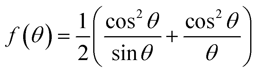
The XRD pattern, as exhibited in Fig. 1 is the obvious indication of the in situ formation of metallic platinum and its doping in PVDF films. The peaks appeared at 39.9°, 46.5°, 67.8° and 81.6° in PVF2Pt1.0 film corresponds to the diffraction from (111), (200), (220) and (311) lattice planes of fcc-Pt [Fm3m (225)] as per the JCPDS card no. 04-0802. Likewise, two intense diffraction peaks [i.e., (111) and (200)] are also present in PVF2Pt0.25 and PVF2Pt0.025 films as well. Nevertheless, the diffraction from (220) and (311) lattice planes are not appeared in these two films. It is also interesting to note that, especially in PVF2Pt1.0 film, the relative intensities of the (200) and (220) peaks are very close to the ‘bulk’, however, the relative intensity of (311) peak is considerably high (∼10%). In contrast, the relative intensities of (200) peak in PVF2Pt0.25 and PVF2Pt0.025 films are noticeably low. This result indicates that the PVF2Pt1.0 film is rich of {220} and {311} facets, rendering it of high interest for catalytic applications.8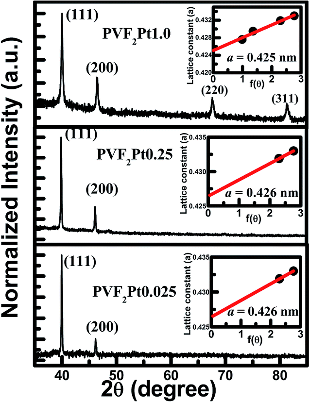 | ||
| Fig. 1 XRD pattern of Pt-NPs doped PVDF films where 2θ = 35 to 85° region is shown for indexing the diffraction peaks from Pt-NPs and inset figures show the Nelson–Riley plot of the respective films. | ||
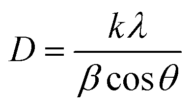
The XRD result also indicates that geometrical environment of PVDF may cause to change the electronic structure of Pt-NPs.23 The selective interaction of the counter part of PVDF (i.e., chain confirmation and crystallinity) with different crystal planes of Pt-NPs may also affect the growth rates and thus the diffraction alters the intensity of the different crystal planes of Pt-NPs. The average size of Pt-crystallites is calculated by using the Debye–Scherrer equation:
 | (1) |
 .
.
The photographs of the Pt-NPs doped PVDF films are quite transparent (Fig. 2a) and the transparency is reduced with the increasing density of Pt-NPs. This observation consistently matched with the transmittance spectra provided with the photograph of the films. The adequate flexibility of the Pt-NPs doped PVDF films is presented in Fig. 2b, where any undesirable micro cracks are not detectable. Furthermore, Pt-NPs doped PVDF films showing relatively larger absorbance in the UV region and a broad band appeared around 270 nm as depicted in Fig. 2c, indicates the absence of [PtCl6]2− ions and the full conversion of Pt–metallic (Pt0) states (ESI, Fig. S1†).24 The increasing trend of absorbance with concentration of Pt–salt indicates the increasing gradient of Pt-NPs formation. Therefore, the presences of Pt-NPs in PVDF films, as observed from XRD results are consistent with this observation. Besides this, the intense and a broad absorption features in the UV-region attributed to the strong d–sp interband transition comprising from Pt-NPs.14,25 As a consequence, the degree of UV-absorbance (ESI, Fig. S2†) undergoes a sharp improvement due to Pt-NPs doping as revealed in the inset of Fig. 2c.
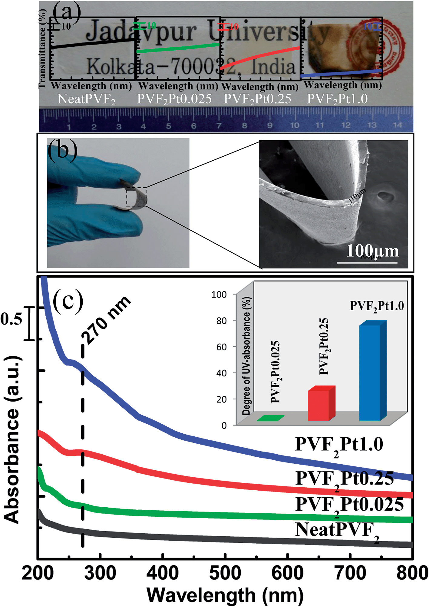 | ||
| Fig. 2 (a) Spectral transmittance (in visible region: 400–800 nm) and digital photograph of NeatPVF2 and Pt-NPs doped PVDF films, (b) superior flexibility of Pt-NPs doped PVDF (sample: PVF2Pt1.0) film is shown by digital photograph (left panel) and FE-SEM image (right panel), (c) UV-Vis absorbance spectra of NeatPVF2 and Pt-NPs doped PVDF films (for clarity, absorbance of each spectrum are shifted arbitrarily). The degree of UV-absorbance of Pt-NPs doped PVDF films is illustrated in the inset. | ||
The optical microscopic (OPM) images with cross-polarize view (inset images) of NeatPVF2 and Pt-NPs doped PVDF films are shown in Fig. 3(a–d). The images demonstrate that the small hump like structures over the surface of NeatPVF2 film (Fig. 3a) and these are atrophied tardily in Pt-NPs doped PVDF films (Fig. 3b–d). Interestingly, the directional fiber layers over PVDF surface are observed in PVF2Pt1.0 film (Fig. 3d) due to the influence of larger proportion of Pt-NPs in PVDF film (ESI, Fig. S3†). On the other hand polarized optical microscopic (POM) images (A⊥P) presented in the inset of Fig. 3(a–c) exhibit the presence of spherulitic feature that usually arises due to presence of linear optical anisotropy (birefringence effect) occur in α-phase and γ-phase orientations. The strong birefringent effect comprising from large spherulites (∼25 μm of average diameter) of compact and well-defined structure with Maltese-cross texture (shown by dotted lines in the inset of Fig. 3a) describe the predominant presence of α-crystalline phases in NeatPVF2 film.26 Commonly, these spherulitic growths are originated from the nucleus and their radial growths with clear boundaries are observed in NeatPVF2 film. These boundaries are due to the encroachment of spherulites. The OPM images of PVF2Pt0.025 and PVF2Pt0.25 films (inset of Fig. 3b and c) indicate the decreasing nature of large, strong α-spherulites and increasing tendency of relatively small, weekly birefringent spherulites which is the characteristic of γ-crystal (shown by dotted circles in inset of Fig. 3b). Thus the diminishing tendency of α-spherulites and subsequent appearance of γ-spherulites in Pt-NPs doped PVDF films imply that there may also exists β-spherulites which does not show optical anisotropy in polarizing optical microscopy images due to the weak birefringence nature.27 In contrast, PVF2Pt1.0 film does not represent any typical α- or γ-spherulites but the fibril like structure (obtained in unpolarized mode, Fig. 3d) shows the significant anomaly birefringent effect (depicted in the inset of Fig. 3d), probably due to the large difference of refractive index (optical anisotropy) comprising from the Pt and PVDF surfaces. The intense variation of the Pt–PVDF fibril structure probably hindered the view of typical γ-spherulitic structure in the surface of the film, if any.
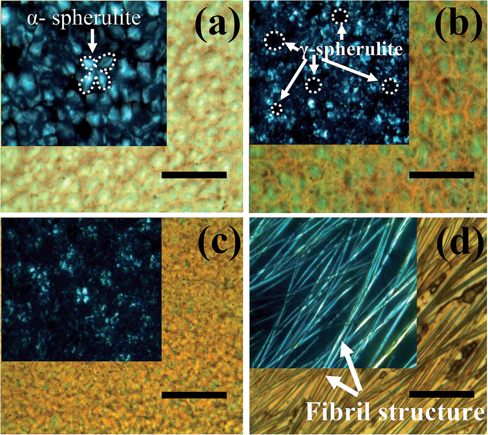 | ||
| Fig. 3 Optical microscopic images of (a) NeatPVF2, (b) PVF2Pt0.025, (c) PVF2Pt0.25, and (d) PVF2Pt1.0 films. The unpolarize (A║P) and cross polarize (A⊥P) (inset figures) views are shown in same scale bar: 50 μm. | ||
The detail surface morphology of NeatPVF2 and Pt-NPs doped PVDF films are examined through FE-SEM images depicted in Fig. 4(a–d). The typical fibril growth of α-spherulite (marked by arrow, Fig. 4a) is mainly observed on NeatPVF2 surface, whereas it remarkably diminishes in Pt-NPs doped PVDF films. In PVF2Pt0.025 film, a trace amount of α-spherulite (marked by dotted boundary, Fig. 4b) is appeared, however, it is completely diminishes in PVF2Pt0.25 and PVF2Pt1.0 films. Nevertheless, Pt-NPs are uniformly distributed over the surface of PVF2Pt0.025 film as shown through the enlarge view of the FE-SEM image (inset of Fig. 4b). In contrast, quite different surface morphologies are observed in PVF2Pt0.25 and PVF2Pt1.0 films, indicating the significant effect of in situ formation of Pt-NPs when concentration of Pt–salt increases. PVF2Pt0.25 film (Fig. 4c) exhibits the anisotropic distribution of Pt-nanoclusters (NCs) strips embedded within the PVDF surface (in Fig. 4c, few Pt-NCs strips are marked by arrows and a schematic diagram of one Pt-NCs strip has been cited). In addition, the presence of uniform Pt-NPs are also observed over the entire surface (in the inset of Fig. 4c) along with the random distribution of Pt-NCs strips. Furthermore, Pt-NCs strips are lengthy and quite well arranged (indicated by arrows in Fig. 4d) in PVF2Pt1.0 film, few well arranged Pt-NCs strips are marked with dotted lines. The enlarged view of the selected area in PVF2Pt1.0 film (demonstrate the inset of Fig. 4d) indicates that quite well disperse Pt-NPs are also present in between the region of Pt–NCs strips. The presence of Pt-NPs was further evidenced from energy dispersive X-ray spectroscopic (EDS) spectrum (ESI, Fig. S4†). The presence of C and F due to PVDF and Pt due to NPs formation were well detected in the EDS spectrum. Thus it is self-evident that the surface morphology can be tuned by simply changing the concentration of the Pt–salt. As this large variation of the surface morphology is solely depend on the size, shape, and distribution of Pt-NPs over PVDF surface, so it indicates that Pt-NPs doped PVDF films may have versatile functionalities for chemical sensor applications.28
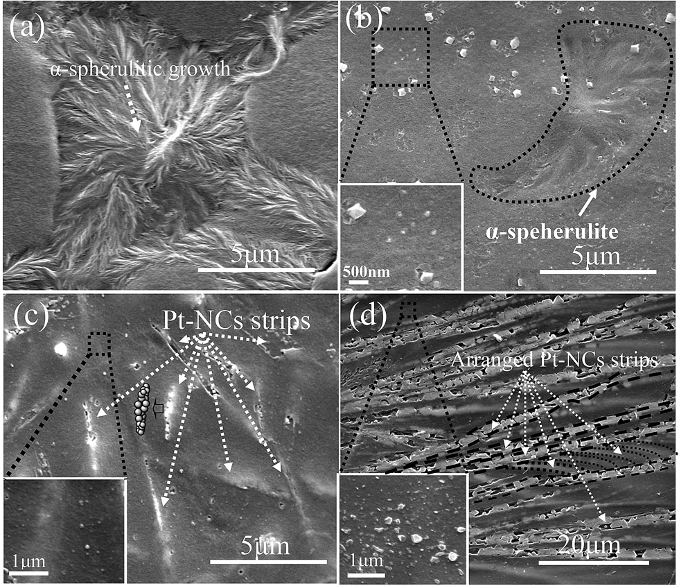 | ||
| Fig. 4 FE-SEM images of (a) NeatPVF2, (b) PVF2Pt0.025, (c) PVF2Pt0.25, and (d) PVF2Pt1.0 films. In inset, the enlarge view of the selected region of the respective images are shown. | ||
The FT-IR spectra of NeatPVF2 as well as Pt-NPs doped PVDF films are shown in Fig. 5a and corresponding vibrational bands are labeled as per the presence of crystalline phases. It exhibits NeatPVF2 film predominantly composed of α-crystalline phase attributing from the strong absorption peaks at 1211, 1150, 976, 856, 796, 764, 613 and 532 cm−1.29 In contrast, Pt-NPs doped PVDF films illustrate two additional intense peaks arise at 1277 and 1234 cm−1 are due to the nucleation of the β and γ-phases respectively.4,9,29 Few α-characteristic vibrational bands at 976, 796, 764, 532 cm−1 are still appeared in PVF2Pt0.025 film, indicates 0.025 wt% of Pt–salt is not sufficient to hinder the α-crystalline growth completely. Nevertheless, the improvement of the intensity of 841 cm−1 and clear appearance of 1277 as well as 1234 cm−1 bands indicate that the nucleation of the electroactive β and γ-phases takes place even with the trace amount of Pt-NPs prepared from 0.025 wt% (0.048 mM) of Pt–salt. Furthermore, PVF2Pt0.25 film exhibits the complete removal of the non-polar α-characteristic phase and complete conversion of the electroactive counterpart of PVDF. Some occurrences are observantly kept in view that if we increase the concentration of Pt–salt gradually in PVDF matrix, then further improvement of the β and γ-band intensity has also been notified (ESI, Fig. S5†). It is mentionable that for the qualitative analysis of the α, β and γ-phases the absorbance is normalized at 1072 cm−1 band as it has a linear dependence with the film thickness regardless of crystalline modification.5 The absorption intensity ratio of β (I1277) and α (I764)-phases, i.e., I1277/I764 in NeatPVF2 and Pt-NPs doped PVDF films is depicted in Fig. 5b, reveals that it gradually increases as the concentration of Pt–salt (i.e., also Pt-NPs) increases and reached maximum (i.e., I1277/I764 = 0.93) in PVF2Pt1.0 film. It is interestingly noticeable that even though the PVF2Pt0.25 film does not exhibit the α-characteristic bands (Fig. 5a), however I1277/I764 is far below from its maximum, observed in PVF2Pt1.0 film. This is significantly pointed out that PVF2Pt0.25 film has large amount of additional contribution other than the β-phase, i.e., the γ-phase, as evident from the relatively intense 1234 cm−1 band (Fig. 5a). It is noteworthy to mention that as NeatPVF2 film predominately consists of α-phase, therefore for comparison, the contribution from the β and γ-phases of NeatPVF2 film is not taking into account for further analysis. The absorption intensity ratio of β (I1277) and γ (I1234)-phases i.e., I1277/I1234 is also demonstrated in Fig. 5b, indicates the hindering of γ-crystalline growth when the concentration of Pt-NPs is increased gradually. Thus it seems that PVF2Pt0.25 and PVF2Pt1.0 films contain a large proportion of the β-phase.
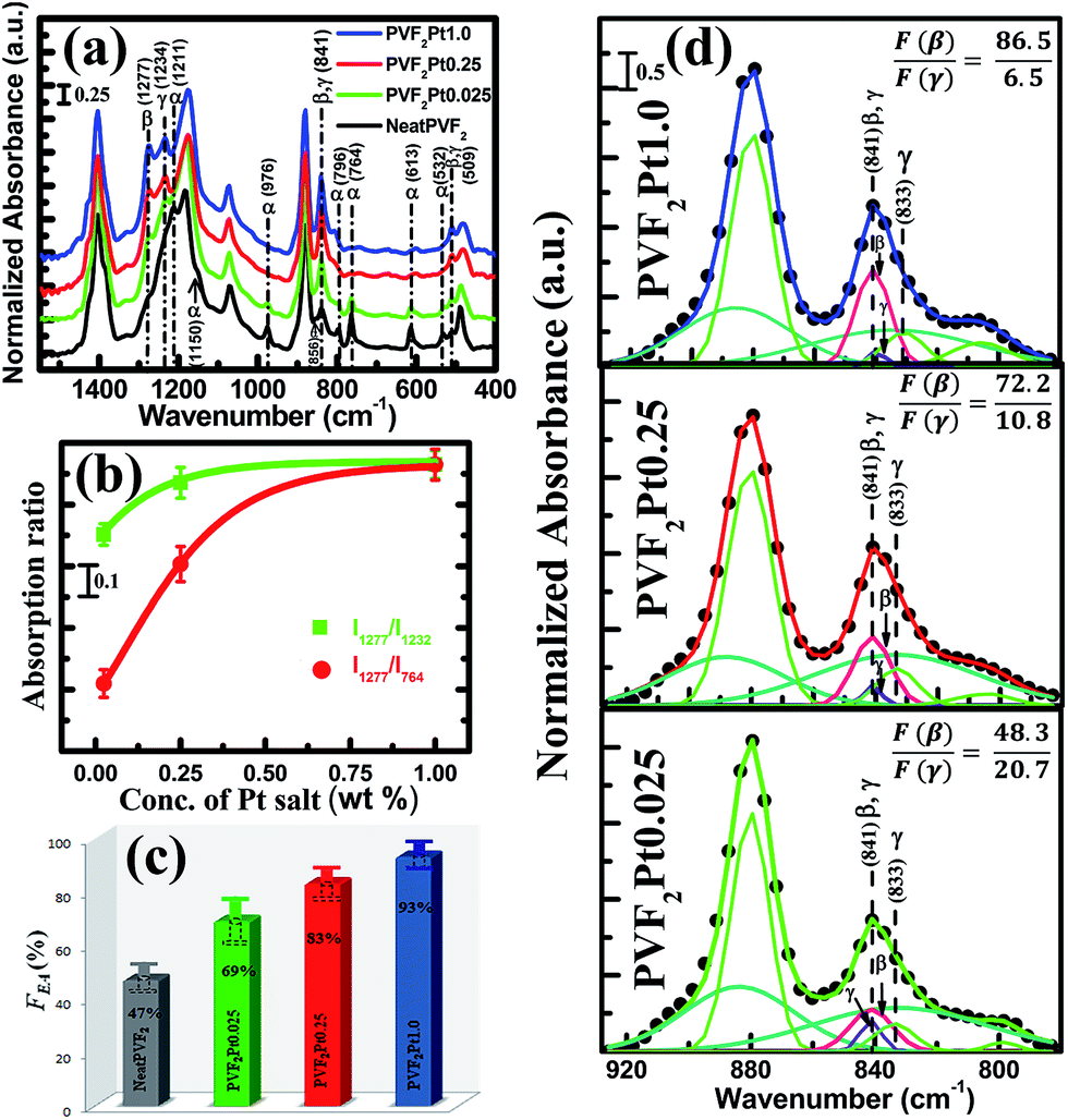 | ||
| Fig. 5 (a) FT-IR spectra of NeatPVF2 and Pt-NPs doped PVDF films in 1550–400 cm−1 frequency region, (b) dependence of the absorption ratio of β and α-phases (I1277/I764) as well as β and γ-phases (I1277/I1234) of Pt-NPs doped PVDF films with concentration of Pt–salt from FT-IR spectra are shown, (c) the percentage of FEA for NeatPVF2 and Pt-NPs doped PVDF films, (d) the deconvolution of the FT-IR spectra (920–780 cm−1) of Pt NPs doped PVDF films is shown. The dotted points are experimental data and the solid from the best curve fit. The ratio of F(β) and F(γ) are mentioned in the inset. | ||
It is to be mentioned that the 841 cm−1 band strongly appeared in Pt-NPs doped PVDF films (Fig. 5a), is common characteristic of electroactive β and γ-phases.4,9,29,30 Thus the absorption intensity at 841 cm−1 band can be assigned to quantify the relative proportion of electroactive phases (i.e., FEA) attributing to both β and γ-phases. The FEA is related with the eqn (2) as follows,
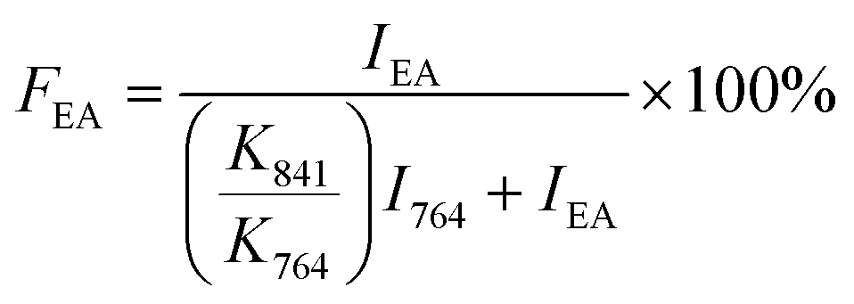 | (2) |
One important consequence of eqn (2) has been noted, as the rapid growth of electroactive phase (FEA) formation with increasing amount of Pt-precursor (Fig. 5c) up to 1.0 wt% of Pt–salt concentration has been occurred and then slowly improved up to 99% of FEA (ESI, Fig. S6†). The quantification of individual β and γ-phases is also performed by curve deconvolution of 841 cm−1 band (shown in Fig. 5d), where the broadening contribution due to γ-phase and sharp well resolved peak for β-phase has been considered.30 The equations of (3a) and (3b) are used to quantify the relative proportion of electroactive β and γ-phases individually.
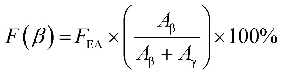 | (3a) |
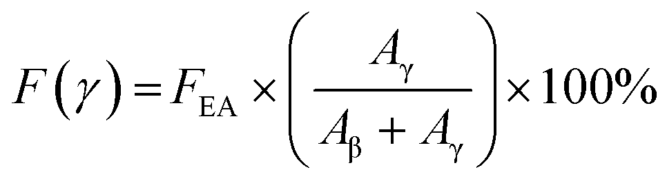 | (3b) |
These results emphasize on the fact that Pt-NPs play a significant catalytic role for nucleating the piezoelectric β-phase and subsequent stabilization. This can be interpreted by the surface charge (of NPs) and dipoles (of PVDF) interaction model as thought previously.4 A clear frequency shifting of the CH2 asymmetric (νas) and symmetric (νs) stretching vibrational modes are observed (Fig. 6a) in Pt-NPs doped PVDF films in comparison with NeatPVF2 film, is the indication of the interfacial interaction causes from the surface charge of the Pt-NPs (σeff+) and CH2 (also CF2) dipoles (δeff−) of PVDF.
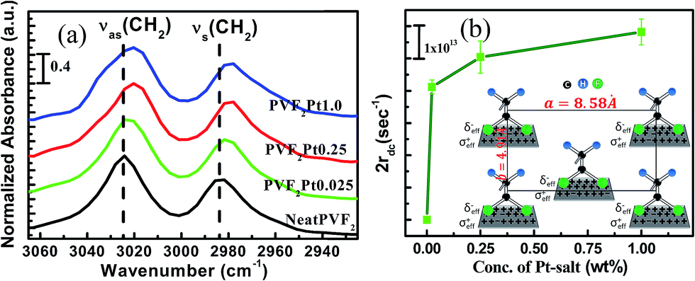 | ||
| Fig. 6 (a) FT-IR spectra of NeatPVF2 and Pt-NPs doped PVDF films in 3060–2940 cm−1 region; (b) Variation of damping coefficient (2rdc) as function of concentration of Pt–salt. The inset shows the unit cell of β-phase, where the interfacial interaction between the surface charge of Pt-NPs (assuming the effective positive surface charge density of nano-particles i.e. σeff+) and CF2 dipoles (δeff−) are illustrated. | ||
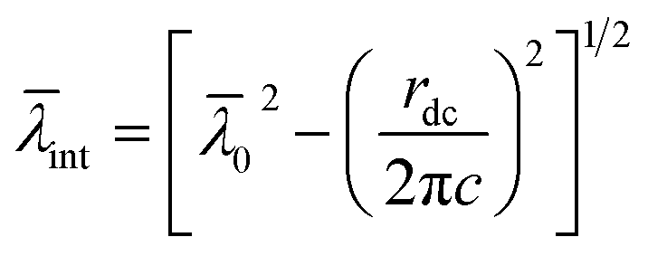
Recently, for clarifying this type of interfacial interaction, a damping constant (2rdc) associated with the frequency of CH2 vibration (ν-CH2) is proposed by considering the frequency shift from the NeatPVF2 film.33 It has been assumed that the effective mass of CH2 dipoles is increased due to the interfacial interaction. As a result a damping may occur; this decreases the vibrational frequency (i.e., wavenumber) of the CH2 stretching vibration. The damping constant (2rdc) is related to the wavenumber (![[small lambda, Greek, macron]](https://www.rsc.org/images/entities/i_char_e0cc.gif) int) of CH2 stretching vibration (ν-CH2) due to damped oscillation for Pt-NPs doped PVDF films as,
int) of CH2 stretching vibration (ν-CH2) due to damped oscillation for Pt-NPs doped PVDF films as,
 | (4) |
0 is the wavenumber of ν-CH2 in damping free vibration, occur in NeatPVF2 film and int are the corresponding wavenumber due to damped vibration possess Pt-NPs doped PVDF films; c is the velocity of the light. Fig. 6b shows that damping constant 2rdc increases asymptotically as a function of Pt-NPs loading in PVDF matrix. Thus the increase of 2rdc value indicates the improvement of interfacial interaction which improves β-phase content. The inset of Fig. 6b represents a unit cell of β-phase, where the interfacial interaction is represented.
Crystallinity of the NeatPVF2 and Pt-NPs doped PVDF films are evaluated from the XRD pattern by curve deconvolution technique, demonstrated in Fig. 7. NeatPVF2 film exhibits the diffraction peaks at 17.6° (100), 18.2° (202), 19.7° (110), 26.2° (021) and a shoulder at 25.4° (120) are the characteristic of α-crystalline phase.11,27 Thus NeatPVF2 film consists of predominantly α-crystalline phase which is consistent with FT-IR spectra as shown in Fig. 5a. Apparently, PVF2Pt0.025 film shows the α-phase attributing from 17.6° (100) and 18.5° (202) diffraction peaks. Moreover, the diffraction peak at 18.5° (202) in Pt-NPs doped PVDF films is attributing the presence of the γ-phase as the α-characteristic peak at 17.6° is absent. Likewise, the main intense diffraction peak at 20.5° is the dual signature of the β and γ phases27 that needs curve deconvolution to resolve the individual contribution. Applying deconvolution method, the presence of β-phase at 20.8° (110/220) and γ-phase at 20.2° (110) are classified individually.
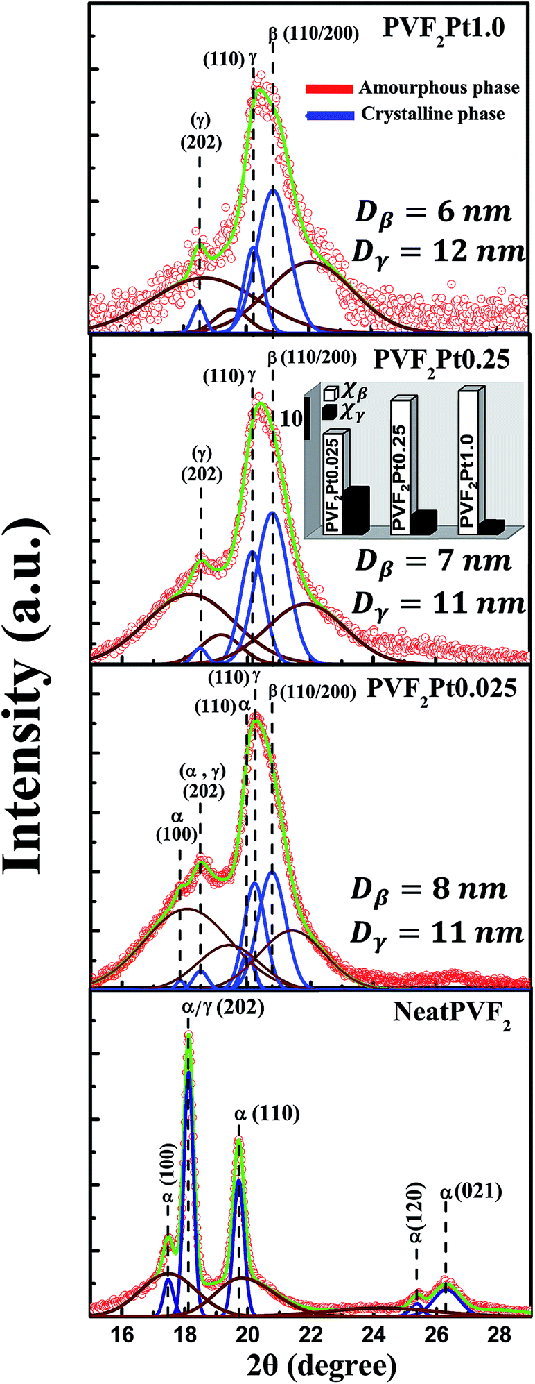 | ||
| Fig. 7 The curve deconvolution of XRD pattern in 16–28° (2θ) range of NeatPVF2 and Pt-NPs doped PVDF films. The degree of β and γ-crystallinity is depicted within the inset figure and corresponding crystallite size (Dβ and Dγ) is also mentioned. | ||
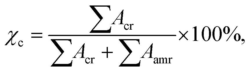
The degree of crystallinity (χc) is calculated from
 | (5) |
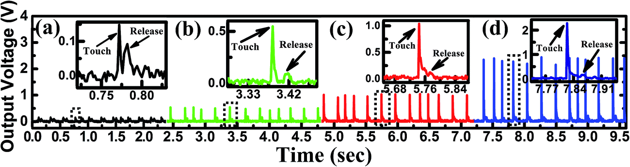 | ||
| Fig. 8 Finger touch response (rectified output voltage) from (a) NeatPVF2, (b) PVF2Pt0.025, (c) PVF2Pt0.25 and (d) PVF2Pt1.0 films at room temperature. The insets show the enlarge view of one selected peak responsible for press and release of gentle finger touch (ESI, Fig. S11 and ESI Video S1†). | ||
Therefore, the output voltages of these films (ESI, Fig. S11†) are not as symmetrical as typically found in normal piezo-electric nanogenerators (NGs).33 Furthermore, the high output voltage generation and tremendous touch sensitivity (ESI, Video S1†) from unpoled Pt-NPs doped PVDF films signifying the great potential feasibility to develop energy harvester which is expected to be a future power source for next generation portable electronic devices.37 Furthermore, upon electrical poling, it is also expected that high piezoelectric β-phase containing Pt-NPs doped PVDF films will exhibit considerably high piezoelectric output, probably ideal for flexible nanogenerator fabrication or self-charging battery separator.38
The room temperature PL spectra illustrated in Fig. 9A, exhibit the intense broad UV-emissions from UV-B to UV-A regions in Pt-NPs doped PVDF films. It attributes to the fact that Pt-NPs act as an important role for generating UV-emission as there is a forbidden emission in NeatPVF2 film (ESI, Fig. S12†). Deconvolution of the PL-spectrum indicates that each of the emission spectra is composed of mainly three Gaussian curves, viz. B, A1 and A2 curves (mentioned in Fig. 9A). The A1 and A2 curves belong to UV-A region, whereas curve B belongs to UV-B region. The resultant contribution of B and A2 curves, revealed from their integrated areas, is more pronounced than that of the A1 curve with the lower concentration of Pt-NPs doped in PVDF matrix. The overall broad emission indicates that the Pt-NPs doped PVDF films have good luminescence quality. It is also observed that UV-emission peaks are shifted towards the lower wavelength with increasing concentration of Pt-NPs (ESI, Fig. S13†). This might be due to the formation of Pt–NCs, observed in PVF2Pt0.25 and PVF2Pt1.0 films (Fig. 4c and d).39,40 It has been found that the frequency of the Localized Surface Plasmon Resonance (LSPR) can be tuned by changing the size, shape, and dielectric constant of the surrounding medium for a given metal-dielectric combination.41 Theoretically, it has been established that noble metals give rise the PL due to the direct recombination of the conduction-band electrons near the Fermi level with the holes in the d-band.42 Thus, the entire photo excitation and emission can be explained by the schematic illustrated in Fig. 9B. Initially, the d-band electrons lead to interband transitions by absorbing the incident photons [Fig. 9B(i)]. The energy required to promote these electrons from the filled d-band to the unoccupied sp-conduction band above the Fermi level is supplied by the photon energy (hν). Both the electrons and holes can relax by scattering with phonons then recombine radiatively to produce the emission. But this interband transition only involved the visible emission from metal NPs42 which is forbidden in Pt-NPs doped PVDF film. It should also be noted that to data very few reports are available where intense visible luminescence is observed for Pt-NPs.17,43 In contrast, UV-emission from the Pt-NPs is not reported yet.
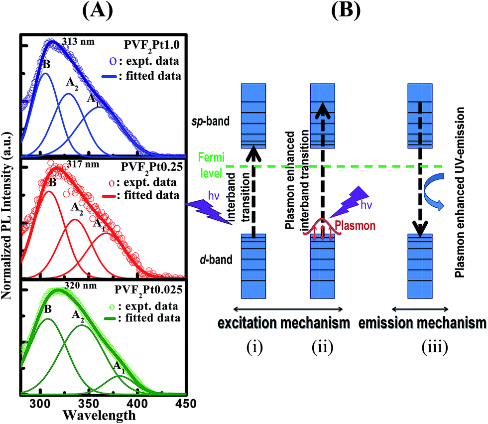 | ||
| Fig. 9 (A) The room temperature normalized PL spectrum of Pt-NPs doped PVDF films. (B) A schematic diagram of excitation and emission mechanism [(i) excitation due to only interband transition and (ii) due to plasmon enhanced interband transition, (iii) due to plasmon enhanced UV-emission] to represent the UV-photoemission from Pt-NPs doped PVDF films. | ||
This UV-emission is probably due to the coupling effect between LSPR and d–sp interband transition.39 The enhancement of interband transition followed by the plasmons coupling (shown by the schematic diagram of Fig. 9B(ii) and (iii)) of electronic transitions responsible for intense UV-emission. It should also be noted that the frequency of the LSPR of platinum is located in the ultraviolet region43,44 and likewise we have also observed the strong d–sp interband transition of Pt-NPs as evident from UV-Vis absorption spectra (shown in Fig. 2c). Thus, under the UV-light excitation (shown in Fig. 9B(ii)) both d–sp interband transition of single electron and surface plasmon absorption also may occur, as a consequence, coupling between LSPR and interband transition gives rise plasmon enhanced UV-emission (as shown in schematic of Fig. 9B(iii)). Thus Pt-NPs doped PVDF film promises a new type of photonic application apart from its electroactive activity, extends its importance as potential multifunction film for versatile sensor fabrication.
Conclusions
The multifunctional Pt-NPs doped PVDF films are prepared using a simple solvent casting technique. By simply controlling the platinum precursor amount, almost complete conversion (99%) to electroactive phases is achieved as evident from spectroscopic and crystallographic information. In other words, we have proposed a simple method of in situ Pt-NPs synthesis that might have enormous advantage over a typical catalysis. In contrast to a typical catalysis, a new type of catalytic role in crystalline phase conversion in PVDF, i.e., from non-polar α-phase to electroactive β and γ-phases is noticed. The overall crystallinity (χc) is reduced upon Pt-NPs doping and more importantly, piezoelectric β-crystallinity (χβ) is considerably improved. This signifies high dielectric strength and can be used to build multilayer capacitors for energy storage. Furthermore, higher yield of β-crystallinity in Pt-NPs doped film promotes considerable higher (4 times) remnant polarization in comparison to the neat PVDF film, indicating an improved ferroelectric properties for non-volatile memory. In this work, we have also shown that tactile sensors made with un-poled Pt-NPs doped PVDF films exhibiting ultra-sensitive human finger touch response, possibly eliminating the traditional electrical poling steps. A considerable enhancement (∼16 times) of rectified output voltage is realized upon Pt-NPs doping in PVDF. Potentially, these tactile sensors could be used to harvest energy and power small portable and wearable electronic devices. The PL-properties of Pt-NPs doped PVDF film aid an additional new avenue in photonic to be utilized as a flexible UV-emitter.Conflict of interest
The authors declare no competing financial interest.Acknowledgements
Authors are grateful to DST, Govt. of India for developing instrumental facilities under FIST-II programme and providing the INSPIRE fellowship (IF130865) to Mr Sujoy Kumar Ghosh. We are also thankful to Mr Samiran Garain for his skillful FE-SEM operation and Mr Biswajit Mahanty for demonstrating the way of optimized electrical signal recording.References
- Z. L. Wang, J. Phys. Chem. Lett., 2010, 1, 1388–1393 CrossRef CAS.
- A. J. Lovinger, Science, 1983, 220, 1115–1121 CAS.
- K. Müller, D. Mandal, K. Henkel, I. Paloumpa and D. Schmeisser, Appl. Phys. Lett., 2008, 93, 112901 CrossRef PubMed.
- D. Mandal, K. J. Kim and J. S. Lee, Langmuir, 2012, 28, 10310–10317 CrossRef CAS PubMed.
- P. Martins, A. C. Lopes and S. Lanceros-Mendeza, Prog. Polym. Sci., 2014, 39, 683–706 CrossRef CAS PubMed.
- W. Li, Q. Meng, Y. Zheng, Z. Zhang, W. Xia and Z. Xu, Appl. Phys. Lett., 2010, 96, 192905 CrossRef PubMed.
- M. Segev-Bar and H. Haick, ACS Nano, 2013, 7, 8366–8378 CrossRef CAS PubMed.
- S. Mourdikoudis, M. Chirea, T. Altantzis, I. Pastoriza-Santos, J. Pérez-Juste, F. Silva, S. Balsc and L. M. Liz-Marzán, Nanoscale, 2013, 5, 4776–4784 RSC.
- D. Mandal, K. Henkel and D. Schmeißer, Mater. Lett., 2012, 73, 123–125 CrossRef CAS PubMed.
- C. Xu, K. J. Kim, Y. Wang, S. Yoon, G. Ren, D. Mandal, and B. Li, In Flexible Nanogenerator and Nano-Pressure Sensor Based on Nanofiber Web of PVDF and its Copolymers, in Soft Fibrillar Materials: Fabrication and Applications, ed. X. Y. Liu and J.-L. Li, Wiley-VCH, Weinheim, Germany, 2013, pp.233–264 Search PubMed.
- P. Zhang, X. Zhao, X. Zhang, Y. Lai, X. Wang, J. Li, G. Wei and Z. Su, ACS Appl. Mater. Interfaces, 2014, 6, 7563–7571 CAS.
- M. Ahmad and J. Zhu, J. Mater. Chem., 2011, 21, 599–614 RSC.
- O. D. Jayakumar, N. Manoj, V. Sudarsan, C. G. S. Pillai and A. K. Tyagi, CrystEngComm, 2011, 13, 2187–2190 RSC.
- W. Kaifeng, Z. Haiming, L. Zheng, R. William and L. Tianquan, J. Am. Chem. Soc., 2012, 134, 10337–10340 CrossRef PubMed.
- N. Mazumder, D. Sen, S. Saha, U. K. Ghorai, N. S. Das and K. K. Chattopadhyay, J. Phys. Chem. C, 2013, 117, 6454–6461 CAS.
- J. B. You, X. W. Zhang, J. J. Dong, X. M. Song, Z. G. Yin, N. F. Chen and H. Yan, Nanoscale Res. Lett., 2009, 4, 1121–1125 CrossRef CAS PubMed.
- C. Y. Kang, C. H. Chao, S. C. Shiu, L. J. Chou, M. T. Chang, G. R. Lin and C. F. Lin, J. Appl. Phys., 2007, 102, 073508–073515 CrossRef PubMed.
- V. Sencadas, P. Martins, A. Pitães, M. Benelmekki, J. Ribelles and S. Lanceros-Mendez, Langmuir, 2011, 27, 7241–7249 CrossRef CAS PubMed.
- L. Li, M. Zhang, M. Rong and W. Ruan, RSC Adv., 2014, 4, 3938–3943 RSC.
- V. K. Tiwari, D. K. Avasthi and P. Maiti, ACS Appl. Mater. Interfaces, 2011, 3, 1398–1401 CAS.
- H. J. Ye, L. Yang, W. Z. Shao, Y. Li, S. B. Sun and L. Zhen, RSC Adv., 2014, 4, 13525–13532 RSC.
- P. Zapata, D. Mountz and J. C. Meredith, Macromolecules, 2010, 43, 7625–7636 CrossRef CAS.
- Z. Kónya, V. F. Puntes, I. Kiricsi, J. Zhu, P. Alivisatos and G. A. Somorjai, Catal. Lett., 2002, 81, 137–140 CrossRef.
- N. Viet-Long, O. Michitaka, N. N. Van, C. Minh-Thi and N. Masayuki, Adv. Nat. Sci.: Nanosci. Nanotechnol., 2012, 3, 025005–025008 CrossRef.
- R. C. Johnson, J. Li, J. T. Hupp and G. C. Schatz, Chem. Phys. Lett., 2002, 356, 534–540 CrossRef CAS.
- R. Gregorio Jr and C. Marcelo, J. Polym. Sci., Part B: Polym. Phys., 1994, 32, 859–870 CrossRef PubMed.
- B. S. Ince-Gunduz, R. Alpern, D. Amare, J. Crawford, B. Dolan, S. Jones, R. Kobylarz, M. Reveley and P. Cebe, Polymer, 2010, 51, 1485–1493 CrossRef CAS PubMed.
- Y. Kang, M. Li, Y. Cai, M. Cargnello, R. E. Diaz, T. R. Gordon, N. L. Wieder, R. R. Adzic, R. J. Gorte, E. A. Stach and C. B. Murray, J. Am. Chem. Soc., 2013, 135, 2741–2747 CrossRef CAS PubMed.
- D. Mandal, K. Henkel and D. Schmeisser, J. Phys. Chem. B, 2011, 115, 10567–10569 CrossRef CAS PubMed.
- R. Gregorio Jr and D. S. Borges, Polymer, 2008, 49, 4009–4016 CrossRef PubMed.
- C. R. Bowen, H. A. Kim, P. M. Weaver and S. Dunn, Energy Environ. Sci., 2014, 7, 25–44 CAS.
- D. Lingam, A. R. Parikh, J. Huang, A. Jain and M. Minary-Jolandan, Int. J. Smart Nano Mater., 2013, 4, 229–245 CrossRef.
- D. Mandal, K. Henkel and D. Schmeißer, Phys. Chem. Chem. Phys., 2014, 16, 10403–10407 RSC.
- M. Y. F. Elzayat, S. El-Sayed, H. M. Osman and M. Amin, Polym. Eng. Sci., 2012, 52, 1945–1950 CAS.
- F. Guan, J. Wang, J. Pan, Q. Wang and L. Zhu, Macromolecules, 2010, 43, 6739–6748 CrossRef CAS.
- W. Heywang, K. Lubitz and W. Wersing, Piezoelectricity: Evolution and Future of a Technology, ed. R. Hull Jr, R. M. Osgood, J. Parisi and H. Warlimont, Springer Series in Materials Science, 2008, pp. 157–176, ISBN 978-3-540-68680-4 Search PubMed.
- Z. Li, X. Zhang and G. Li, Phys. Chem. Chem. Phys., 2014, 16, 5475–5479 RSC.
- X. Xue, S. Wang, W. Guo, Y. Zhang and Z. L. Wang, Nano Lett., 2012, 12, 5048–5054 CrossRef CAS PubMed.
- J. Zheng, C. Zhou, M. Yu and J. Liu, Nanoscale, 2012, 4, 4073–4083 RSC.
- H. Kawasaki, H. Yamamoto, H. Fujimori, R. Arakawa, M. Inada and Y. Iwasaki, Chem. Commun., 2010, 46, 3759–3761 RSC.
- S. Link and M. A. El-Sayed, Annu. Rev. Phys. Chem., 2003, 54, 331–366 CrossRef CAS PubMed.
- A. Mooradian, Phys. Rev. Lett., 1969, 22, 185–187 CrossRef CAS.
- H.-T. Sun and Y. Sakka, Sci. Technol. Adv. Mater., 2014, 15, 014205–014218 CrossRef.
- C. Langhammer, Z. Yuan, I. Zorić and B. Kasemo, Nano Lett., 2006, 6, 833–838 CrossRef CAS PubMed.
Footnote |
| † Electronic supplementary information (ESI) available. See DOI: 10.1039/c4ra06334a |
| This journal is © The Royal Society of Chemistry 2014 |