
Hierarchical silicon nanostructured arrays via metal-assisted chemical etching†
Hao Lin‡
a,
Ming Fang‡a,
Ho-Yuen Cheungb,
Fei Xiuad,
SenPo Yipad,
Chun-Yuen Wongb and
Johnny C. Ho*acd
aDepartment of Physics and Materials Science, City University of Hong Kong, 83 Tat Chee Avenue, Kowloon Tong, Kowloon, Hong Kong. E-mail: johnnyho@cityu.edu.hk
bDepartment of Biology and Chemistry, City University of Hong Kong, 83 Tat Chee Avenue, Kowloon Tong, Kowloon, Hong Kong
cCentre for Functional Photonics (CFP), City University of Hong Kong, 83 Tat Chee Avenue, Kowloon Tong, Kowloon, Hong Kong
dShenzhen Research Institute, City University of Hong Kong, Shenzhen, China
First published on 19th September 2014
Abstract
Hierarchically arranged nanostructures, configured in both nanopillars and nanoholes, have been fabricated via a low-cost approach that combines metal-assisted chemical etching (MaCE), nanosphere lithography and conventional photolithography. By manipulating the catalyst morphology as well as the deposition method, different interesting nanostructures like nanowalls and nanograsses were fabricated at the galleries among the nanopillar blocks. Using a similar strategy, hierarchical negative structures (nanoholes) have also been successfully demonstrated. The successful construction of these diversified hierarchical nanostructures illustrates that MaCE could be employed as a feasible, low-cost method for multi-scale silicon micro/nano machining, which is highly desirable for widespread applications, including tissue engineering, optoelectronics, photonic devices and lab-on-chip systems.
Introduction
Hierarchical micro/nano structures possess the unique interfacial properties of wetting, adhesion, thermal management, electrical conduction and light trapping, in which these properties can work synergistically and offer superior material/device performances. These structures are of great interest for widespread applications such as optoelectronics,1,2 photonic devices,3–6 bio-/chemical-sensors,7–9 and biomedicine.10,11 Usually, these structures could be fabricated by employing electron-beam lithography (EBL), focused-ion-beam lithography (FIB) and reactive-ion etching (RIE) for patterning and/or etching. However, these techniques are only suitable for small-area fabrications owing to their high cost and low throughput, which have severely retarded the practical applications of these hierarchical materials. In recent years, wet chemical etching methods, such as electrochemical micromachining (ECM)12,13 and metal-assisted chemical etching (MaCE), have also been actively explored for the fabrication of high-aspect-ratio silicon-based nanostructures.14–16 Compared with the standard dry etching methods, wet etching techniques hold several key advantages, including the low fabrication cost, elimination of surface damages and more importantly, achievable high structural aspect ratios. For instance, a recent report by Chang and Sakdinawat showed that high-resolution Si nanostructures (e.g., nanowalls with a 32 nm width, 136 nm period and 2.5 μm height) could be formed by MaCE for applications in hard X-ray diffractive optics.17 Moreover, by combining MaCE with the low-cost nanosphere lithography, highly ordered silicon nanopillar, nanopencil and nanocone arrays have been successfully fabricated in a controllable manner.18,19 Nevertheless, although MaCE has been successfully employed for the fabrication of uniformly distributed Si nanostructures, it is still rarely utilized to obtain hierarchical micro/nano structures.Here, we report the fabrication of hierarchically arranged nanostructures, in the configuration of both pillars and holes, by MaCE coupled with polystyrene (PS) nanosphere lithography as well as conventional photolithography. By manipulating the catalyst deposition methods and etching conditions, we can attain diversified hierarchical micro/nano structures, which demonstrate that MaCE could be employed as a feasible and low-cost method to achieve various large-area hierarchical micro/nano structures for technological utilization.
Experimental
Single-crystalline p-type (100) Si wafers were used for the fabrication of the hierarchical silicon micro/nano structures. Metal films were deposited through electron-beam evaporation at a rate of 1–2 Å s−1. Photolithography was carried out in a class 100 cleanroom, employing a MA/BA6 mask aligner (Karl Suss) and AZ 5214E photoresist (Micro-Chemicals). Monodispersed PS nanospheres were purchased from Microparticles GmbH. Closely packed PS nanosphere monolayers were obtained by assembling the spheres on the surface of water through the Langmuir–Blodgett (LB) method, and then transferred on to the target wafers. The assembled nanospheres were shrunk by oxygen plasma etching and used as the deposition or etching masks for subsequent metal patterning. To conduct MaCE, the silicon wafers with a patterned catalyst were immersed in HF–H2O2 (4.8 M, 0.2 M) aqueous solutions at room temperature for 20–60 min in the dark. After etching, the Au catalyst was removed using an aqua regia solution (HNO3–HCl, 1![[thin space (1/6-em)]](https://www.rsc.org/images/entities/char_2009.gif) :3 in volume).
:3 in volume).
Results and discussion
The MaCE of silicon typically takes place in a system that contains silicon wafers, metal catalysts (Ag, Au, or Pt) and an etchant solution (HF and H2O2 mixtures). The etching process in principle is chemical reduction/oxidation reactions occurring at the metal–Si interface.14,16 The oxidants, such as H2O2, are reduced to water by taking electrons from the metal catalyst, leaving holes in the metal. The holes are further injected into the silicon and cause the oxidization of the interfacial silicon. The oxidized silicon is then dissolved by HF, leading to the forward movement of the metal catalyst, and thus the catalyzed etching takes place continuously. Because of this above-mentioned etching mechanism, the cross-sectional shape of the etched structures is basically determined by the pattern of the metal catalyst. Therefore, employing a metal nanomesh and nanodisk as the catalyst, various silicon nanostructures, including nanopillars and nanoholes, could be obtained (ESI, Fig. S1†). As the etching reaction mainly occurs at the metal–silicon interface, high-aspect ratio nanostructures could be obtained accordingly with the proper control of the etching conditions.In order to obtain hierarchical or patterned nanopillar arrays, we first fabricated patterned metal nanomeshes on a silicon surface by combining nanosphere lithography and conventional photolithography. It is known that Ag and Au are the most commonly used catalysts in MaCE. In this work, we decided to select Au as the catalyst, since it has been demonstrated to have better film stability than Ag in the etching solution, in which this stability is highly crucial to achieve a smooth etched surface.20–22 In general, we can obtain Au mesh patterns through three different deposition methods by changing the sequence of the two lithographic processes, namely, type I, type II and type III, as illustrated in Fig. 1a–c (see ESI, Fig. S2† for details). After the catalyst deposition, the silicon chips were then submerged in a HF–H2O2 solution to undergo MaCE. During the process, the silicon underneath the metal film (catalyst) was etched, leaving the uncovered regions as nanopillars after the etching process (Fig. 1d).
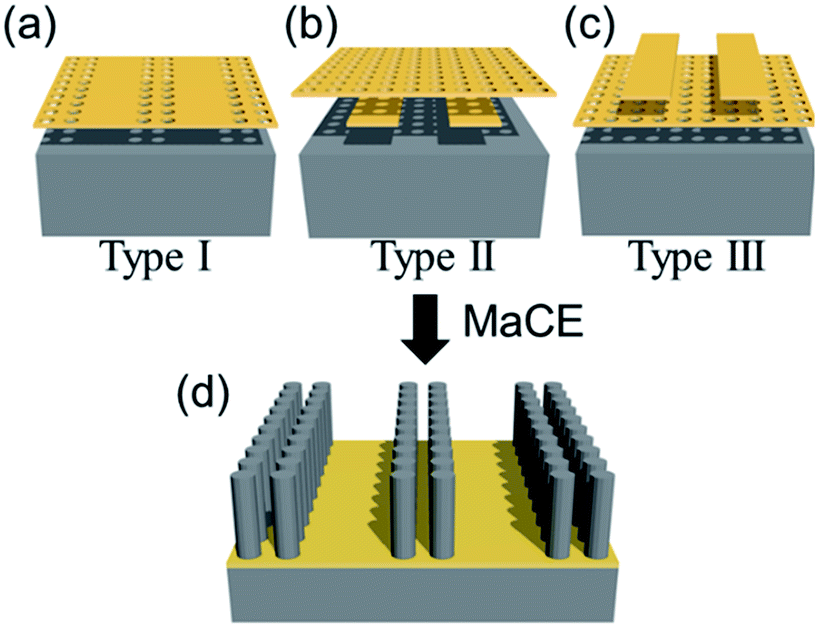 | ||
| Fig. 1 Schematic illustration for the fabrication of patterned nanopillar arrays via metal-assisted wet etching. (a–c) Gold nanomeshes (catalyst) fabricated with three different patterning methods and (d) obtained hierarchical nanostructures after the MaCE process. | ||
In predictions, the patterned regions (continuous metal films) should generate structures with smooth side walls and flat backgrounds after etching. However, our experimental results reveal that the three catalyst patterns with a different deposition sequence (i.e. type I, II or III) could give significantly distinct morphologies, and none of them led to a flat background (Fig. 2). Specifically, when using the type I Au catalyst film (Fig. 1a), a ridge was formed under the continuous metal film (Fig. 2a). It is obvious that the reaction rate at the center region (without any pattern) was much lower than that at the edge region (with patterns), which caused this non-flat etching background. In the second case, where type II Au patterns (Fig. 1b) were used as the catalyst, the morphology obtained was very close to our expectation; in any case, a closer look confirms that there are continuous silicon walls at the edges of the micropatterns, and simultaneously, the etching depth of the patterned regions was slightly smaller than that of the meshed regions (Fig. 2b). Finally, when type III Au catalyst patterns were used, very thin grass-like nanostructures appeared among the regular pillar arrays (Fig. 2c), which is somewhat different to the morphologies obtained in the first two cases. At the same time, it is noted that there is no noticeable difference in the etching depth observed over the different regions here.
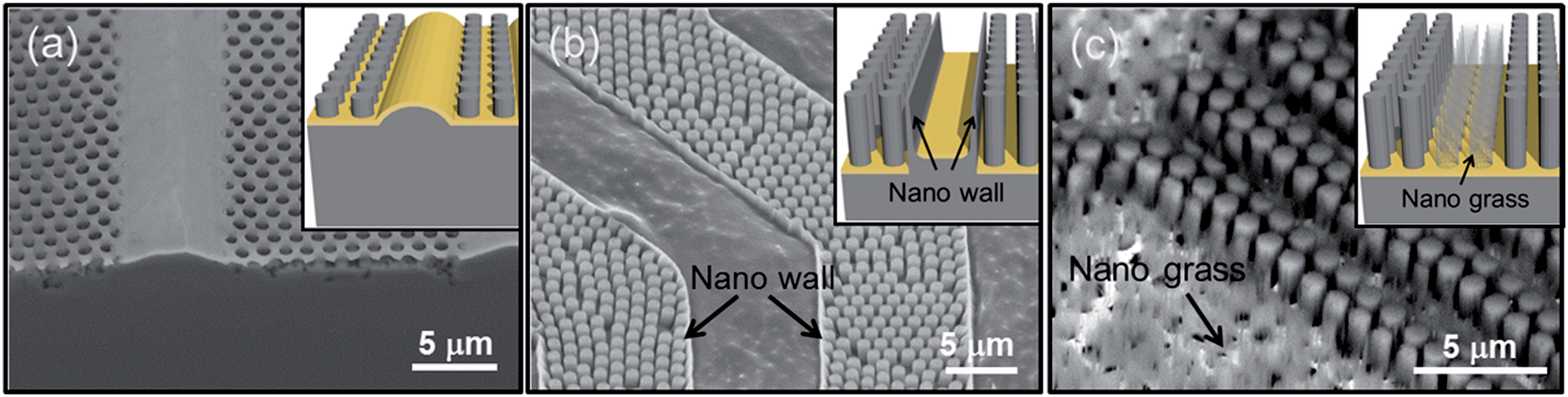 | ||
| Fig. 2 SEM images of the nanostructures obtained after MaCE using (a) type I, (b) type II and (c) type III catalyst patterns. The insets show the schematic illustration of the corresponding structures. | ||
In wet chemistry, it is known that sufficient liquid exchange is extremely important to achieve a uniform reaction rate. In MaCE, the metal (Au here) serves as a catalyst for the reaction between the silicon and the H2O2–HF mixture; however, the large area coverage of the metal film could also hinder the liquid exchange at the center area (Fig. 3a and b), which eventually leads to a degraded reaction rate. As a result, a ridge-like microstructure was produced in the case of type I Au catalyst pattern (Fig. 2a). Nevertheless, this structure was not attained when type II and type III catalyst films were used. Notably, since both type II and type III catalyst films were patterned through a two-step deposition method, in this case, it is likely to form boundary defects/cracks between the two deposited layers (Fig. 3c1 and d1). As presented in Fig. 3c, lateral cracks appeared between the first and the second metal layer, especially when the first-deposited metal patterns had tilted edges (induced by the sloped photoresist edges). Consequently, the second metal layer tends to dissociate from the first layer during the etching due to the stress induced by different etching speeds. This way, the meshed region was etched much faster due to better solution exchanges. In contrast, the continuous covered region showed a slower etching rate. Actually, on further manipulating the pattern to a larger dimension, the etching rate over the micropatterns was also degraded with a distribution slower at the middle and faster at the edges, depending on the liquid exchange ability and pattern size (ESI, Fig. S3†). Due to the deteriorated etching rate, the cracked metal film was not able to fully cover the etched silicon surface when the etching progressed further because of the increased surface area. The uncovered regions were eventually evolved into continuous nanowalls, as depicted in the obtained samples (Fig. 2b). Similarly, in the type III metal patterns, there was also a tendency to form small cracks between the two deposited metal layers at the hole edges of the nanomesh, as illustrated in Fig. 3d. On the one hand, these cracks can favor the solution exchange and thus yield a more uniform etching rate over the entire catalyst covered region; on the other hand, they can also result in the incomplete etching of the designed structures, thus forming arrays of nano-grasses (Fig. 2c). Importantly, all the different thickness selections for the two metal layers can influence the morphology of the nanograsses. It seems that when the second metal layer is thinner than the first metal layer, the obtained nanograsses were thicker in the diameter (ESI, Fig. S4a and b†), which presumably resulted from the larger cracks due to the metal insufficiently filling-up into the holes of the first mesh layer. In contrast, when the second metal layer got thicker than the first layer, there were only very small cracks existing in the metal film at the micro-patterned area, and the nanograss became thin and sparsely distributed (ESI, Fig. S4c†). Moreover, as the liquid exchange ability at some locations were severely decreased due to the coverage of the second metal layer, the etching rate turned out to vary over the different locations and the etching interface became uneven, leading to a crumpled metal film and decreased cross-sectional etching area. As a result, the nanopillar blocks were tapered. With the structures obtained above, we can further control their morphologies by applying the catalyst-free isotropic/anisotropic chemical etching. For instance, by immersing the type III catalyst derived samples in a KOH solution at 90 °C, we can remove the nanograss and achieve various hierarchically configured, high-aspect-ratio nanopillar arrays, as shown in Fig. 4.
 | ||
| Fig. 3 (a) Schematic illustration showing the different etching rates due to the different solution permeabilities at different locations. (b–d) Schematic illustrations and SEM images showing the crack formations in type I, type II and type III catalyst patterns, respectively. | ||
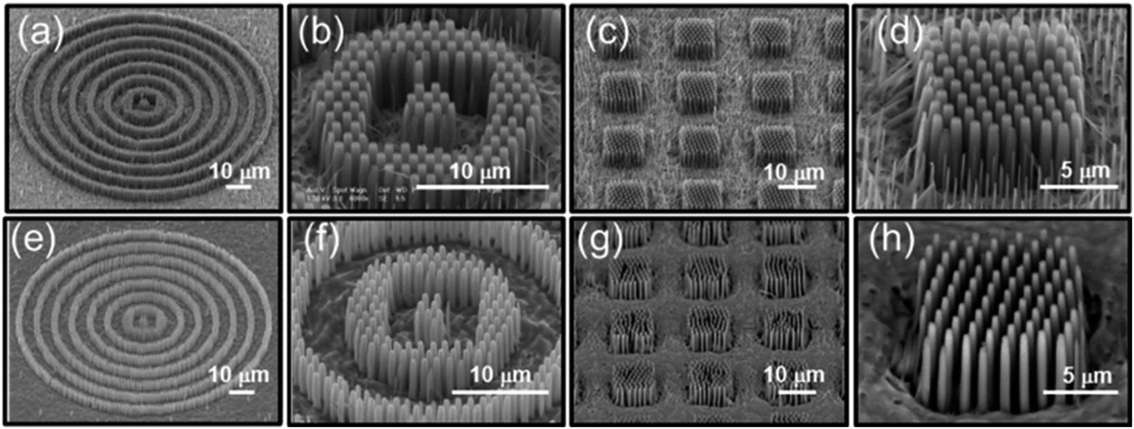 | ||
| Fig. 4 SEM images of the various hierarchical nanostructures before (a–d) and after (e–h) removal of the nanograss. | ||
In addition to the positive nanostructures, nanohole-based negative hierarchical nanostructures could also be useful for many applications. In order to fabricate these negative structures, patterned Au nanodisk arrays were fabricated as the catalyst on silicon. These Au nanodisks can be obtained by utilizing Ar plasma etching/sputtering with PS nanospheres as the etching masks.23–25 To integrate micro-scale patterns into the disk arrays, we first fabricated a thin layer of Cr micropatterns on the silicon wafer using conventional photolithography before the deposition of the Au film (Fig. 5a). As Cr is durable to the Ar plasma, it remains intact during the Au disk fabrication. Moreover, as Cr is inactive in MaCE, it can serve as a blocking layer for the anisotropic etching. Then, the sample was placed in the HF–H2O2 etchant solution, and the Au disks, which were not covered by Cr, could initiate the chemical etching and yield nanohole structures (Fig. 5b). Finally, Cr and Au could be completely removed, leaving hierarchical nanohole arrays with a very smooth surface. All of these nanostructures could be used as replica modes to fabricate inverted hierarchical nanostructures, and the smooth surface could be advantageous for the release of the replicated layer.
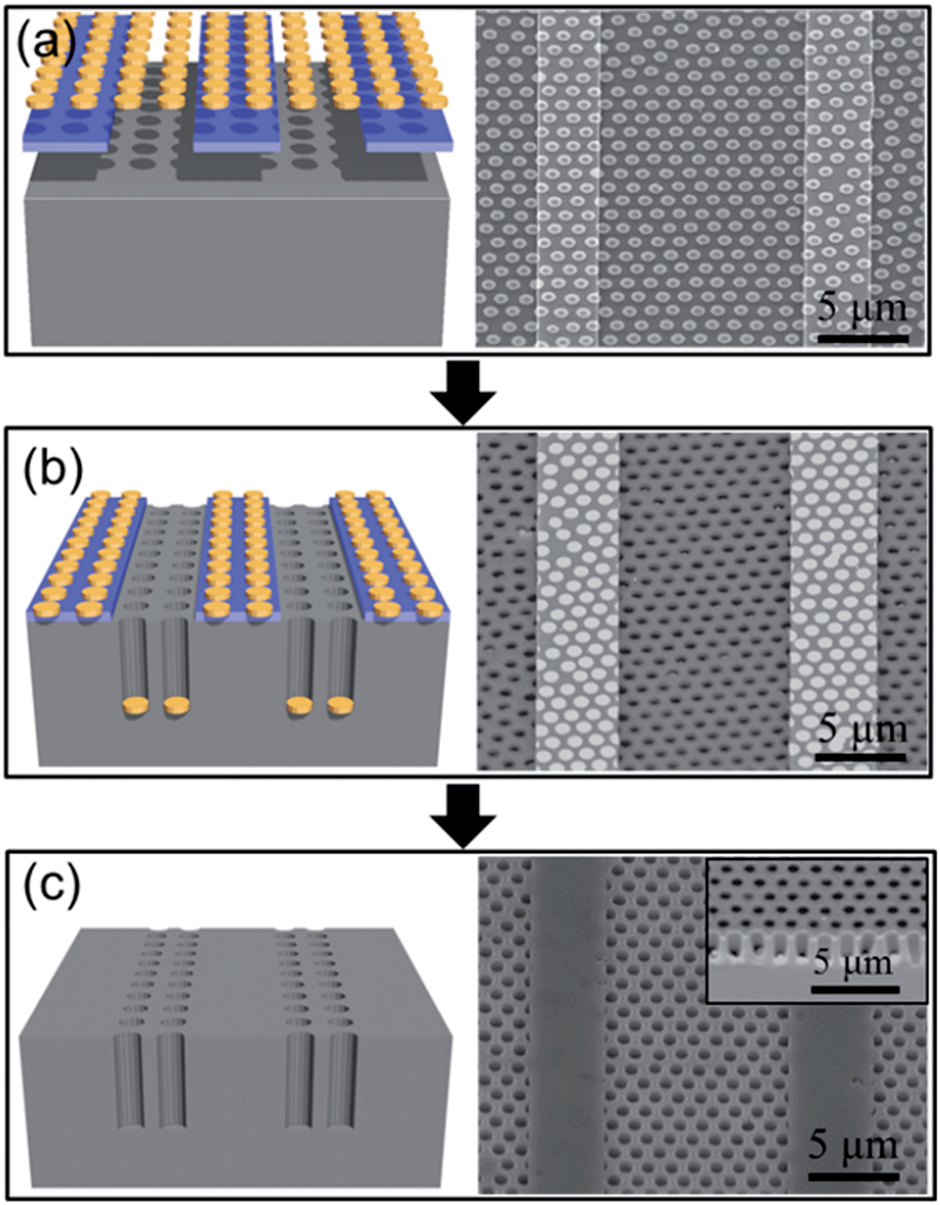 | ||
| Fig. 5 Fabrications of hierarchical negative nanostructures. (a) Deposition of Au nanodisk arrays on a (100) silicon surface with Cr micropatterns, (b) after MaCE and (c) obtaining patterned nanohole arrays after the Cr and Au removal. | ||
Conclusions
In conclusion, we present a low-cost approach to fabricate hierarchical arranged silicon nanostructures by combining MaCE with nanosphere lithography and conventional photolithography. Through the controllable depositions of the metal catalyst films, we can achieve different interesting nanostructures like nanowalls and nanograsses at predefined positions among nanopillar arrays. We have also successfully fabricated hierarchical negative structures by changing the catalyst shape. Moreover, the morphology of the obtained nanostructures could be further manipulated by employing isotropic chemical etching. All these micro/nano hierarchical silicon structures can provide interesting platforms to explore the interplay between the structures and the biological cell attachment behavior and may also find fascinating applications in optoelectronics, photonic devices and bulk lab-on-chip systems.Acknowledgements
This research was financially supported by the City University of Hong Kong (Project no. 9667086), the National Natural Science Foundation of China (Grant number 51202205), the Guangdong National Science Foundation (Grant number S2012010010725), the Science Technology and Innovation Committee of Shenzhen Municipality (Grant number JCYJ20120618140624228), and it was also supported by a grant from the Shenzhen Research Institute, City University of Hong Kong.Notes and references
- S. Jeong, E. C. Garnett, S. Wang, Z. Yu, S. Fan, M. L. Brongersma, M. D. McGehee and Y. Cui, Nano Lett., 2012, 12, 2971–2976 CrossRef CAS PubMed.
- W.-R. Wei, M.-L. Tsai, S.-T. Ho, S.-H. Tai, C.-R. Ho, S.-H. Tsai, C.-W. Liu, R.-J. Chung and J.-H. He, Nano Lett., 2013, 13, 3658–3663 CrossRef CAS PubMed.
- B.-S. Song, S. Noda, T. Asano and Y. Akahane, Nat. Mater., 2005, 4, 207–210 CrossRef CAS.
- B. Corcoran, C. Monat, C. Grillet, D. J. Moss, B. J. Eggleton, T. P. White, L. O'Faolain and T. F. Krauss, Nat. Photonics, 2009, 3, 206–210 CrossRef CAS.
- A. Shakoor, R. Lo Savio, P. Cardile, S. L. Portalupi, D. Gerace, K. Welna, S. Boninelli, G. Franzò, F. Priolo, T. F. Krauss, M. Galli and L. O'Faolain, Laser Photonics Rev., 2013, 7, 114–121 CrossRef CAS.
- F. Priolo, T. Gregorkiewicz, M. Galli and T. F. Krauss, Nat. Nanotechnol., 2014, 9, 19–32 CrossRef CAS PubMed.
- R. A. Potyrailo, H. Ghiradella, A. Vertiatchikh, K. Dovidenko, J. R. Cournoyer and E. Olson, Nat. Photonics, 2007, 1, 123–128 CrossRef CAS.
- S. Y. Kim, J. Yu, S. J. Son and J. Min, Ultramicroscopy, 2010, 110, 659–665 CrossRef CAS PubMed.
- K. Kuwabara, M. Ogino, T. Ando and A. Miyauchi, Appl. Phys. Lett., 2008, 93, 033904 CrossRef.
- J. Tan and W. M. Saltzman, Biomaterials, 2004, 25, 3593–3601 CrossRef CAS PubMed.
- A. Ranella, M. Barberoglou, S. Bakogianni, C. Fotakis and E. Stratakis, Acta Biomater., 2010, 6, 2711–2720 CrossRef CAS PubMed.
- M. Bassu, S. Surdo, L. M. Strambini and G. Barillaro, Adv. Funct. Mater., 2012, 22, 1222–1228 CrossRef CAS.
- G. Polito, S. Surdo, V. Robbiano, G. Tregnago, F. Cacialli and G. Barillaro, Adv. Opt. Mater., 2013, 1, 894–898 CrossRef.
- X. Li and P. W. Bohn, Appl. Phys. Lett., 2000, 77, 2572 CrossRef CAS.
- X. Li, Curr. Opin. Solid State Mater. Sci., 2012, 16, 71–81 CrossRef CAS.
- Z. Huang, N. Geyer, P. Werner, J. de Boor and U. Gösele, Adv. Mater., 2011, 23, 285–308 CrossRef CAS PubMed.
- C. Chang and A. Sakdinawat, Nat. Commun., 2014, 5, 4243 CAS.
- H. Lin, H.-Y. Cheung, F. Xiu, F. Wang, S. Yip, N. Han, T. Hung, J. Zhou, J. C. Ho and C.-Y. Wong, J. Mater. Chem. A, 2013, 1, 9942 CAS.
- H. Lin, F. Xiu, M. Fang, S. Yip and H. Cheung, ACS Nano, 2014, 8, 3752–3760 CrossRef CAS PubMed.
- H. Han, Z. Huang and W. Lee, Nano Today, 2014, 9, 271–304 CrossRef CAS.
- J. Kim, H. Han, Y. H. Kim, S.-H. Choi, J.-C. Kim and W. Lee, ACS Nano, 2011, 5, 3222–3229 CrossRef CAS PubMed.
- J. Kim, Y. H. Kim, S.-H. Choi and W. Lee, ACS Nano, 2011, 5, 5242–5248 CrossRef CAS PubMed.
- P. Hanarp, M. Käll and D. Sutherland, J. Phys. Chem. B, 2003, 107, 5768–5772 CrossRef CAS.
- Y. B. Zheng, B. K. Juluri, X. Mao, T. R. Walker and T. J. Huang, J. Appl. Phys., 2008, 103, 014308 CrossRef.
- F. Liu, M. M. Wong, S. Chiu, H. Lin, J. C. Ho and S. W. Pang, Biosens. Bioelectron., 2014, 55, 141–148 CrossRef CAS PubMed.
Footnotes |
| † Electronic supplementary information (ESI) available. See DOI: 10.1039/c4ra06172a |
| ‡ These authors contributed equally to this work. |
| This journal is © The Royal Society of Chemistry 2014 |