Electroless nanowelding of silver nanowires at room temperature

Chih-Jui Nia and Franklin Chau-Nan Hong*abc
aDepartment of Chemical Engineering, National Cheng Kung University, 1 University Road, Tainan 70101, Taiwan, Republic of China
bCenter for Micro/Nano Science and Technology, National Cheng Kung University, 1 University Road, Tainan 70101, Taiwan, Republic of China
cAdvanced Optoelectronic Technology Center, National Cheng Kung University, 1 University Road, Tainan 70101, Taiwan, Republic of China. E-mail: hong@mail.ncku.edu.tw

Received 23rd June 2014 , Accepted 15th August 2014

First published on 18th August 2014


Abstract

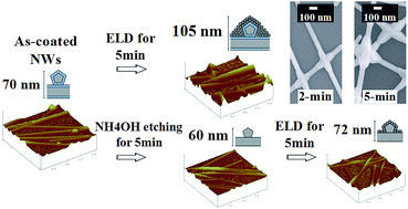
Silver nanowires (Ag NWs) using polyvinylpyrrolidone (PVP) surfactants were coated on either polyethylene terephthalate (PET) or glass substrates. The resistance of the Ag NW film was very high due to the PVP molecules wrapping around the Ag NWs and preventing good electrical contacts between them. We performed an Ag electroless deposition (ELD) on the Ag NW film at room temperature and achieved the welding of Ag NWs by enhancing the deposition of Ag right at the junctions of the two crossing wires. The welding of Ag NWs drastically reduced the sheet resistance (Rsh) of the film from 17[thin space (1/6-em)]000 to 20 ohm sq−1 for only a 2 min treatment. By conducting the Ag ELD on the PVP-removed Ag NW film annealed at 200 °C, we showed that the PVP molecules concentrated at the junctions were responsible for the nanowelding behavior. In addition, both ethylenediamine (EDA) and ammonium hydroxide (NH4OH) could mildly etch the Ag NWs to remove PVP from the wires at room temperature, improving the contacts between Ag NWs and thus reducing the Rsh of the Ag NW film. An organic light emitting diode with ELD-treated Ag NW film was prepared to demonstrate the applicability of the nanowelding technique for conductivity enhancement. The better performance of the device based on ELD-treated Ag NW film compared with that on Ag thin film was due to the higher degree of light transmittance and work function of the Ag NWs.


Introduction

Silver nanowires (Ag NWs) have often been coated on flexible substrates to fabricate transparent conductive films1–4 for flexible devices such as organic photovoltaic cells,5–8 organic light emitting diode devices (OLEDs),9–11 etc., due to their unique advantages that include flexibility, high conductivity, low temperature processes, and facile fabrication, as compared to the most commonly used material, indium tin oxide (ITO). A conducting network can be obtained by the decomposition of polyvinylpyrrolidone (PVP) surfactants1,6 capped around NWs with a thickness of 1 to 3 nm.5 The partial decomposition of PVP by heating allows the Ag NWs to connect and fuse together. The typical range of heating temperature is from 180 to 200 °C for several tens of minutes;5 thus, the fabrication is restricted to some special heat-resistant substrates. However, the thermal process possesses some drawbacks. It is time-consuming and induces shrinkage in many flexible plastic substrates. An electrochemical method1 was recently reported to reduce the wire-to-wire junction resistance by immersing Ag NW film in a boiling HAuCl4 aqueous solution. This simple galvanic displacement process turns the network of pure Ag NWs into a network of gold-coated Ag NWs. Garnett et al.12 demonstrated a light-induced plasmonic nanowelding technique to assemble Ag NWs into large interconnected networks. The process was performed using tungsten halogen lamps at a power density of 30 W cm−2 in nitrogen ambient. Large field enhancement could occur in the nanoscale gap between two crossing wires to weld them together.

In this study, we introduced a nanowelding method to significantly reduce the sheet resistance (Rsh) of the Ag NW film at room temperature by the electroless deposition of silver (Ag). We found that PVP molecules could activate the Ag ELD, and the concentrated PVP molecules at the junctions of two crossing Ag NWs were found to induce the selective Ag deposition at the junctions. Ethylenediamine (EDA) and ammonium hydroxide (NH4OH) could mildly etch the Ag NWs and thus remove PVP from the NWs, causing the reduction of the Rsh of the Ag NW film. Then, after the ELD treatment of the PVP-removed Ag NWs, the Ag deposition was highly uniform over the full lengths of the wires. The results confirmed the promotion of PVP for Ag deposition during the ELD process. To demonstrate the potential of this nanowelding method for preparing transparent conductive films, an OLED device was fabricated by using the ELD-treated Ag NW film as an anode. The OLED performance revealed that the nanowelding technique is highly effective in manufacturing transparent conductive films for optoelectronic device applications.

Experimental

Synthesis of silver nanowires

All chemicals were purchased from Sigma Aldrich. The Ag NW ink was prepared using a simplified polyol method.13,14 As in a typical Ag NW synthesis situation, 0.255 g of silver nitrate was dissolved in 60 mL ethylene glycol (EG) solution containing 1.25 g PVP (Mw = 40[thin space (1/6-em)]000) and 0.004 g sodium chloride. The mixture was placed in an oven at 160 °C for 2 h. After synthesis, the solution was poured into excess acetone (acetone/EG = 5/1 v/v) and centrifuged at 6000 rpm for 10 min, followed by the removal of the supernatant solvent. The product was finally collected after water washing and centrifugation at 6000 rpm for several cycles to remove most of the PVP and EG.

Fabrication of silver nanowire film

Ag NWs were dispersed in pure water without the addition of methanol or ethanol, which is usually added to adjust the surface tension of the ink. Since PVP is better dissolved in water than it is in methanol, Ag NWs bound by PVP tend to be more stable in water than in methanol. However, the slight dewetting of the Ag NW aqueous ink on the polyethylene terephthalate (PET) substrate induced cracks in the Ag NW film. Therefore, to improve the wettability of the aqueous Ag NW ink to PET substrates, the substrates were always pretreated with oxygen plasma at 70 W for 30 s at 100 mTorr. For the purpose of preparing the Ag NW film, a droplet of 1.5 wt% Ag NW ink was placed on either the oxidized PET or glass substrate and rolled using a wire bar (SHEEN Inc.). A uniform, thin layer of Ag NW ink with a 6 μm wet thickness could be coated on the substrate by choosing an appropriate wire bar (wire spacing: 300/inch). The wet film was dried out quickly in the atmosphere without heating.

Electroless deposition

Ag electroless deposition on the coated Ag NW film was performed to improve the contacts between the crossing Ag NWs. The as-coated Ag NW film on the PET or the glass substrate was immersed in the mixture of an Ag ion complex solution and a reducing agent solution at room temperature. The Ag ion complex solution was composed of 6 × 10⁻³ M silver nitrate and 3.6 × 10⁻² M EDA in 250 mL of water. The reducing agent solution was composed of 7 × 10⁻² M potassium sodium tartrate (Rochelle salt) and 7.4 × 10⁻⁵ M 3,5-diiodotyrosine (DIT) in 250 mL of water. These two solutions were then well-mixed to form the ELD bath solution right before the Ag deposition. To understand the effect of PVP on the ELD behaviour of the Ag NWs, the NW film on the glass was annealed at 200 °C for 40 min to decompose the PVP and then placed in the ELD bath at room temperature.

Wet etching

Typical wet etching experiments were carried out at room temperature by immersing the as-coated Ag NW film on PET into an ethylenediamine aqueous solution and an ammonium hydroxide solution, respectively, of various concentrations for several minutes.

Nanowire film characterization

A scanning electron microscope (FE-SEM, JEOL JSM-6700F) was employed to characterize the morphology and composition of the Ag NW films. The surface profiles of a single Ag NW as well as the crossing junctions of Ag NWs were measured using tapping mode atomic force microscopy (AFM) (Digital Instruments, Santa Barbara, CA, NS3a-2/MMAFM) using a Si probe (Innovative Solutions Bulgaria Ltd., Bulgaria) with a nominal force constant of 5 N m−1. The AFM images were recorded at a typical scan speed of 0.5 Hz over an area of 2 × 2 μm2. The sheet resistance of the Ag NW film was measured with a 4-point probe using a Keithley 2400 meter.

OLED fabrication and optoelectronic characterization

The glass substrates were cleaned sequentially by ultrasonication in a detergent solution, deionized water, isopropyl alcohol and ethanol for 15 min each. The Ag NW film coated on glass was treated with ELD and patterned by 3M tape adhesion, then spin-coated with 3 wt% N,N′-bis(naphthalene-1-yl)-N,N′-bis(phenyl)benzidine (NPB) in 1,2-dichloroethane at 2000 rpm for 150 s. The device structure, which consisted of NPB (25 nm), tris-(8-hydroxyquinoline)-aluminum (Alq3, 50 nm), 2,9-dimethyl-4,7-diphenyl-1,10-phenanthroline (BCP, 10 nm), lithium fluoride (LiF, 1 nm), and aluminum (Al, 35 nm), was deposited subsequently by thermal evaporation in a vacuum chamber with a base pressure of 10−7 Torr. The active area of the device was approximately 3 mm2. The thickness of the solution-processed NPB on a blank glass substrate was 100 nm, as measured by a Tencor alpha-step surface profiler. The current–voltage (IV) and luminance–voltage (LV) characteristics of the devices were all measured at room ambient and temperature with a source meter (Keithley-2400) and a luminance meter (Minolta LS-110). The work functions were measured by the photoelectron spectrometer in air (Hitachi-AC2) with gold foil (4.8 eV) as a reference.

Results and discussion

Electroless deposition process

Ag NW aqueous suspension was coated as an ink on a PET substrate of 100 cm2 in area using a wire bar. As shown in Fig. 1(a) and (b), the PET film coated with the Ag NW layer showed high transparency with a light transmittance of 89% at 550 nm. The SEM image of the Ag NWs coated on PET with a M/A (mass/area) of 41 mg m−2 in Fig. 1(c) showed that almost all of the Ag NWs crossed each other, and rare nanoparticles can be observed. The Ag NWs employed were 30–50 nm in diameter and 3–10 μm in length. The Rsh of the as-coated Ag NW film was about 17[thin space (1/6-em)]000 ohm sq−1.
image file: c4ra06138a-f1.tif
Fig. 1 (a) A photograph of bare PET and PET coated with Ag NW film. (b) A uniform and flexible Ag NW film on PET substrate. (c) A SEM image of the Ag NW film on PET.

To improve the conductivity of the Ag NW film, two methods have been reported. The first one is to increase the density of the Ag NWs in the film. However, a denser network of NWs blocks light transmission. The other method is to remove PVP macromolecules from the surface of the NWs after coating. PVP is a surfactant necessary for controlling one-dimensional (1D) growths and avoiding agglomeration during the synthesis of Ag NWs. PVP molecules are adsorbed on the NWs and are inseparable from them during centrifugal separation. Fortunately, the PVP bonded on the NWs can be decomposed at a high temperature. The lowest annealing temperature reported to decompose PVP for achieving a low Rsh is 180 °C.5 However, such a high temperature heating process is not compatible with most optic plastic substrates. We attempted to lower the annealing temperature down to 100 °C. After heating for 2 h, the Rsh of the Ag NWs on PET decreased from several thousands to 800 ohm sq−1. However, further heating for more than 2 h led to an increase of Rsh from 800 back to several thousand ohm sq−1 because of damage to the PET substrate. As a result, a low temperature process to reduce the contact resistance between Ag NWs is required for the fabrication of Ag NW films on the low cost optic plastics like PET. Herein is a report on the application of a low temperature Ag electroless deposition process to improve the conductivity of Ag NW films.

The SEM images of the as-coated Ag NW films treated with Ag ELD process for various periods of time are shown in Fig. 2. The diameters of Ag NWs in general increased gradually with the increase in the deposition time. However, as shown in Fig. 2(c), the Ag ELD process for 1 min began to indicate clearly that more Ag was deposited on the junctions of the two crossing Ag NWs than in the area away from the junctions of the NWs. As the deposition time was increased to 2, 5, and 10 min in Fig. 2(d–f), respectively, the amount of Ag deposited on the junctions of the Ag NWs increased further with the increase in deposition time. As shown in Fig. 2(g), the TEM image of the sample for Fig. 2(e) also confirmed the enhanced Ag ELD at the junctions of the NWs. The value of Rsh for the Ag NW film treated with the Ag ELD processes was measured, and plotted in Fig. 2(h) versus the time period of the ELD treatment. The corresponding light transmittance is also shown using the coordinate on the right axis. After the ELD process for 0.5 min, the Rsh of the Ag NW film decreased from 17[thin space (1/6-em)]000 to 4000 ohm sq−1 with a drop in light transmittance from 89% to 85% at 550 nm. By further increasing the deposition time to 2 min, the film Rsh was significantly decreased (almost exponentially with the deposition time) to 20 ohm sq−1, with only a slight drop of light transmittance to 80% at 550 nm. Further increase in the deposition time did not reduce the Rsh much, but the light transmittance decreased significantly. Evidently, the enhanced Ag ELD at the crossing junctions effectively reduced the contact resistance between the Ag NWs.


image file: c4ra06138a-f2.tif
Fig. 2 SEM images of the as-coated Ag NW films treated with the Ag ELD process for (a) 0 min, (b) 0.5 min, (c) 1 min, (d) 2 min, (e) 5 min, and (f) 10 min. (g) A TEM image of the as-coated Ag NWs treated with the ELD process for 5 min. (h) The sheet resistance (left) and light transmittance (right) of the Ag NW films treated with the Ag ELD process for various time periods.

To understand why the Ag ELD was enhanced at the crossing junctions of Ag NWs, we studied the effects of PVP on the behaviour of Ag deposition, since PVP was always used for controlling the 1D Ag NW growth and remained adsorbed on the Ag NWs even after washing and centrifugation before coating. In addition, PVP has also been used as a reducing agent in the reduction of silver and gold.15,16 Therefore, the presence of PVP might play a role in Ag ELD. The effect of PVP on the ELD of Ag NW films was thus investigated.

For the purpose of removing the PVP molecules adsorbed on the Ag NWs, the as-coated Ag NW film was first annealed at 200 °C for 40 min. Then, the Ag ELD on the annealed Ag NW film was performed. The SEM images of the annealed Ag NWs after ELD for various time periods are shown in Fig. 3(a)–(d). Since PVP could be partially decomposed by annealing,5 the annealed NWs should be free of PVP and thus the Ag ELD on the annealed NWs was actually performed on the PVP-free Ag NWs. As shown in Fig. 3(a)–(d), the Ag deposition on the PVP-free Ag NWs was highly uniform over the full lengths of the NWs for various deposition periods from 1 to 10 min. As described earlier in Fig. 2, the Ag deposition on the as-coated Ag NWs (with PVP adsorbed) was particularly enhanced at the junctions of NWs. The results suggested that, for the as-coated Ag NWs, the adsorbed PVP might be responsible for the enhanced Ag ELD at the crossing junctions.


image file: c4ra06138a-f3.tif
Fig. 3 SEM images of the as-coated Ag NWs annealed at 200 °C for 40 min and then treated with Ag ELD for (a) 1 min, (b) 2 min, (c) 5 min, and (d) 10 min. (e) The as-coated Ag NWs annealed at 200 °C for 40 min, then immersed in PVP solution and further treated with Ag ELD for 5 min.

Furthermore, for the as-coated Ag NW film shown in Fig. 2, the 2 min Ag ELD decreased the Rsh of the as-coated Ag NW film enormously from 17[thin space (1/6-em)]000 to 20 ohm sq−1. However, for the annealed Ag NW film, the 2 min Ag ELD had almost no effect on the Rsh of the annealed Ag NW film (varied from 17 ohm sq−1 to 15 ohm sq−1 by 2 min Ag ELD). For the as-coated Ag NWs, the fast drop of Rsh by 2 min ELD was due to the selective welding of Ag NWs by enhancing Ag deposition at the junctions to improve the contacts between two Ag NWs, which were originally isolated from each other by adsorbed PVP molecules before the ELD process. The Rsh of the annealed Ag NWs was not affected by 2 min ELD, since the conductivity across the junctions was already good due to the removal of PVP by annealing and the selective welding at the junctions by 2 min Ag ELD was completely absent.

By further immersing the annealed, PVP-free, Ag NW film into the PVP solution to adsorb PVP back to the Ag NWs, the 5 min ELD on the Ag NW film re-adsorbed with PVP molecules resulted in the selective welding at the junctions of NWs again, as shown in Fig. 3(e). The results confirmed that the PVP molecules adsorbed on the Ag NWs should be responsible for the enhanced Ag ELD at the NW junctions.

Wet etching process

EDA could react with Ag ions to form Ag-EDA complexes, and we found that EDA aqueous solution could mildly etch the surface of Ag NWs. Therefore, EDA was used to remove the PVP molecules adsorbed on the surface of Ag NWs by slightly etching away the surface Ag atoms on the NWs through the formation of Ag-EDA complexes. The as-coated Ag NW film was immersed in the EDA aqueous solution (16.7 mM) for various time periods. Fig. 4 shows the relationship between the Rsh and the etching time. The Rsh of the Ag NW films decreased first with increasing the etching time, and then increased when the etching time was longer than 15 min. As shown in the inset of Fig. 4, the surface of Ag NWs became rough after etching. The results imply that the removal of PVP by EDA will cause the reduction of the Rsh in the Ag NW film due to the improved contacts between Ag NWs. However, the long-time etching (>15 min) will cause the increase of the Rsh in the Ag NW film due to the shrinkage of the cross sections of Ag NWs by etching.
image file: c4ra06138a-f4.tif
Fig. 4 Rsh of the as-coated Ag NW films treated with 16.7 mM EDA for various time periods. The inserted SEM image is the as-coated Ag NWs treated with 16.7 mM EDA for 15 min.

It was suspected that the removal of PVP molecules at the junctions of Ag NWs was not complete, since the Rsh of the EDA-etched Ag NW film shown in Fig. 4 remained high. The NH4OH aqueous solution was further attempted as another etchant17 to remove the PVP adsorbed on the surface of Ag NWs. Fig. 5 shows the Rsh of Ag NW films treated with NH4OH solutions with various concentrations and times. For each concentration of NH4OH solution, the Rsh of the film always decreased first with increasing the etching time to reach the lowest value, and then increased when the etching time increased further. The etching time with the lowest Rsh of the Ag NW films is highly related to the concentration of the NH4OH solution. After immersing in 293, 29.3, and 16.7 mM of NH4OH solution, the minimum Rsh was obtained when the etching time was 0.5, 1.0, and 2.0 min, respectively. Considering the surface morphology of the Ag NWs, they became rougher when the etching time and concentration increased. The NWs even turned into discontinuous sections under a 10 min treatment in 29.3 mM NH4OH solution. The same effect was also observed when treating in the 16.7 mM NH4OH solution. P. Yang et al.18 showed that the etching of Ag {100} faces proceeds rapidly with the addition of increasing amounts of etchant solution (9[thin space (1/6-em)]:[thin space (1/6-em)]1 NH4OH–H2O2), whereas very little etching occurs on the Ag {111} faces. As shown in Fig. 5, the Rsh of the Ag NW film was improved from several thousands to 100 ohm sq−1 for 2 min of etching. If the etching was continued in 16.7 mM NH4OH for longer than 2 min, the Rsh of the NW film started to increase due to the etching of NWs shrinking their cross sections.


image file: c4ra06138a-f5.tif
Fig. 5 Rsh of the Ag NW films treated with NH4OH solutions of various concentrations for various time periods. The inserted SEM images are the surface morphologies of the as-coated Ag NW films after immersion in an NH4OH solution under various conditions.

Fig. 6 shows the light transmittance of Ag NW films treated with 16.7 mM NH4OH solution for various time periods. Slight increase in light transmittance with increasing the etching time indicates that some parts of the Ag NWs were etched away by the NH4OH solution.


image file: c4ra06138a-f6.tif
Fig. 6 Light transmittance of the as-coated Ag NW films treated with 16.7 mM NH4OH solution for various time periods. The transmittance at 550 nm slightly increased to 92% after etching for 15 min.

The Ag ELD process was then conducted for 5 min on the Ag NW films treated with 16.7 mM NH4OH solution for various time periods in order to study the behaviour of Ag deposition on the NWs after etching. As shown in Fig. 7(a)–(c), the concentrated deposition of Ag at the NW junctions was observed for the short etching times, 0.5, 1.0 and 2.0 min. Slight amounts of PVP might be left on the NW junctions after etching for such a short time period. However, as shown in Fig. 7(d) and (e), Ag deposition was highly uniform over the NWs of the Ag NW film etched for 5 or 10 min. Fig. 8 shows that the Rsh of the Ag NW film was first decreased with increasing the etching time due to the removal of PVP improving the contacts of NW junctions, and then increased with further increasing the etching time due to the damage of Ag NWs. Following the NH4OH etching for various time periods, the 5 min ELD always reduced the Rsh of the Ag NW film to a very low value around 10–20 ohm sq−1. The ELD seems more effective than the NH4OH or EDA etching in reducing the Rsh of the Ag NW film to a value below 20 ohm sq−1.


image file: c4ra06138a-f7.tif
Fig. 7 SEM images of the Ag NWs treated with 16.7 mM NH4OH for (a) 0.5 min, (b) 1 min, (c) 2 min, (d) 5 min, and (e) 10 min and then ELD for 5 min.

image file: c4ra06138a-f8.tif
Fig. 8 Rsh of the Ag NW films treated with NH4OH for various time periods before and after 5 min ELD.

With mild etching ability, the NH4OH and EDA etching for short periods of time could remove most of PVP from the surface of NWs by maintaining a small amount of PVP on the junctions of NWs. The PVP molecules were concentrated at and not easily removed from the junctions. The subsequent ELD could thus induce the nanowelding effect without thickening the Ag NWs, as shown in Fig. 7(a)–(c). Therefore, the light transmittance of the Ag NW film treated with first the short time etching and then the ELD could remain high. By treating the as-coated Ag NW film with first 2 min NH4OH etching and then 2 min ELD, the Rsh and the light transmittance were 14 ± 0.9 ohm sq−1 and 83% at 550 nm, respectively. For comparison, the Rsh and the light transmittance of the as-coated Ag NW film treated with 2 min ELD only were 20 ± 6.0 ohm sq−1 and 80% at 550 nm, respectively. Our results showed that the best electrical and optical properties of the Ag NW films could be obtained by carefully performing the wet etching process before the nanowelding.

AFM was further employed to characterize the nanowelding effect. According to the results measured by AFM, more silver will be deposited on the as-coated Ag NWs compared with the ammonia-etched wires, especially at the junctions, during the ELD process. A schematic illustration is shown in Fig. 9. The thickness of the single wire and the junction for the as-coated Ag NWs were 34 ± 1.2 nm and 70 ± 3.8 nm, respectively. After the 5 min ELD process, the thickness of the single wire and the junction became 46 ± 3.0 nm and 105 ± 10.3 nm, respectively. Furthermore, concerning the etched Ag NWs treated with NH4OH for 5 min, the thicknesses of the single wire and the junction were 34 ± 2.8 nm and 60 ± 6.7 nm, respectively. The values became 38 ± 1.3 nm and 72 ± 5.0 nm after the 5 min ELD process. The phenomenon of selective Ag deposition at the junctions for the as-coated NWs may be related to the promotion of PVP bonded on the Ag NW. The single nanowire of the as-coated film was thicker than that of the etched one after ELD. Considering the junction of the two crossing wires after ELD, the increase in thickness for the as-coated film was much larger than that for the etched one. These results confirmed that the adsorbed PVP molecules enhance the Ag ELD. In electrochemical synthesis of Ag nanoparticles, several studies have indicated that the donated lone pairs of both nitrogen and oxygen atoms in the polar groups of one PVP unit may occupy two sp orbitals of Ag ions to form a metal complex.19–21 The ligands of C–N and C[double bond, length as m-dash]O in PVP contribute more electronic density to the sp orbital of Ag ions, so the Ag ions in the Ag+-PVP complex may obtain electrons and become easily reduced. In addition, some references have reported that PVP also acts as a weak reducing agent to reduce Ag ions.16 Thus, the silver was accumulated selectively at the junction during the ELD process due to the presence of PVP.


image file: c4ra06138a-f9.tif
Fig. 9 Schematic illustration of Ag deposition at the junction of two Ag NWs: (a) with bonded PVP; (b) without bonded PVP.

Performance of the OLED device based on the Ag NW electrode

A general OLED device with the as-coated Ag NW film after 2 min ELD treatment was prepared to demonstrate the feasibility of the nanowelding technique for conductivity enhancement. Fig. 10(a) shows the device structures which consisted of glass/Ag NWs (or Ag film, for comparison)/solution-processed NPB/NPB/Alq3/BCP/LiF/Al. The purpose of the solution-processed NPB layer was to smooth the surface preventing the current leakage and transport the holes from the Ag NWs. In addition, the thickness of the solution-processed NPB film was optimized to prevent the high resistance caused by a thick layer.22,23 Here, we used a 3% NPB solution to spin coat at 2000 rpm for 150 s. Once the concentration of the solution was increased to 5%, the luminance and the current density of the device decreased significantly.
image file: c4ra06138a-f10.tif
Fig. 10 (a) Cross-sectional diagrams of the OLED devices based on the Ag film and the Ag NW film. (b) SEM and (c) AFM images of the ELD-treated Ag NW film with spin-coated NPB. (d) LV and (e) IV characteristics of the OLED devices with the Ag film and the Ag NW film anodes. (f) Work function measurements of the Ag film and the Ag NW film.

Fig. 10(b) and (c) show the SEM and AFM images of the ELD-treated Ag NW film by coating with NPB. The heights at the junctions of the two crossing wires after ELD were about 100 nm because of the selective Ag deposition. Therefore, the thickness of the coated NPB should be slightly over this value to ensure surface flatness. In Fig. 10(c), the roughness (Rq) decreased from 26 to 2.4 nm, indicating a smooth surface. Once a while we could observe a few protrusions in tens-of-nanometer height, where a leakage current in the device might be induced.

Fig. 10(d) shows the luminescence intensity versus the applied voltage (LV). An OLED device, as a comparison, was deposited on the vacuum-deposited Ag thin film under the same conditions. The device with the Ag NW film anode was much brighter than that with the Ag film anode, and the turn-on voltages at 1 cd m−2 were 9.1 and 12.9 V, respectively. The current–voltage (IV) characteristics of the OLED devices with different anodes are shown in Fig. 10(e). A leakage current caused by the protrusions at the surface occurred at low voltages of around 3–4 V for the device with the Ag NW anode. One reason for the superior performance of the device with the Ag NW anode was its higher degree of light transmittance compared with the vacuum-deposited Ag film. The optimized thickness of the Ag film was 15 nm, and the transmittance was only 43% at 550 nm. Since the transmittance was much lower than 80% of the Ag NWs, the Ag film anode has a much lower light extraction efficiency. The other reason is related to the higher work function of the Ag NW anode, which reduces the hole-injection barrier in the anode/organic interface. The work functions of the Ag film and the Ag NWs were both characterized by the photoelectron spectrometer, and the results are shown in Fig. 10(f). The work functions for the Ag film and the Ag NWs were 4.45 and 4.72 eV, respectively. The highest occupied molecular orbital (HOMO) of NPB is generally 5.4 eV. The larger difference between the work function of the Ag film and the HOMO energy level of NPB will create a higher hole-injection barrier, leading to a higher turn-on voltage and worse device performance. The larger work function of the Ag NWs as compared to that of the Ag film has been attributed to the partial formation of silver oxide (5.2 eV, work function) around the surfaces of the nanowires.24 The superior OLED performance using the ELD-treated Ag NWs as an anode revealed that the nanowelding technique improves the transparent conductive properties of the Ag NW film exhibiting potentials for applications to optoelectronic devices.

Conclusions

In summary, the Ag electroless deposition (ELD) on the Ag nanowire (NW) film at room temperature was demonstrated to weld the Ag NWs by selectively enhancing the deposition of Ag right at the junctions of two crossing NWs. The sheet resistance of the film was reduced from 17[thin space (1/6-em)]000 to 20 ohm sq−1 with a slight drop of light transmittance from 89 to 80% at 550 nm by a 2 min ELD treatment. By the Ag ELD on the Ag NW film annealed at 200 °C to remove PVP molecules adsorbed on the NWs, PVP was confirmed to induce the selective deposition of Ag at the junctions of NWs. The ELD process was also performed on the Ag NW films treated with a 16.7 mM NH4OH solution to remove PVP, further verifying the promotion of PVP for Ag ELD to induce the enhanced deposition at the NW junctions. The key advantages of this method include (1) short welding time, (2) avoiding the damage of polymer substrate due to heating, (3) improving the conductivity of the film and (4) retaining the transparency by selective welding at the junctions. A general OLED device was fabricated by using the ELD-treated Ag NW film as an anode to prove the applicability of the nanowelding method. The results showed that the performance of the device with ELD-treated Ag NWs film was better than that with the Ag thin film due to the higher degree of light transmittance and the larger work function for the Ag NWs.

Acknowledgements

The authors gratefully acknowledge the financial support from the National Science Council of Taiwan under grant NSC-99-2221-E-006-197-MY3 and NSC-102-2221-E-006-240-MY3.

Notes and references

  1. L. Hu, H. S. Kim, J.-Y. Lee, P. Peumans and Y. Cui, ACS Nano, 2010, 4, 2955–2963 CrossRef CAS PubMed.
  2. S. De, T. M. Higgins, P. E. Lyons, E. M. Doherty, P. N. Nirmalraj, W. J. Blau, J. J. Boland and J. N. Coleman, ACS Nano, 2009, 3, 1767–1774 CrossRef CAS PubMed.
  3. Y. C. Lu and K. S. Chou, Nanotechnology, 2010, 21, 215707 CrossRef CAS PubMed.
  4. T. Kim, A. Canlier, G. H. Kim, J. Choi, M. Park and S. M. Han, ACS Appl. Mater. Interfaces, 2013, 5, 788–794 CAS.
  5. J.-Y. Lee, S. T. Connor, Y. Cui and P. Peumans, Nano Lett., 2008, 8, 689–692 CrossRef CAS PubMed.
  6. J.-Y. Lee, S. T. Connor, Y. Cui and P. Peumans, Nano Lett., 2010, 10, 1276–1279 CrossRef CAS PubMed.
  7. W. Gaynor, J.-Y. Lee and P. Peumans, ACS Nano, 2010, 4, 30–34 CrossRef CAS PubMed.
  8. D.-S. Leem, A. Edwards, M. Faist, J. Nelson, D. D. C. Bradley and J. C. de Mello, Adv. Mater., 2011, 23, 4371–4375 CrossRef CAS PubMed.
  9. X.-Y. Zeng, Q.-K. Zhang, R.-M. Yu and C.-Z. Lu, Adv. Mater., 2010, 22, 4484–4488 CrossRef CAS PubMed.
  10. T. L. Belenkova, D. Rimmerman, E. Mentovich, H. Gilon, N. Hendler, S. Richter and G. Markovich, J. Mater. Chem., 2012, 22, 24042–24047 RSC.
  11. S. Coskun, E. S. Ates and H. E. Unalan, Nanotechnology, 2013, 24, 125202 CrossRef PubMed.
  12. E. C. Garnett, W. Cai, J. J. Cha, F. Mahmood, S. T. Connor, M. G. Christoforo, Y. Cui, M. D. McGehee and M. L. Brongersma, Nat. Mater., 2012, 11, 241–249 CrossRef CAS PubMed.
  13. B. Wiley, T. Herricks, Y. Sun and Y. Xia, Nano Lett., 2004, 4, 1733–1739 CrossRef CAS.
  14. X. Tang, M. Tsujia, P. Jiang, M. Nishio, S.-M. Jang and S.-H. Yoon, Colloids Surf., A, 2009, 338, 33–39 CrossRef CAS PubMed.
  15. C. E. Hoppe, M. Lazzari, I. Pardinas-Blanco and M. A. Lopez-Quintela, Langmuir, 2006, 22, 7027–7034 CrossRef CAS PubMed.
  16. K. Patel, S. Kapoor, D. P. Dave and T. Mukherjee, J. Chem. Sci., 2005, 117, 53–60 CrossRef CAS.
  17. J.-M. Noël, J. Velmurugan, E. Gökmese and M. V. Mirkin, J. Solid State Electrochem., 2013, 17, 385–389 CrossRef PubMed.
  18. M. J. Mulvihill, X. Y. Ling, J. Henzie and P. Yang, J. Am. Chem. Soc., 2010, 132, 268–274 CrossRef CAS PubMed.
  19. Z. Zhang, B. Zhao and J. Hu, J. Solid State Chem., 1996, 121, 105–110 CrossRef CAS.
  20. I. Pastoriza-Santos and L. M. Liz-Marzan, Langmuir, 2002, 18, 2888–2894 CrossRef CAS.
  21. G. Carotenuto, G. P. Pepe and L. Nicolais, Eur. Phys. J. B, 2000, 16, 11–17 CrossRef CAS.
  22. W. Geens, S. E. Shabeen, B. Wessling, C. J. Brabec, J. Poortmans and N. S. Sariciftci, Org. Electron., 2002, 3, 105–110 CrossRef CAS.
  23. W. Brütting, S. Berleb and A. G. Mückl, Org. Electron., 2001, 2, 1–36 CrossRef.
  24. C.-H. Liu and X. Yu, Nanoscale Res. Lett., 2011, 6, 75 CrossRef PubMed.

This journal is © The Royal Society of Chemistry 2014