
Templated magnesiothermic synthesis of silicon nanotube bundles and their electrochemical performances in lithium ion batteries†
Jingjing Chen,
Miaomiao Liu,
Jing Sun and
Fangfang Xu*
State Key Laboratory of High Performance Ceramics and Superfine Microstructures, Shanghai Institute of Ceramics, Chinese Academy of Sciences, Shanghai, 200050, PR China. E-mail: ffxu@mail.sic.ac.cn; Tel: +86-21-52412574
First published on 28th August 2014
Abstract
Silicon nanotube bundles (Si NBs) have been synthesized on a large scale via a templated magnesiothermic method. Hydroxyapatite (HAP) nanobelt bundles were fabricated and used as a sacrificial template to form silica nanotube bundles (SiO2 NBs) followed by transformation of SiO2 NBs into Si NBs through magnesiothermic reduction. The structure and morphology of the as-prepared Si NBs were examined in detail by XRD, Raman spectroscopy, SEM and TEM. The electrochemical application of Si NBs as an anode in lithium ion batteries (LIBs) has been investigated, which shows a reversible capacity with little fading, outweighing the performance using Si nanoparticles.
1. Introduction
Of all batteries, LIBs are considered to be the most promising energy storage technology due to their long cycle life and high specific capacity.1 However, there are still many challenges to further enhance their performance so as to meet the requirements for efficient hybrid or electric vehicles.2,3 In the past decades, substantial efforts have been made in exploiting silicon-based composites as the anode materials for LIBs,4–8 owing to their excellent merits in high theoretical electrochemical capacity.9 Besides, silicon has a low discharge potential (∼370 mV vs. Li/Li+) which makes it safe and suitable for high-power applications paired with common cathode materials like LiCoO2 and LiMn2O2.10 Nonetheless, the practical application of Si powder is still hindered because of its severe volume expansion/contraction during the alloying and de-alloying reaction with Li+ ions.11 Significant volume change during cycling could result in pulverization and loss of capacity. An effective way to solve this problem is the employment of nanostructure silicon, in which the strain can be relaxed easily without mechanical fracture because of smaller size and available surrounding free space.6,12–15 Consequently, nanostructure silicon ranging from nanowires, nanofilms, nanotubes to nanoparticles and their composites have been exploited to alleviate the structure deterioration efficiently.9,16–21 Especially, one-dimensional tubular nanostructures are highlighted because of their low density and increased surface areas as well as the advantages in improving electrochemical performance and obtaining reversible morphological change.17,22–24Among many routes for synthesizing tubular nanostructures of silicon, template-based methods offer various advantages.23–26 Chemical vapor deposition (CVD) method was widely reported to prepare silicon nanotubes by using gas or liquid silicon compounds (SiH4, SiCl4) as silicon sources templating against ZnO rod or anode aluminum oxide (AAO).27–29 However, these silicon sources used in CVD method are poisonous and dangerous.30 In addition, it is still a great challenge to synthesize silicon nanotubes at a large scale for CVD method. Different from silicon, silica nanotube can be synthesized at a large scale by solution method under mild condition using abundant and nontoxic raw materials.31 Recently, a robust method, i.e. magnesiothermic reduction (using Mg metals as reductant) has been developed to transform silica into silicon easily,32 which has been successfully applied to fabricate multitudinous silicon nanostructures at large scales.
Herein, silicon nanotube bundles (Si NBs) that is capable of accommodating large strain with less pulverization were synthesized at a large scale by magnesiothermic reduction of silica nanotube bundles (SiO2 NBs). Nanobelt bundles of HAP (Ca10(PO4)6(OH)2), the main component of human bones and teeth were employed as sacrificial templates to prepare SiO2 NBs under mild condition. X-ray diffraction (XRD), Raman spectrometry, Scanning Electron Microscopy (SEM) and Transmission Electron Microscopy (TEM) were employed to investigate the structure and morphology of the as-prepared Si NBs in detail. Finally, the advantage of Si NBs over Si nanoparticles in performance in LIBs was demonstrated.
2. Experimental section
2.1 Sample preparation
Si NBs were prepared by magnesiothermic reduction method integrated with template technology. The synthetic processes were illustrated schematically in Fig. 1. The template HAP nanobelt bundles were prepared by a hydrothermal method at gram scale. Then silica was coated on the HAP nanobelt bundles, indexed as HAP@SiO2. After the HAP nanobelt core was etched out to form silica nanotube bundles (SiO2 NBs), magnesiothermic reduction was performed to convert silica nanotubes to silicon nanotube bundles. | ||
| Fig. 1 Schematic illustration of the synthetic route for Si NBs. | ||
![[thin space (1/6-em)]](https://www.rsc.org/images/entities/char_2009.gif) :1:2) under stirring at 30 °C. Addition of ammonia is to adjust the pH value to around 9. A mixture of tetraethoxysilane (TEOS) and ethanol (volume ratio 1:1) was added drop by drop in the solution. After 2 h continuing stirring, the HAP@SiO2 core–shell composites were collected by vacuum filtration.:1) were mixed and then transferred to a corundum boat. The mixture was heated to 650 °C for 2 h under argon gas protection. The resulted products were washed with 1 M HCl to remove the byproducts like MgO, Mg2Si and the unreacted Mg. Si NBs can finally be obtained through washing with deionized water, vacuum filtrating and drying.
:1:2) under stirring at 30 °C. Addition of ammonia is to adjust the pH value to around 9. A mixture of tetraethoxysilane (TEOS) and ethanol (volume ratio 1:1) was added drop by drop in the solution. After 2 h continuing stirring, the HAP@SiO2 core–shell composites were collected by vacuum filtration.:1) were mixed and then transferred to a corundum boat. The mixture was heated to 650 °C for 2 h under argon gas protection. The resulted products were washed with 1 M HCl to remove the byproducts like MgO, Mg2Si and the unreacted Mg. Si NBs can finally be obtained through washing with deionized water, vacuum filtrating and drying.2.2 Characterization
:2:1), which were then dissolved in N-methyl-2-pyrrolidone (NMP). The resulting slurry was cast on a Cu foil and a doctor blade with a gap opening of 120 μm was used to define the maximum thickness of the casted layer. The film was vacuum dried at 80 °C to remove the NMP, followed by compressing under 10 MPa before assembling. The cells were assembled in an argon-filled glovebox with the concentrations of moisture and oxygen below 1 ppm. The electrolyte used was 1 M LiPF6 in a 50:50 weight ratio ethylene carbonate (EC)–dimethyl carbonate (DMC) solvent. Electrochemical investigations were conducted using a CT 2001 battery tester. Cyclic voltammetry (CV) was carried out in a voltage range of 0–1.5 V with a scan rate of 0.5 mV s−1. The electrochemical impedance spectroscopy (EIS) measurements were carried out with a PARSTAT 2273, using a sine wave of 10 mV over a frequency range of 100 kHz to 0.1 Hz. The electrochemical properties of the electrodes were characterized at room temperature. Li foil was used as the counter electrode. For comparison, Si nanoparticles synthesized by the same method were also encapsulated into coin cells for electrochemical property measurement.3. Results and discussion
XRD (Fig. 2) and EM (Fig. 3 for SEM and Fig. 4 for TEM) characterization of the product at each synthetic step confirms the validity of the designed process. The HAP templates obtained at a large scale by the hydrothermal method showed high crystallinity by sharp diffraction peaks that are consistent with the standard pattern (JCPDF card no. 09-0423), as shown in Fig. 2. The prepared HAP exhibits belt-like morphology with the width of 100–200 nm, thickness of around 20 nm and length of tens of micrometers (see Fig. 3(a) and Fig. 4(a1)–(a3)). The HAP nanobelts grow in the [001] direction and pack closely to form bundles. After being treated with tetraethoxysilane, HAP nanobelts were coated by silica (see Fig. 3(b) and 4(b1)–(b3)). The thickness of SiO2 coating is about 100 nm. XRD analysis indicates SiO2 coating is amorphous showing a broad diffraction hump at 15–25°. HAP was then etched out completely using HCl solution. Only a broad peak characteristic of amorphous SiO2 is observed in XRD while diffraction peaks of HAP disappear (Fig. 2). This is consistent with the electron diffraction analysis (Fig. 4(c2)) which shows only diffused rings indicating amorphous SiO2. The silica has tubular morphology which retains the dimensions of silica coating in HAP@SiO2 nanostructures.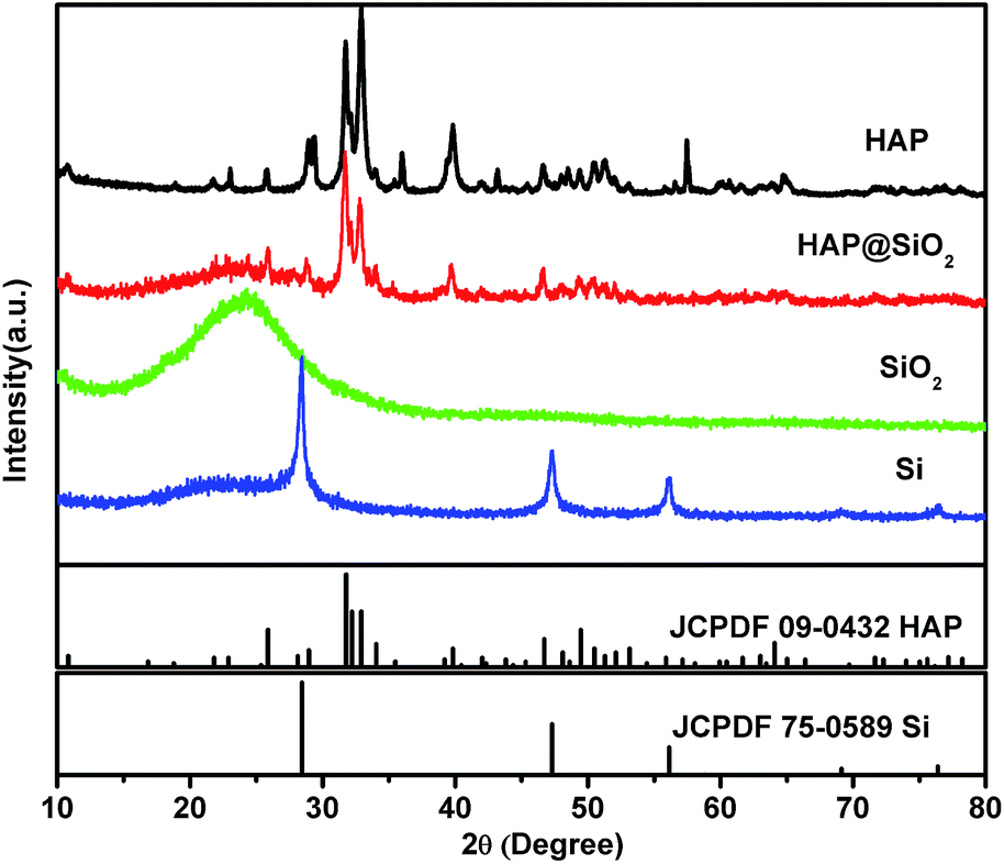 | ||
| Fig. 2 XRD patterns of HAP, HAP@SiO2, SiO2 and Si samples. | ||
 | ||
| Fig. 3 SEM images of (a) HAP, (b) HAP@SiO2, (c) SiO2 and (d) Si samples. | ||
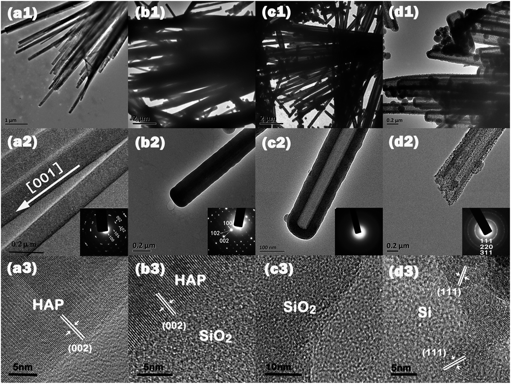 | ||
| Fig. 4 TEM, HREM images and SAED patterns of (a1)–(a3) HAP, (b1)–(b3) HAP@SiO2, (c1)–(c3) SiO2 and (d1)–(d3) Si samples. | ||
After magnesiothermic reduction, amorphous SiO2 was transformed to crystallized Si which shows sharp diffraction peaks that match well with the standard pattern (JCPDF card no. 75-0589) of cubic silicon (see Fig. 2). However, small amount of amorphous SiO2 was still detected suggesting incompleteness of the reaction, which is further indicated by chemical micro-analysis using EDS (see elemental line-scan in Fig. 3(d)).
The obtained Si NBs exhibit the same tubular morphology as SiO2 NBs, except the tube walls were constructed by aggregated Si nanoparticles in the size of several nanometers, resulting in the corrugated surface of Si NBs (Fig. 3(d)). Electron diffraction and high-resolution electron microscopy (HREM) clearly visualize high crystallinity of polycrystalline Si nanotubes (Fig. 4(d1)–(d3)).
The solid SiO2 powder was allowed to undergo the following reaction with Mg at a peak temperature of 650 °C.
| 2Mg (g, l) + SiO2 (s) → 2MgO (s) + Si (s) | (1) |
The starting composition that shows significant influences on both the purity and the morphology of the reaction product should be strictly controlled. After experimented with different proportion, we found that the optimal ratio of Mg and Si was 2:1. Less magnesium resulted in unreacted SiO2 locating among Si crystallites, which is supposed to worsen the Li+ transportation. Higher amount of magnesium could guarantee the fulfillment of reduction while in the meantime cause the formation of Mg2Si byproduct.
| 2Mg (g, l) + Si (s) → Mg2Si (s) | (2) |
The generation of Mg2Si has been found to promote coarsening of nano-grains, finally leading to fracture of the tubular structure. This happened due to the low alloy melting point and the high vapour pressure of Mg2Si.
Raman spectrum (see Fig. 5) of the Si NBs sample shows a sharp peak at 506.9 cm−1 which is assigned to crystallized silicon.33 The small broad peak at 940.2 cm−1 refers to the symmetric Si–O stretching vibrations.34 Therefore, all of the above structural and chemical characterizations indicate validity of the present synthetic method for crystalline Si nanotubes. It should be noted that no hazardous silane gas is applied in this high-yield method.
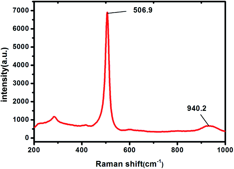 | ||
| Fig. 5 Raman spectrum of Si sample. | ||
Electrochemical cycling performances of Si NBs electrodes have been examined at 0.05 C (1 C = 4000 mA g−1) in coin-type half cells. For comparison, electrodes using Si nanoparticles have also been selected to measure the electrochemical properties. Si nanoparticles were synthesized by the same method of Si NBs without using HAP templates. They have the size of several nanometers and form agglomerates, which appear similar morphology of Si crystallites composed in Si NBs (see ESI†). The electrochemical cycling experiments indicated that Si NBs, in comparison with Si nanoparticles, exhibited a remarkable improvement in term of specific capacity and cycling stability. As it can be seen in Fig. 6(a), the first discharge and charge capacities for Si NBs electrode were 1497 and 933 mA h g−1, respectively. The coulombic efficiency was then evaluated to be ∼62%. For the Si nanoparticles, the first discharge and charge capacities were 1812 and 599 mA h g−1, respectively, and the coulombic efficiency was ∼33%. The Si nanoparticles electrode exhibited evident fading of discharge capacity (∼672 mA h g−1) in the second cycles i.e. a capacity loss as high as 63% compared with the first discharge capacity. In contrast, the Si NBs electrode displayed a much smaller decrease of capacity. Here, the Si NBs presented a capacity loss of only 44% and maintain a capacity of 833 mA h g−1 in the second cycle. In the following cycles, the capacity gradually decreased for both electrodes. The Si NBs achieved a relatively stable status within 10 cycles while the Si nanoparticles obtained a relatively stable status until after 40 cycles (see voltage profiles, Fig. 6(b) and (c)). The Si NBs maintained a stable capacity of ∼240 mA h g−1 after 50 cycles, which was almost fourfold the capacity (∼61 mA h g−1 after 50 cycles) of Si nanoparticle. These improvements could be ascribed to the tubular structure in Si NBs, which could provide enough space for alleviating the effect of volume change during cycling. Also, the bundle like structure could prevent the pulverization at the same time. Moreover, the tubular structure could help to form relatively stable solid electrolyte interphase (SEI) layers compared to Si nanoparticles, which could be convinced by cyclic voltammetry (CV) (Fig. 6(d) and (e)). The SEI layers could further hinder the tubular structure from fragmentation.35
 | ||
| Fig. 6 (a) Electrochemical cycling results for Si NBs electrode and Si nanoparticle electrode. (b) Voltage profiles plotted for the first, 2nd, 10th, 30th and 50th cycles for Si NBs electrode and (c) for Si nanoparticles electrode. (d) Cyclic voltammetry curves for Si NBs and (e) for Si nanoparticles anode. (f) The Nyquist plots for Si NBs electrode and Si nanoparticles electrode before cycling. | ||
CV was carried out to identify the characteristics of the redox reactions during charge/discharge cycles of Si NBs and Si nanoparticles anodes material (Fig. 6(d) and (e)). As can be seen in Fig. 6(d), the first cycle differs from those followed. It has been considered that the reduction peak at 0.6–0.8 V versus Li/Li+ corresponds to the formation of SEI layers on the surface of Si active materials.36 A sharp reduction peak around +0.1 V (vs. Li/Li+) on the charging curve indicating the Li-alloying process, see eqn (3). Two anodic peaks appeared at 0.3 and 0.6 V in the anode branches of CV curves were attributed to the de-alloying process of LixSi alloys, see eqn (4).37 The Si nanoparticle anode unfortunately did not form steady SEI layer at first cycle. From Fig. 6(e) we cannot see the reduction peak of SEI clearly; instead, the curve became a little apparent in the following cycles, suggesting an unsteady SEI formation process. This may explain the better cycling performance of Si NBs anode material than Si nanoparticle.
| Li alloy: Si + xLi → LixSi | (3) |
| Li de-alloy: SixLi → Si + xLi | (4) |
Fig. 6(f) shows the impedance spectroscopy of Si NBs electrode and Si nanoparticles electrode. For both electrodes, the Nyquist plots consist of an out-of-shaped semicircle alike in appearance of a half ellipse in high frequency ranges and an arc in low frequency range at the initial state. The arc might be attributed to the phase formation process in the low-frequency region. For both Si anodes, there were a phase transformation process from crystal-silicon to amorphous LixSi (0 < x ≤ 4.4).38 The out-of-shaped semicircle in the high frequency range carries information on the characteristics of the solid electrolyte interface (SEI).39 Compared to Si NBs electrode, Si nanoparticles electrode had a smaller semicircle, suggesting a smaller SEI resistance. Such discrepancy may be correlated to the phase purity of different nanomaterials. XRD patterns (see ESI, Fig. 3S†) of Si NBs and Si nanoparticles were both composed of diffraction peaks of crystalline Si and a broad peak characteristic of amorphous SiO2. It was worth to note that the intensity of broad peak from amorphous SiO2 in Si nanoparticles is slightly lower than that in Si NBs, indicative of smaller silica content in Si nanoparticles, hence smaller SEI resistance. Albeit this, the overall electronic performances of Si NBs were better than Si nanoparticles as anode materials. These results indicated that the better performance of Si NBs could be ascribed to the nanotube structure, which allows them to accommodate a large volume change during cycling.
Though the present work provides a feasible high-yield and safe synthetic method for Si NBs used as an electrode material in LIBs, it should be noted that both Si NBs and Si nanoparticles show a comparatively lower capacity than similar Si nanomaterials reported elsewhere. Via using similar magnesiothermic reduction synthetic method, the capacity of Si nanotubes reported by Chen's group and that of carbon-coated Si nanotubes developed by Kang’ group was about 1050 mA h g−1 (0.5 C) and around 900 mA h g−1 (0.1 C) after 90 cycles, respectively.40,41 These reported Si nanotubes showed thinner tube wall thickness as well as higher electrical conductivity. For porous Si fabricated via a similar magnesiothermic method, Wang et al. obtained a capacity of 376 mA h g−1 after 30 cycles at a current density of 0.2 mA cm−2 by using larger doses of Mg (molar ratio of Mg to Si about 2.5). However, the cycling stability was not as good as that in our present work, probably owing to their poor microstructure of the tubes.42 If such Si materials were coated with graphene, both the capacity and the cycling stability could be improved (633 mA h g−1). Therefore, the main reason for the lower capacity in our present work might be attributed to the larger SiO2 content as well as poor electrical conductivity of these silicon nanotube bundles. More efforts should be done to enhance reduction of SiO2 in magnesiothermic process. Meanwhile, coating with electrical conducting layer such as carbon-based components could be a promising strategy to improve electrical conductivity.
4. Conclusions
In summary, we reported a feasible method for high-yield synthesis of Si NBs based on magnesiothermic reduction kinetics. Nontoxic HAP nanobelt bundles were used as sacrificial templates to synthesize SiO2 NBs followed by a magnesiothermic reduction process to transform SiO2 NBs to Si NBs. The as-prepared Si NBs exhibit uniform size with ∼300 nm in external diameter, 80 nm in tube thickness and up to tens of micrometers in length. They are composed of silicon crystallites of around several nanometers. The Si NBs were then served as anode material in LIBs, which showed a reversible capacity of 240 mA h g−1 with little fading after 50 cycles. Such electrochemical performance is much better than electrodes using Si nanoparticles. We believe that Si NBs synthesized by the present method would be a promising candidate for high-performance anode material in advanced LIBs, provided that electrical conductivity and purity of silicon crystallites were further improved through, for instance, coating with carbon foil and tuning the magnesiothermic reduction conditions, respectively.Acknowledgements
This work was supported by National Natural Science Foundation of China (NSFC, no. 51272270, 61327811) and Innovation Program of SICCAS (Y37ZC4140G).Notes and references
- M. Armand and J. M. Tarascon, Nature, 2008, 451, 652–657 CrossRef CAS PubMed.
- J. M. Tarascon, Philos. Trans. R. Soc., A, 2010, 368, 3227–3241 CrossRef PubMed.
- B. Scrosati, J. Hassoun and Y.-K. Sun, Energy Environ. Sci., 2011, 4, 3287 CAS.
- Y. Yao, J. Zhang, L. Xue, T. Huang and A. Yu, J. Power Sources, 2011, 196, 10240–10243 CrossRef CAS PubMed.
- Z. Zhou, Y. Xu, M. Hojamberdiev, W. Liu and J. Wang, J. Alloys Compd., 2010, 507, 309–311 CrossRef CAS PubMed.
- J. Bae, J. Solid State Chem., 2011, 184, 1749–1755 CrossRef CAS PubMed.
- H. S. Kim, K. Y. Chung and B. W. Cho, J. Power Sources, 2009, 189, 108–113 CrossRef CAS PubMed.
- Y. Zhang, X. G. Zhang, H. L. Zhang, Z. G. Zhao, F. Li, C. Liu and H. M. Cheng, Electrochim. Acta, 2006, 51, 4994–5000 CrossRef CAS PubMed.
- S. Ohara, J. Suzuki, K. Sekine and T. Takamura, J. Power Sources, 2004, 136, 303–306 CrossRef CAS PubMed.
- H. J. Jung, M. Park, Y. G. Yoon, G. B. Kim and S. K. Joo, J. Power Sources, 2003, 115, 346–351 CrossRef CAS.
- D. Billaud, E. Mcrae and A. Herold, Mater. Res. Bull., 1979, 14, 857–864 CrossRef CAS.
- X. S. Zhou, A. M. Cao, L. J. Wan and Y. G. Guo, Nano Res., 2012, 5, 845–853 CrossRef CAS.
- M. H. Ryou, J. Kim, I. Lee, S. Kim, Y. K. Jeong, S. Hong, J. H. Ryu, T. S. Kim, J. K. Park, H. Lee and J. W. Choi, Adv. Mater., 2013, 25, 1571–1576 CrossRef CAS PubMed.
- T. H. Hwang, Y. M. Lee, B. S. Kong, J. S. Seo and J. W. Choi, Nano Lett., 2012, 12, 802–807 CrossRef CAS PubMed.
- R. C. de Guzman, J. H. Yang, M. Ming-Cheng, S. O. Salley and K. Y. S. Ng, J. Mater. Sci., 2013, 48, 4823–4833 CrossRef CAS.
- K. Karki, E. Epstein, J. H. Cho, Z. Jia, T. Li, S. T. Picraux, C. Wang and J. Cumings, Nano Lett., 2012, 12, 1392–1397 CrossRef CAS PubMed.
- C. K. Chan, H. L. Peng, G. Liu, K. McIlwrath, X. F. Zhang, R. A. Huggins and Y. Cui, Nat. Nanotechnol., 2008, 3, 31–35 CrossRef CAS PubMed.
- P. P. Fu, Y. J. Song, H. F. Zhang, H. B. Yang, Z. X. Zhou, M. T. Wu, L. H. Huang and G. Xu, Chin. J. Inorg. Chem., 2006, 22, 1823–1827 CAS.
- Z. H. Wen, G. H. Lu, S. Mao, H. Kim, S. M. Cui, K. H. Yu, X. K. Huang, P. T. Hurley, O. Mao and J. H. Chen, Electrochem. Commun., 2013, 29, 67–70 CrossRef CAS PubMed.
- X. Huang, J. Yang, S. Mao, J. Chang, P. B. Hallac, C. R. Fell, B. Metz, J. Jiang, P. T. Hurley and J. Chen, Adv. Mater., 2014, 26, 4326–4332 CrossRef CAS PubMed.
- Y. Zhou, X. Jiang, L. Chen, J. Yue, H. Xu, J. Yang and Y. Qian, Electrochim. Acta, 2014, 127, 252–258 CrossRef CAS PubMed.
- Y. Li, X.-Y. Yang, Y. Feng, Z.-Y. Yuan and B.-L. Su, Crit. Rev. Solid State Mater. Sci., 2012, 37, 1–74 CrossRef.
- R. O. Al-Kaysi, R. J. Dillon, L. Zhu and C. J. Bardeen, J. Colloid Interface Sci., 2008, 327, 102–107 CrossRef CAS PubMed.
- Y. Chen, X. Xue and T. Wang, Nanotechnology, 2005, 16, 1978–1982 CrossRef CAS.
- C. Gao, Q. Zhang, Z. Lu and Y. Yin, J. Am. Chem. Soc., 2011, 133, 19706–19709 CrossRef CAS PubMed.
- T. Homma, J. Komadina, Y. Nakano, T. Ouchi, T. Akiyoshi, Y. Iishibashi, Y. Nishimura, T. Nishida and Y. Fukunaka, ECS Trans., 2012, 41, 9–15 Search PubMed.
- Y. Chen, B. Li, X. Wu, X. Zhu, M. Suzuki, K. Hanabusa and Y. Yang, Chem. Commun., 2008, 4948–4950 RSC.
- C. Zhao, Q. Li, W. Wan, J. Li, J. Li, H. Zhou and D. Xu, J. Mater. Chem., 2012, 22, 12193 RSC.
- P. Qi, W. S. Wong, H. Zhao and D. Wang, Appl. Phys. Lett., 2008, 93, 163101 CrossRef PubMed.
- G. Yuan, H. Zhao, X. Liu, Z. S. Hasanali, Y. Zou, A. Levine and D. Wang, Angew. Chem., Int. Ed., 2009, 48, 9680–9684 CrossRef CAS PubMed.
- C. B. Gao, Z. D. Lu and Y. D. Yin, Langmuir, 2011, 27, 12201–12208 CrossRef CAS PubMed.
- Z. Bao, M. R. Weatherspoon, S. Shian, Y. Cai, P. D. Graham, S. M. Allan, G. Ahmad, M. B. Dickerson, B. C. Church, Z. Kang, H. W. Abernathy, 3rd, C. J. Summers, M. Liu and K. H. Sandhage, Nature, 2007, 446, 172–175 CrossRef CAS PubMed.
- N. H. Hai, I. Grigoriants and A. Gedanken, J. Phys. Chem. C, 2009, 113, 10521–10526 CAS.
- W. Chen, Z. L. Fan, A. Dhanabalan, C. H. Chen and C. L. Wang, J. Electrochem. Soc., 2011, 158, A1055–A1059 CrossRef CAS PubMed.
- H. Wu, G. Chan, J. W. Choi, I. Ryu, Y. Yao, M. T. McDowell, S. W. Lee, A. Jackson, Y. Yang, L. B. Hu and Y. Cui, Nat. Nanotechnol., 2012, 7, 309–314 Search PubMed.
- X. Xin, X. Y. Yao, Y. M. Zhang, Z. P. Liu and X. X. Xu, J. Solid State Electrochem., 2012, 16, 2733–2738 CrossRef CAS.
- T. Grunzel, Y. J. Lee, K. Kuepper and J. Bachmann, Beilstein J. Nanotechnol., 2013, 4, 655–664 CrossRef PubMed.
- E. Barsoukov, J. H. Kim, D. H. Kim, K. S. Hwang, C. O. Yoon and H. Lee, J. New Mater. Electrochem. Syst., 2000, 3, 303–310 Search PubMed.
- S. Zhou and D. W. Wang, ACS Nano, 2010, 4, 7014–7020 CrossRef CAS PubMed.
- Z. Wen, G. Lu, S. Mao, H. Kim, S. Cui, K. Yu, X. Huang, P. T. Hurley, O. Mao and J. Chen, Electrochem. Commun., 2013, 29, 67–70 CrossRef CAS PubMed.
- J. K. Yoo, J. Kim, Y. S. Jung and K. Kang, Adv. Mater., 2012, 24, 5452–5456 CrossRef CAS PubMed.
- L. Shen, X. Guo, X. Fang, Z. Wang and L. Chen, J. Power Sources, 2012, 213, 229–232 CrossRef CAS PubMed.
Footnote |
| † Electronic supplementary information (ESI) available: Preparation and characterization of Si nanoparticles, XRD comparison of Si NBs and Si nanoparticles. See DOI: 10.1039/c4ra05907g |
| This journal is © The Royal Society of Chemistry 2014 |