Juan Beltran-Huarac*a,
Javier Palominoa,
Oscar Restoa,
Jingzhou Wangb,
Wojciech M. Jadwisienczakb,
Brad R. Weinera and
Gerardo Morella
aDepartment of Physics and Department of Chemistry, University of Puerto Rico, San Juan, PR 00936, USA. E-mail: juan.beltran1@upr.edu
bSchool of Electrical Engineering and Computer Science, Ohio University, Athens, Ohio 45701, USA
First published on 18th August 2014
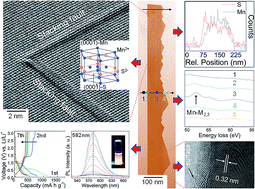
We report here a straightforward method to fabricate single-crystal wurtzite-structured manganese sulfide nanosaws (γ-MnS NSs) via a chemical vapor deposition technique, which can be extended to different types of binary chalcogenide-based 1D building blocks. Advanced spectroscopy and electron microscopy techniques were applied to reveal the structure, morphology and composition of these nanostructures. Our studies indicate that γ-MnS NSs are of high crystalline quality and purity, exhibit high aspect ratio and have extrusive teeth with average tip size of approximately a couple of atoms. These NSs are structurally stable and do not present divergence in surface energy. The formation of the backsaw is governed by a vapor–liquid–solid growth mechanism, whereas the teeth are a result of a self-catalyzed growth process induced by the Mn-terminated (0001) surface. Our optical and electrochemical analyses indicate that γ-MnS NSs can be used as efficient visible light emitters with an activation energy of ∼40 meV, and as anode materials with improved cycling stability for LIBs. This bottom-up approach represents a step ahead to provide promising and potential Mn-based materials for high-performance LIB technology and optoelectronics, and adds a new member to the family of saw-like wurtzite-structured nanoribbons, such as CdSe and ZnS.
Manganese sulfide (MnS) is a p-type semiconductor (Eg ∼ 3.2 eV at room temperature) and crystallizes in three distinct phases: rock-salt (α-MnS), zinc-blende (β-MnS) and wurtzite (γ-MnS).6 Metastable hexagonal bulk γ-MnS does not exist in nature, but its production in the laboratory under unusual conditions shows that γ-MnS exhibits unique chemical, electrical and magneto-optical properties superior to those of stable α-MnS.17,18 Currently, studies on the architectural control of nanostructured γ-MnS have revealed that these nanostructures present high photoluminescence, improved antiferromagnetic response, and high reversible capacity and cycling stability.6,19–23 Such advanced characteristics are expected to be exploited in improving the performance of optoelectronic devices, in developing new elements for diluted magnetic semiconductor (DMS) technology, and in implementing a novel anode material for Li-ion batteries (LIBs). Even though some reports on the synthesis of γ-MnS nanofibers have appeared in the literature,24–26 studies focused on the fabrication of γ-MnS have failed to produce single-crystal nanosaws, i.e., nanoribbons exhibiting one side flat and the other side saw-toothed. Their single-crystal nature are critical to avoid the grain boundary scattering present in polycrystalline MnS that affects the optoelectronic performance due to the high density of nanosized grains distributed across the surface. Also, their striking morphology would be crucial for any desired, potential and promising application.
In order to provide a new 1D building block based on MnS having a non-conventional cross-section, a higher surface-to-volume ratio (when compared to nanorods of MnS), and a highly-stable surface structure, we report here for the first time the fabrication of single-crystal wurtzite-type MnS nanosaws (NSs) via a chemical vapor deposition (CVD) route that is both inexpensive and environmentally-friendly. This particular morphology opens up the possibility of extending the scope of applications of γ-MnS, including: customized nanocantilevers for probing scanning technology, gas sensors, field-effect transistors, nanoresonators, photoconductive semiconductor switches, visible light emitters and anode materials for high-performance LIBs. In this regard, we also investigate the photoluminescence (PL) properties of γ-MnS NSs and evaluate their performance as an anode material for LIBs.
:
3 Mn/S molar ratio. MnCl2 was positioned in the middle of the furnace (hot zone), where the temperature (1273 ± 10 K) was monitored; while the sulfur (downstream) and the Si substrate (upstream) were placed at certain distances from the MnCl2 (170 and 115–100 mm, respectively) and kept at ∼673 K and 973–1123 K, respectively (see (ref. 6) for a depiction of the apparatus employed). The reaction tube was first evacuated for several hours down to 465 mPa to purge oxygen, heated to 1273 K, and filled to 46.5 Pa with a constant Ar flow at 20 sccm, which was used as carrying gas to transport the sublimated vapor to the cooler regions within the chamber for deposition. It was observed that after 1 h, the MnCl2 and S were fully consumed. After this, the tube was left to cool spontaneously to room temperature. In the absence of catalytic material, no γ-MnS NSs were obtained. The nanosaws were transferred to TEM grids upon carefully scratching the Si surface using a diamond tip for characterization and analyses.
:
DMC 1
:
1, v/v). All the electrochemical measurements were performed at room temperature using a Gamry Instruments potentiostat and PHE200 electrochemical software. The coin cells were tested in the potential window of 0.01–3.0 V vs. Li/Li+, and the applied current density was 200 mA cm−2. The ac impedance spectra were collected (after cell potential stabilization) by applying a sinusoidal signal with amplitude of 5.0 mV over the frequency range from 1 mHz to 100 kHz, and using EIS300 electrochemical software.
Similar findings were observed for (110) and (112) peaks of the diffractogram. The cubic β-MnS phase found is ascribed to the temperature gradient formed during the synthesis process, which is typical for MnS.6,24 Otherwise, the sharp peaks found and the absence of impurities in the XRD pattern indicate that the metastable γ-MnS phase is of high crystalline quality and purity.
The γ-MnS films were also studied by Raman scattering spectroscopy (Fig. 1b). The well-pronounced low-frequency Raman band observed was simulated using the damped harmonic oscillator phonon model (DHOPM).6,9 From the simulation, the Raman mode is determined to be at 592 cm−1, and can be ascribed to scattering involving two magnon branches (2M) occurring in MnS.25 The corresponding fit shows that this band is red-shifted by ∼23 cm−1 and narrow (FWHM ∼22 cm−1) when compared to bulk MnS,25 which is a clear indicator that the γ-MnS phase is under tensile stress developed during the growth process under CVD conditions. Note that this band is relatively weak owing to the fact that the Raman spectrum was collected at room temperature, which is above the Néel temperature (TN ∼ 90 K) for γ-MnS nanostructures.26 Taken altogether, the Raman analysis indicates the formation of MnS with wurtzite structure, consistent with the XRD analysis.
The FE-SEM images of γ-MnS taken at different magnifications are depicted in Fig. 2. The average thickness of γ-MnS films was found to be ∼25 μm (see Fig. 2a and inset therein). These films present a densely populated surface with spaghetti-like NRs, with the catalytic material on the ends thereof (see Fig. 2b and inset therein), indicating that they grew following a catalyst-based mechanism. It was also found that γ-MnS NRs possess a high aspect ratio (AR) with widths falling in the range of 100–350 nm and lengths over 25 μm. Fig. 2c and d show that the majority of the NRs observed are comb-shaped, i.e., NRs with one side flat and the other side saw-toothed. These NRs exhibiting this particular cross-section will be referred to from now on as NSs. Similar morphologies were recently reported by Ma et al. working on wurtzite ZnS and CdSe nanostructures.27,28 γ-MnS NBs are also present in the as-grown samples, but they are not the dominant component. Extensive electron microscopy observations suggest that both saw- and belt-like nanostructures, (which were obtained in the same growth temperature range) possess a common nucleation site,27 indicating that they are nucleated and grown as bunches randomly dispersed on the substrate.
![]() | ||
| Fig. 2 (a–d) FE-SEM images of γ-MnS NSs. Inset in (a) shows a low-magnification FE-SEM image of the product. Insets in (b) and (d) show the catalytic and a close-up of an individual NS, respectively. | ||
The HRTEM image depicted in Fig. 3a shows that the geometrical shape of the γ-MnS nanostructures is belt-like with uniform width along their length and widths in the range of 80 to 250 nm. Catalytic particles were observed on the ends of the NBs, evidencing that the vapor–liquid–solid (VLS) process is the prevailing growth mechanism. The ripple-like contrast seen in inset of Fig. 3a is most likely a result of the strain generated from the bending of the belt, since the degree of flexibility of the NBs is associated to their thickness. However, it could also be related to the formation of stacking faults and twining occurring as a mechanism to stabilize the growth of the nanostructures. It was also observed that various NBs grow from a single nucleation site, which is consistent with the SEM analysis. Statistical analyses of the HRTEM images reveal that the dominant morphology in the products is saw-like, such as that depicted in Fig. 3b. Individual γ-MnS NSs consist of one flat side and one side with extrusive teeth, which resemble parallel triangles (∼10–50 nm high) grown along the NSs axes, similar to perfectly aligned nanocantilever arrays used in probing scanning technology. It was found that the ends (tips) of the cantilevers are atomically rough, as pointed out by the black arrowhead in the middle inset of Fig. 3b. The surfaces of the NSs were clean, smooth, and atomically resolved (see left upper inset of Fig. 3b, that corresponds to the rotated green-delineated selected area in Fig. 3b). Hence, this method provides an efficient route to develop 1D building blocks without any sheathed amorphous phase, having low degree of interdiffusion between the material itself and the surrounding medium. An inner view into the nanostructures (see lower and left upper insets of Fig. 3b) and the selected area electron diffraction (SAED, operated in TEM mode) analysis (see right upper inset of Fig. 3b corresponding to the selected area of left upper inset of Fig. 3b) evidence that: NSs grow along the [01
0] with top and bottom surfaces ±(2![[1 with combining macron]](https://www.rsc.org/images/entities/char_0031_0304.gif)
0), and side surfaces (0001); the growth direction of the NSs teeth is along [0001] with an interplanar spacing of 0.32 nm; and they are single crystal with wurtzite structure.
In order to clearly establish the elemental composition of the products, we have conducted energy-dispersive X-ray spectroscopy (EDS) and electron energy loss spectroscopy (EELS) measurements on individual γ-MnS NSs. Both techniques were operated in STEM mode. The EDS line-scans depicted in Fig. 4b (carried out on the region shown in Fig. 4a) show that the nanostructures consist of Mn and S with a molar ratio of ∼1
:
1. The width obtained by this technique (∼150 nm) correlates well with the values range estimated from the HRTEM analysis. The EDS elemental mappings (not shown here) revealed the overall distribution of Mn and S in the nanostructures. Line-scanned EELS spectra are depicted in Fig. 4c, which were carried out on the region shown in Fig. 4a. The EELS spectra show a band peaking at ∼55 eV, which corresponds to the low-loss Mn M2,3 transition.6 The spectra indicate that Mn fades at the teeth of the NSs, which is expected given that they are thinner than the backsaw (see next Section). The EELS probe used in this study was not adequate enough to resolve the light S atoms. However, a very weak signal was detected centered at ∼165 eV, which is attributed to the S L2,3 transition. Considered altogether, our findings show that single-crystal γ-MnS NSs were successfully synthesized by this method.
![]() | ||
| Fig. 4 (a) HRTEM image of an individual γ-MnS Ns. (b and c) EDS profile and ELLS spectra line-scanned from the region shown in (a). Inset in (c) shows the S L2,3-shell edge of γ-MnS. | ||
In order to gain more insight on the uniformity of the cross-sectional thickness, width of tip, and dislocations or defects present in γ-MnS NSs, we have carefully examined several NSs by illuminating them with 200 kV electrons for a somewhat longer time, but not enough to cause any increase of planar induced defects, damage, phase transformation or amorphous carbon deposition during the exposure. A representative HRTEM image of an individual NS is depicted in Fig. 5A. As noted, the NS is transparent to the TEM grid, which suggests that it is a few tens of nanometers thick. In fact, the backsaw thickness resulted to be in the range of 30 to 50 nm (see Fig. 5B and inset therein), and width-to-thickness ratios of ∼3.3 to 7.0. Interestingly, it was observed that the thickness was significantly reduced from the end of backsaw to the teeth (radially), reaching values as low as few nanometers. In this region, the NS (surface encompassed by the teeth) is structurally uniform and highly crystalline with two growth directions: [01
0] and [0001]. In addition, no dislocations were found, but rather single atomic-thick stacking faults along the NS and teeth axes (see Fig. 5C and F). A closer view into the tip of teeth shows that its surface is seamless having a wurtzite structure (according to the fast Fourier transform (FFT) indexation), and its width is approximately a couple of atoms thick (see Fig. 5D and F). A unit-cell model for the hexagonal phase of MnS is shown in the inset of Fig. 5C. It was observed that the projected position of the Mn atoms in the unit cell correlates well with the TEM projection image taken on the end of tip and oriented along (2![[1 with combining macron]](https://www.rsc.org/images/entities/char_0031_0304.gif)
0). The light sulfur atoms were less resolved by the TEM probe. Thus, the asymmetric growth behavior of the NR is ascribed to the polarization of the c-plane, which can be plausibly explained as follows: it is known that the chalcogen polar surfaces in chalcogenides and oxides (wurtzite ZnS, CdSe and ZnO) are unreactive,16,28,29 and (0001)-Zn and -Cd-terminated surfaces are chemically reactive, specifically to adsorb methanol, formaldehyde and formic acid, and ZnS and CdSe vapors. It was found that these active surfaces are responsible for growing saw-like structures (such as one- and double-sized NSs), acting as the self-catalyst.16,28,29 Thus, polar surfaces induce directly the formation of asymmetric NRs. It is reasonable to claim that the saw-like nature of wurtzite-structured MnS consisting of alternating layers of oppositely charged ions ((0001)-Mn2+ and (000
)-S2−) and stacked parallel to the c-axis is induced by both the surface polarization and surface termination (see inset of Fig. 5C). Even though this ionic crystal composed of tetrahedrally-coordinated Mn2+ and S2− layers exhibits an accumulating normal dipole moment (as a result of the surface polarization), γ-MnS NSs are shown to be stable without facets or massive surface reconstructions.
Taken altogether, the results indicate that single-crystal NSs were grown in two stages, as follows. First, the NRs are rapidly formed along [01
0] with top and bottom surfaces ±(2![[1 with combining macron]](https://www.rsc.org/images/entities/char_0031_0304.gif)
0), and side surfaces (0001), following a bottom-up Au-catalyst-based approach described by the VLS growth mechanism (see SEM analysis). Second, the subsequent growth (self-catalyzed from the Mn-terminated surface) of the teeth is conducted and oriented along [0001], which is a consequence of the surface polarization and surface termination of the wurtzite structure (see HRTEM analysis).
We have evaluated the temperature-dependent PL properties of these NSs on Si substrate in order to provide further insight into their structural properties on a macroscopic scale, and evaluate their potential applicability as visible light emitters. The PL spectra of γ-MnS NSs recorded between T = 10 to 300 K are depicted in Fig. 6a. An optical image of γ-MnS NSs suspended in aqueous solution as viewed under UV light excitation at 300 K is shown in the lower inset of Fig. 6a. The PL spectra at 300 K show one predominant yellowish-orange emission band peaking at ∼578 nm at, which is most likely ascribed to the optically radiative recombination of electrons in shallow traps of surface localized states and photogenerated holes caused by stacking faults found in the NSs.30–32 A relatively weak near band edge emission band centered at ∼371 nm and a defect-related emission band at 430 nm were observed at shorter wavelengths (see Fig. S1†). The near band edge emission of NSs is blueshifted ∼16 nm when compared to the bulk value (387 nm).19 This shift is due possibly to the tiny width (a couple of atoms thick) of the γ-MnS NSs tips, which give rise to a quantum confinement effect. Similar results were reported for CdSe NSs.28 However, another factor that may contribute to this blueshift is related to the small thickness of the NSs backsaws. The origin of the defect-related emission at 430 nm is presumably ascribed to the higher level transition of γ-MnS from the surface defects;22,33 however, further research is needed to confirm such presumption. The PL intensity of the surface defect-induced emission at 582 nm is four orders of magnitude stronger than the exciton-related emission band at 371 nm. This confirms the presence of high density of single stacking faults in the NSs, which is consistent with the HRTEM analysis. As the temperature decreases (down to 60 K), the yellowish-orange emission band experiences a redshift of ∼4 nm, which is ascribed to its shallow-trap emission character (see upper inset of Fig. 6a). No substantial shift was detected below 60 K. Fig. 6b shows that the yellowish-orange emission band experiences a remarkable drop in PL intensity as the temperature decreases, as expected. A relatively small change in PL intensity was observed over the temperature range from 300 to 180 K. A significant increase in PL intensity was observed at lower temperatures. The integrated PL intensity was doubled from 100 to 10 K, which corresponds to the carrier transfer from electrons trapped in the donor states that are promoted towards the conduction band. It is assumed that the interaction between neighboring Mn2+ ions also contributes to the carrier transfer, which is influenced by the antiferromagnetic spin-ordering given that more prominent PL intensity changes were observed below 100 K (TN ∼ 90 K).26,34 To determine the position of the donor level with respect to the conduction band, the experimental data were simulated through a thermally activated carrier-transfer model35 via
![]() | (1) |
![]() | ||
| Fig. 6 (a) Temperature-dependent PL spectra of γ-MnS/Si films excited with a 325 nm He–Cd pulse laser. The redshift of the yellowish-orange emission band is shown in the upper inset. The lower inset shows the optical image of γ-MnS NSs dispersed in aqueous solution as viewed under UV light at 300 K. (b) Emission band intensity evolution as a function of temperature fitted to eqn (1). Inset in (b) shows the PL decay curve fitted with a bi-exponential function. | ||
As an example of the versatility of these nanostructures, we have evaluated their electrochemical properties as a potential and alternative anode material for LIBs. These experiments were motivated by the atomically defined morphology, highly stable structure and high degree of crystallinity that the nanostructures present, which play key roles in electrochemical energy storage. Other factors that influenced the use of MnS as an anode material were the great abundance and low cost of Mn and S, and the fact that MnS exhibits a theoretical specific capacity (616 mA h g−1) higher than that of graphite (372 mA h g−1), and possesses a high lithium storage capacity.6 However, wurtzite-structured MnS as an anode material has been overlooked to date.
Charge–discharge experiments were carried out in coin cells, in the potential window of 0.01–3.0 V vs. Li/Li+ and current density of 200 mA g−1. The charge–discharge curves obtained are depicted in Fig. 7a. It was found that the initial specific discharge capacity and the corresponding charge capacity exceeded 1150 and 710 mA h g−1, respectively. These values were found to be higher than those of bulk MnS, which is related to additional capacity resulting from reversible reactions that occur between displaced Mn and the electrolyte solvents.39 The irreversible capacity loss (38%) is due presumably to the electrolyte decomposition, which would give rise to the subsequent formation of solid-electrolyte interphase (SEI) layers on the electrodes surface. Such SEI formation is common for most MnS anode materials.40,41 A plateau was also observed at ∼0.5 V, which can be assigned to both carbon black additives and SEI layers. The extended flatness of this initial discharge voltage plateau is attributed to the superior crystallinity, stable surface site energetics, and larger electrochemical active surface area of γ-MnS NSs. From the second cycle onwards, this plateau vanishes almost completely signifying that the formation of the SEI layer takes place predominantly during the first cycle. The discharge capacity obtained in the second cycle was 780 mA h g−1, representing a notable cyclic capacity retention ∼70%, being reduced up to 50% at the third cycle (530 mA h g−1), from which point on small and regular changes were observed. This result is interesting given that the initial capacity of commercial MnS falls off severely over cycling.40 In general, metal sulfides do not exhibit good charge cycling stability. Our results suggest that γ-MnS NWs show improved cycling with an increasing Coulombic efficiency of 96% in the second cycle, and retain a stable reversible capacity of ∼200 mA h g−1 after 40 cycles (see inset of Fig. 7a).
A rapid derivative of the capacity with respect to cell potential reveals three reduction peaks in the cathodic region: the peak at ∼0.01 V represents the lithiation of carbon;42 the peak at ∼0.2 V is associated to the formation of Mn and Li2S (see eqn (3)), or to the non-aqueous electrolyte decomposition during the discharge process;40 and the peak at ∼0.7 V is certainly attributed to the insertion of lithium into γ-MnS NSs structures to form a homogeneous phase of Li2MnS (see eqn (1)). Similarly, two oxidation zones are observed in the anodic region: the zone between 0.15–0.35 V corresponds to deintercalation of lithium stored in the carbon black;42 and the zone between 0.6–1.3 V is ascribed to the extraction of lithium from γ-MnS.40,43 These observations indicate that the SEI layer is thin and stable having high ionic conductivity, and the electrochemical reversible reactions in the MnS anode during the charge–discharge processes can be described by a two-stage lithiation mechanism as follows:40,44
| MnS + 2Li+ + 2e− ↔ Li2MnS | (2) |
| Li2MnS + 2e− ↔ Mn + Li2S | (3) |
To further investigate the interface reaction between the electrolyte solution and the anode electrode, we have conducted ac impedance measurements carried out at an open circuit potential of 0.6 V in the 23rd charge cycle. Nyquist plots depicted in Fig. 7b show two overlapping high-to-medium frequency semicircles. The higher-frequency one is attributed both to the SEI layer at the active material/electrolyte interface and to the contact resistance, while the medium-frequency one corresponds to the charge transfer resistance on the electrode/electrolyte interface.39,41 The spectrum in the low-frequency range is associated to synergistic resistive effects and to the Li-ions diffusion into the active material (Warburg resistance). The same results were obtained after 40 cycles suggesting that the anode material shows a good electrical contact between the active material and the current collector, and exhibits a good structural stability. These results can be summarized upon fitting the spectra of the cells and representing them as a first approximation by an equivalent circuit, as shown in inset of Fig. 7b, where Rsol is the electrolyte resistance, CPE is the constant phase element, Rlr is the surface layer-related resistance, Cdl is the double layer capacitance, Rct is the charge transfer resistance at the interface and W is the Warburg element. It was also found that the diameters of the semicircles are relatively smaller than those of hollow cubic MnS microspheres and MnS nanoparticles.39,41 This further evidences that γ-MnS electrode exhibits high electrical conductivity, which would induce in turn a rapid electron transport during the lithium insertion/extraction reaction and would enhance the reversible capacity.
Taken altogether, we suspect that the diffusion of Li+ ions towards the exposed teeth of MnS NSs provides abundant surface area for lithium diffusion through the interatomic spacing, and subsequent intercalations into different layers of the active material. As a result, a significant volumetric expansion (which is efficiently accommodated) and weak amorphization process (see inset of Fig. 7b) take place. Moreover, the structural flexibility of the NSs facilitates the prevention of detachment and agglomeration processes, thus allowing a more effective Li/electron diffusion during charge–discharge cycles. The improved cyclic capacity retention can be also assigned to the high degree of crystallinity, single-crystal architecture and structural integrity of these nanostructures, which offer transport advantages for both charge carriers.
0] and [0001] directions and their surfaces are defined by unambiguous crystallographic planes. The asymmetric growth behavior is probably induced by the polarization of the c-plane, being the surface polarity a critical parameter to control the morphology of the nanostructures. This method employs MnCl2 and sulfur powder as starting materials instead of commercial γ-MnS powder, which would significantly reduce the production costs of γ-MnS and circumvent difficulties related to stoichiometry retention of γ-MnS powder on the desired substrates during deposition process. These structurally uniform and geometrically perfect NSs are promising to be used as nanocantilever arrays for nanosensors and nanotweezers. This breakthrough advances novel methods to fabricate 1D building blocks suitable for optoelectronics and Li-ion battery applications.
Footnote |
| † Electronic supplementary information (ESI) available: The near band edge and surface defect related emissions bands at 300 K of γ-MnS/Si films excited with a 325 nm He–Cd laser. See DOI: 10.1039/c4ra05561f |
| This journal is © The Royal Society of Chemistry 2014 |