Going beyond the self-assembled monolayer: metal intercalated dithiol multilayers and their conductance

Hicham Hamoudi*a, Kohei Uosakia, Katsuhiko Arigaa and Vladimir A. Esaulovb
aInternational Center for Materials Nanoarchitectonics (WPI-MANA), National Institute for Materials Science (NIMS), 1-1 Namiki, Tsukuba, 305-0044, Japan. E-mail: HAMOUDI.Hicham@nims.go; Fax: +81-29-860-4706; Tel: +81-29-851-3354 ext. 8672
bInstitut des Sciences Moléculaires d'Orsay, Unité mixte de Recherche CNRS-Université Paris Sud, UMR 8214, Université Paris Sud, bât. 351, Orsay 91405, France

Received 9th June 2014 , Accepted 18th August 2014

First published on 20th August 2014


Abstract

A study of the self-assembly of silver atom intercalated 5,5′-bis(mercaptomethyl)-2,2′-bipyridine (BPD; HS-CH2-(C5H3N)2-CH2-SH) and 1,4-benzenedimethanethiol (BDMT; HS-CH2-(C6H4)-CH2-SH)) dithiol (DT) multilayers on gold is presented. The bilayer of these SAMs can be obtained starting from the exposure of a DT monolayer to a concentrated silver ion solution. After grafting the silver atoms on the sulfur end group, the incubation of the resulting DT–Ag SAM in a DT solution leads to the formation of a DT–Ag–DT bilayer. This process was extended to make a multilayer structure. The corresponding changes in these self-assembled layers on Au are characterized by X-ray photoelectron spectroscopy (XPS), spectroscopic ellipsometry (SE) measurements, and IV characteristics. Our interpretation of evolution in the absorbed layer are based on changes in intensities of peaks in XPS related to S bound to substrate or Ag and in –SH groups, as well as changes in thickness and absorption features in SE measurements. The latter show the evolution in absorbance wavelength as a function of thickness and indicate a decrease in the HOMO–LUMO gap from about 4.5 eV to 4 eV. The IV characteristics show a significant bias dependence on the number of the BPD layers and there appears to be a transition from tunneling to a hopping regime when going from the single to the multiple layers.

Introduction

In this paper we address the question of step by step building up of organic–metal–organic heterostructures. Metallization of organic layers1,2 is a subject of longstanding interest and many applications can be found in every-day-life. This subject has attracted much attention recently because of interest in organic electronics, light emitting diodes, sensors and in general in relation with adhesion of bio-molecules to surfaces, with e.g. applications in biology and medicine. A step beyond this is the building up of more complex organic–metal–organic scaffolds.

The basic building block in our work is a dithiol molecule, which provides the possibility of using the two-thiol terminations to bind to different metallic entities.1–6 Thus in some earlier works e.g. pentanedithiol molecules were used4 to first assemble a SAM on a metal surface from ethanolic solutions, then deposit on them metal nanoparticles and finally upon these graft further pentanedithiols. Similar attempts have been made by various groups and by some of us47–50 e.g. using 1,4-benzenedimethanethiol (BDMT) and hexanedithiol SAMs prepared in ethanolic solutions, with solution deposition of metal atoms on the SAM.

It should be noted that interest in molecules with phenyl units is related to the fact that they have better conducting properties and are better adapted as molecular contacts between nanosized metallic electrodes.7–18 Indeed, the first conduction measurements on molecules involved measuring the resistance of a 1,4-benzenedimethanethiol (BDMT) molecule.19 This was performed using a scanning tunneling microscopy (STM) tip held on a gold nanoparticle deposited on top of a BDMT SAM. Thus the case of BDMT molecules presented a particular interest for these studies. It is worth noting here that generally molecules do not behave as simple ohmic conductors and have non-linear current–voltage characteristics. The problem of conductivity in molecular wires have been a subject of different investigations.41,42 Recently the electrical resistance of oligophenyleneimine (OPI) molecules of various lengths have been investigated using a conductive AFM tip.42 Hopping transport was found in longer OPI molecules, while the small molecules in length exhibited coherent transport. Similar results have been reported using the Fe(II)-bis(terpyridine) molecular system.41

In practice, the formation a highly ordered compact SAMs, with free –SH end groups at the outer interface, depends on various factors such as the quality of the substrate and reagents, solvent strength, photochemical action, and so on, and has been, and is still debated. Thus for instance, solution formation of small length alkane SAMs, like the pentanedithiol and hexanedithiol SAM mentioned above,4,7 is known to be problematic and frequently leads to mainly lying down molecules.20–22 Similarly we have observed previously23,24 that assembly of BDMT in ethanolic solutions as used in ref. 12 is problematic and can lead to disordered layers. Thus the first step in building such organic metal–organic heterostructures requires the establishment of robust standing up ordered dithiol SAM formation protocols. We recently investigated assembly of several alkanedithiol and also BDMT dithiol molecules20–27 using a combination of different techniques. SAMs based on BDMT grown on noble metals from solution were chosen as a good prototype system for the study of aromatic dithiol assembly (DT). The assembly of these molecules shows a better stability compared to saturated molecules because of the lateral interactions between the aromatic rings of adjacent molecules. We found previously that dithiol SAMs with aromatic units are better ordered than the ones with CH2 groups.21–24 A well reproducible protocol, allowing formation of well-ordered BDMT SAMs from degassed n-hexane solutions, in the absence of light, was established23,24,50 and the SAMs characterized by high resolution XPS, NEXAFS, RAIRS and spectroscopic ellipsometry (SE). These studies thus showed formation of an ordered SAM with standing up DT molecules inclined at 24° to the normal.

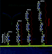
Layer by layer assembly starting from a SAM, has attracted much interest5,51 and different approaches depending upon molecule type have been attempted.52–54 Here we ask ourselves the question whether it is indeed possible to build a multilayer SAM starting from the highly quality dithiol SAM? We base ourselves on the results of these earlier works,23,24,50 and have used a combination of SE, and XPS to study the formation of the bilayer of BDMT and also 5,5′-bis(mercaptomethyl)-2,2′-bipyridine (BPD) self-assembled films on Au, with intercalated Ag atoms. In the following we refer to these generically as DT (dithiols). As shall be described below, first a DT SAM has been prepared using our established protocol. Then silver atoms were grafted to the SH end groups in a silver nitrate solution. We thus obtained a platform for further deposition of DT leading to a DT–Ag–DT bilayer on gold as schematized in Fig. 1. This process is further repeated to obtain longer molecular chains of up to four DT units. The conduction through these was then investigated to study differences as a function of chain length and strong differences were found when going from a SAM to the multilayers. In the following we shall refer to these scaffolds by the number of DT units as DTn (or BPDn).


image file: c4ra05476h-f1.tif
Fig. 1 Schematics of the method to prepare a BPD–Ag–BPD layer, we use in this paper.

Experimental section

BDMT (98% purity) and BPD (96% purity) were purchased from Aldrich and used as received. The gold substrates were prepared by thermal evaporation of 150 nm of gold (99.99% purity) onto either polished single-crystal silicon (100) wafers primed with a 10 nm titanium adhesion layer or on freshly cleaved mica at 340 °C. The DT SAM was prepared by immersing the gold support into a freshly prepared 1 mM solution of n-hexane. We used solutions well-degassed by Ar, and all preparation steps were performed, following the same protocol as in our previous studies.20,23 After that the gold wafer, modified with a layer of DT, was held in contact with 10 mM of AgNO3 for 10 min at ∼60 °C. Finally the resulting DT–Ag SAM was incubated in the DT solution as in the first step to yield the DT–Ag–DT bilayer. This procedure was extended to yield tri and quad layer Ag intercalated DT SAMs.

XPS spectroscopy measurements were conducted at the MANA Foundry using the XPS Thermo Fisher (Alpha 110 mm Analyser Sigma XPS version). The XPS spectra were recorded in the Au 4f, S 2p, and C 1s, and N 1s regions. The spectra acquisition was performed in normal emission geometry using the Al Kα radiation. The binding energy (BE) scale of each spectrum was individually calibrated to the Au 4f7/2 emission at 83.95 eV.

SE measurements were performed in the MANA Foundry on a recently upgraded rotating compensator spectroscopic ellipsometer (M-2000, J.A. Woollam Co. Inc.). The experimental protocol adopted for SE measurements on ultrathin layers has been thoroughly described in recent articles on thiolate SAMs on gold.28–30 The rather small spectral variations induced by the formation of nanometer thick layers are best seen by calculating the difference between the data for pristine and SAM covered substrates (δΨ = ΨfilmΨAu, δΔ = ΔfilmΔAu), for several zones of each sample. In this work spectra have been collected at 65° and 70° angles of incidence. The spot size on the sample was of the order of a few square millimeters. Measurements were performed ex situ, in laboratory atmosphere, immediately after extraction from solution and adequate rinsing.

The mono and the multilayers junctions were electrically tested on a probe station using a semiconductor parameter analyzer (Keithley Instruments Inc.) at room temperature and under vacuum to avoid the influence of water.

Results

XPS measurements

The SAM for BDMT/Au and BPD/Au were investigated by XPS. Here we will focus on the BPD based system, while some BDMT based data is given in the ESI (Fig. S1–S3). Fig. 2a shows the S 2p and the C 1s peaks regions of a BPD–Au sample, which was prepared by immersing in a freshly prepared, degassed, 1 mM solution of n-hexane for 1 h at ∼60 °C.
image file: c4ra05476h-f2.tif
Fig. 2 S 2p, C 1s and N 1s XPS spectra of BPD, BPD–Ag, and BPD–Ag–BPD.

The C 1s spectra of the BPD, are presented in Fig. 2b, with a decomposition into two components. The main peak at about 284.9 eV of the BPD SAM is a superposition of contributions from: the C–C moieties, and the C[double bond, length as m-dash]C in the ring unit,24,31 while the 285.6 eV peak is assigned to C–N.

The S(2p) spectra are decomposed into two components: two doublets with a fine structure splitting of 1.18 eV corresponding to S atoms bound to gold (SAu at 162 eV) and “free” SH atoms on top of the BPD SAM (at 163.5 eV). The initial BPD spectrum resembles the one measured for BDMT here (Fig. S1) and reported previously,23 but has different relative intensities of the SAu and S components. We recall that the SAu component appears with a lower intensity, because of attenuation of intensity of electrons passing through the organic layer.23,24 Because the BPD molecules are longer they result in a greater attenuation of electrons passing through the thicker layer and the SAu intensity is lower than for BDMT. We shall return to this point later.

Oxygen-coordinated sulfur species are practically absent since no peaks with S (2p3/2) binding energies above 168 eV are detected. The N 1s XPS spectra of the BPD SAM are displayed in Fig. 3. A single symmetric peak at 399 eV is observed and assigned to the nitrogen in the pyridine rings.


image file: c4ra05476h-f3.tif
Fig. 3 Ag 3d XPS spectra of the BPD–Ag and BPD–Ag–BPD layers.

Upon immersion of the DT SAM on Au, into the AgNO3 solution the ratio of the SAu and SH components changes and the SAu component increases significantly after exposure to Ag, as shown for the BPD case in Fig. 2a. We ascribe this to binding of Ag atoms to the top sulfur SH atoms, thus leading to a shift to lower core level binding energies, corresponding to binding to Ag, that is similar to the Au one.32 This results in the increase of the SAu peak intensity. In the present experiments, a small amount of the 163 eV S component remained.

The XPS investigation shows that Ag is indeed attached to the SAM, since we observe (Fig. 3) peaks at 368 eV and 373.9 eV, corresponding to the Ag 3d3/2 and Ag 3d5/2.32 This Ag spectrum appears quite symmetric and thus suggests a metallic nature of the deposit.32

The Ag–DT SAMs on Au were re-immersed into the n-hexane DT solution using the same protocol. The resulting XPS spectrum is shown in Fig. 2a for BPD. In this case we see a re-increase of the “free” S component, which we ascribe to binding of BPD molecules on top of the Ag–BPD SAM, and the resulting layer thus has free sulfur on top. Again the oxidized S structure appears to be quite small.

The total integrated intensity of the SAu and SH related peaks of the BPD, BPD–Ag and BPD–Ag–BPD SAM is shown in Fig. 4. One can clearly see here the decrease in the SH component for the BPD–Ag SAM and its re-increase in case of the BPD–Ag–BPD layer.


image file: c4ra05476h-f4.tif
Fig. 4 The intensity ratio S 2p to Au 4f for the BPD, BPD–Ag and BPD–Ag–BPD layers.

The Ag 3d peak intensity now decreases in the case of the BPD–Ag–BPD SAM, because of the screening of Ag by the BPD molecules attached to the Ag atoms on top of the BPD–Ag SAM (see Fig. 3).

We also observed (Fig. 2c) that the N (1s) intensity decreased for the BPD–Ag case, as could be expected because of additional Ag induced screening and then increased again for the BPD–Ag–BPD case, because of appearance of the second BPD layer.

The XPS data were additionally used to determine the effective thickness of the different SAMs (DT–Ag, and DT–Ag–DT). This was done on the basis of the Au 4f intensity, assuming a standard exponential attenuation of the photoelectron signal and using the attenuation lengths reported in ref. 31. Calculating the film thickness from the C 1s and Au 4f signals values of ∼1.95 and ∼4.1 nm are obtained for BPD–Ag and BPD–Ag–BPD, respectively.

A more detailed analysis of changes in the S 2p XPS spectral shapes and some comments about intensity changes shown above are discussed in greater length in a following section.

Spectroscopic ellipsometry

SE measurements were performed on the various layers studied. Results for BDMT SAM are given in the ESI (Fig. S4). Data for BPD are shown in Fig. 5a and b. For comparison we also performed measurements for an octadecane thiol (C18). The data are shown in the 245–1000 nm range for a 65° angle of incidence. The shapes of BPD δΨ and δΔ spectra resemble the ones for BDMT measured here and reported previously23 using the same preparation method. The δΨ BPD curve shows a dip for wavelengths less than 350 nm (minimum around 275 nm), a behavior similar to the BDMT case, for which it was previously23 assigned to absorption, related to aromatic rings, eventually influenced by intermolecular interactions in the SAM.23 We performed a measurement of absorption on a sample of BPD solution in water (in which BPD is more easily soluble than in hexane), which indeed shows absorption below 325 nm wavelength range (first peak at 293 nm; see inset in Fig. 5). Given solvent related shifts in absorption features and the fact that we deal with a SAM we believe our interpretation is reasonable.
image file: c4ra05476h-f5.tif
Fig. 5 SE measurements for the BPD, BPD–Ag, BPD–Ag–BPD and BPD4 layers: (a) δΨ and (b) δΔ. Note that the BPD4 data refers to the scale at the right. Data for C18 SH SAM is shown for comparison.

We also observe, as reported earlier for thiolate SAMs and BDMT, that for wavelengths above about 550 nm, the δΨ curve has a negative value. This phenomenon has been interpreted as due to the formation of a strong molecule–surface bond, leading to charge redistribution and chemisorption-induced structural and morphological changes which affect the mean free path of electrons.23,28,30

A comparison of the δΨ and δΔ spectra for the BDMT and BPD SAMs shows larger positive and negative values of δΨ and δΔ respectively for the BPD case in agreement with the longer length of the BPD molecule ∼2 nm. These data are directly compared with δΔ spectra obtained for C18 SAMs deposited under the same conditions of substrate preparation and incubation in order to estimate the thickness of the layer. The results for C18 are compatible with earlier work.29,30 We see that the results for the C18 SAM and BPD–Ag SAM are fairly close, indicating that they have similar thickness. Thickness simulations in earlier works give a layer thickness of about 2.5 nm (ref. 30) for a C18 SAM i.e. slightly higher than our estimate for BPD from XPS.

Upon immersion into the AgNO3 solution, one can observe an increase in the δΨ curve values for wavelengths lower than 600 nm, which can be related to an increase in thickness due to top Ag atoms. An interesting feature here is that there is now a decrease in δΨ curve for wavelengths lower than 480 nm. It is well known that Ag nanoparticles display a strong plasmon absorption peak, which, depending on size,33,34 is located in the 400 to 500 nm range. Also absorption for Ag molecules, studied e.g. in matrices is observed in the 300 nm to 400 nm range depending on the number of atoms.35 We note that in a different system (titanosilicate) aggregation of isolated Ag+ ions into metal nanoclusters of increasing nuclearity was observed36 to lead to absorption in this wavelength range. The nucleation of ions into clusters may be accompanied by charge transfer and neutralization through the molecular layer. One can thus tentatively assign this decrease in our δΨ curve to the formation of the Ag layer on top of the BPD SAM. In this paper focused on the preparation of the DT bilayer, we did not investigate at length the exact nature of the Ag layer formed, which will be addressed in forthcoming work. A similar decrease was also observed for the BDMT–Ag case (Fig. S4).

Upon re-immersion into BPD, one can observe notable changes in the δΨ and δΔ curves. The δΨ BPD–Ag–BPD curve shows a clear increase in magnitude below 600 nm, related to an increase in the layer width. Correspondingly the δΔ curve is significantly more negative due to the much thicker BPD–Ag–BPD layer. A notable feature is the appearance of a more pronounced dip in the δΨ, and δΔ curves, now at about 310 nm. The change in the absorption at these wavelengths can be related to the formation of the longer molecule with four pyridine rings, which would lead to a shift of adsorption to longer wavelengths and decrease of the HOMO–LUMO gap.

When the procedure of adding first Ag and then BPD is continued in the same manner we observe a thickening of the layer, indicated by larger values δΨ and δΔ spectra as shown in Fig. 5 for BPD4. While we did not do any simulations, the almost double negative value of δΔ for BPD4 as compared with BPD2, is compatible with a doubling of the layer thickness. We also observe a further shift of the BPD4 adsorption to higher wavelengths: the main minimum is now at about 327 nm. Thus these SE measurements indicate an initially rapid and then slower shift of the adsorption minimum to longer wavelengths when going from BPD1 to BPD2 and then to BPD4, which can be correlated to a decrease of the HOMO–LUMO gap in these systems, which varies here from about 4.51 eV (BPD1) to 4 eV (BPD2) and then to 3.8 eV (BPD4).

Conductance measurements

The length dependence of the conductance in molecular junctions is an interesting and important feature in molecular electronics and has been the object of a number of experimental and theoretical works.37–41 We therefore investigated the conductivity behavior for our BPD layers. To obtain reliable measurements of transport properties, it is common to use the mercury or EGaIn (gallium and indium alloy) drop method.37,38 We established more than 20 junctions on each SAM configuration using the EGaIn drop as a top electrode.

Fig. 6a shows the JV curves for BPD1, BPD2, BPD3, and BPD4 layers. The curves are averages over 20 measurements and the vertical bar for BPD2 represents the typical scatter of these JV curve data. Increase in length by forming multilayers can be seen to lead to a decrease in the conductivity. To check the effect of adding Ag, the JV curve was measured for the BPD–Ag system and is also shown, with a vertical bar representing the typical scatter of data. It essentially coincides with that of the BPD1 curve, indicating that the Ag layer has no effect, as one would expect for metallic behavior, in agreement with the comment made in the XPS section above.


image file: c4ra05476h-f6.tif
Fig. 6 (a and b) Plot of current density and resistance as a function of the bias voltage and field (V/n) of four different molecular layers grown on gold, from the BPD1 to BPD4. (c and d) Plot of current density and resistance as a function of the field or bias across a single BPD unit.

In this figure one can see, that with increasing length the conductivity drops, and also that it drops faster in the beginning i.e. when going from BPD1 to BPD2. The decrease is then slower. This can also be seen in relative changes in the resistance (R) plot as a function of bias in Fig. 6b. This plot also shows that the bias dependence for BPD1 is quite different from that of the longer chains. One finds that the rate of decrease of resistance with bias is almost identical for BPD2 to BPD4, while it is significantly slower for BPD1 (see Fig. S5 in ESI).

Rather than plotting J and R versus V, it was interesting to plot it as a function of V/n, where n is the number of BPD units, i.e. the field or bias across one BPD unit. These plots are shown in Fig. 6c and d. One can again see a striking difference between BPD1 and BPD2–BPD4, with a convergence for the case of BPD3 and BPD4. This convergence is particularly obvious for higher bias.

These data and plots clearly show a strong difference in behavior of conductance when going from the single BPD molecule to the longer chains.

Analysis of XPS and conductance data

In the following we discuss briefly some aspects of the XPS data and look more closely at the conductance properties of the BPD and BPDAgBPD layers.

Characteristics of the XPS spectra

The data presented above clearly shows that our approach leads to the formation of DT–Ag–DT nano-architectured layers. We shall take a more detailed look at the XPS spectral shapes and intensities of the mono and bilayers in this context.

The shape evolution of the S 2p spectra can be analyzed in more detail as follows. As in the previous work20,23,24 we assume that the intensity of electrons (A) passing through the standing up SAM is attenuated exponentially with thickness following the expression:

 
A/A0 = exp(−d/λ) (1)
where A0 is the initial intensity, d the organic layer thickness and λ the attenuation length. We assume an attenuation length of λ = 2.5 nm and thickness d of 1.95 nm,20 for the BPD SAM, as mentioned in the XPS section above.

This gives an attenuation of electrons from S adsorbed on Au (SAu) by a factor of 0.46 for BPD, which corresponds fairly well with the lesser intensity of the SAu peak in the Fig. 2a. The shape of the S(2p) spectrum will then be as indicated in Fig. 7(green triangles), which is the sum of contributions from SAu and non-attenuated emission from the top SH atoms.


image file: c4ra05476h-f7.tif
Fig. 7 S(2p) spectra for BPD (green triangles) and BPDAgBPD (full blue and empty red dots) simulated as described in the text.

As may be seen from experiment the proportion of the component corresponding to “free“ S decreases after immersion in the Ag solution, while that corresponding to SAu increases. However one can estimate that there remains a free S fraction of about 20%.

When the BPD–Ag SAM is immersed again into the BPD n-hexane solution, the spectrum changes and the “free” SH atom contribution re-increases due to the BPD in solution binding to the top Ag atoms. To calculate the shape of the corresponding spectrum we assume that:

- SAu intensity is attenuated by a 4.1 nm thickness layer i.e. by a factor of 0.19.

- SH top has no attenuation.

- SAg in the middle: for the now two S atoms, attenuation by a 1.95 nm top SAM with a 0.46 factor (assuming approximately the same attenuation for both atoms).

In case of a full coverage of the original BPD SAM by Ag we would then obtain a spectrum shown in Fig. 7 by the blue dots along with its constituent spectra for SAu and SH (blue lines). In case of 20% residual non Ag covered SAM and allowing for a small fraction (10%) of oxidized top S atoms, the resulting spectrum is shown in Fig. 7 with red dots along with its constituent SAu and SH spectra (red crosses). Thus qualitatively the main changes in the XPS spectra and alternating changes in SH peak intensity can be followed in this manner.

The Ag 3d intensity in Fig. 3 decreases after BPD adsorption by a factor of 0.5. This is in reasonable agreement with the 0.46 attenuation factor mentioned above for the BPD SAM.

One can similarly analyze the changes in the nitrogen signal intensity. Assuming for simplicity that the two N atoms are located at half the height of the BPD layer and using the 2.7 nm attenuation length for Ag we can deduce the effective thickness of the Ag layer. It is then found to be about 0.7 nm, from the ratio of intensities of the N peak in the BPD (0.8) and BPD–Ag film (0.61). The latter intensities correspond to the normalization of the experimental BPD–Ag–BPD layer N peak to unity. The final intensity of the N peak can then be approximately calculated as given by the intensity of the N peak in the outer BPD layer, plus the intensity of the N peak in the BPD–Ag underlayer layer, which is attenuated by 0.46 (due to the BPD overlayer). This estimate gives an intensity of the N peak for the BPD–Ag–BPD layer as 1.1, which is reasonably close to the unit intensity in the experiment, given the approximations in this evaluation.

JV measurements

In the preceding section we saw that there is a strong difference in behavior of conductance when going from the single BPD molecule to the longer chains and differences as a function of bias are also observed. Following other works37–42 we present this data in additional ways to further delineate some differences.

Fig. 8 shows the log(J)–log(V) plot of the JV characteristics of the BPD1 and BPD4 systems between 0 and 0.8 V. It is possible to discern different transport regimes as a function of the voltage. The BPD1 SAM reveals three distinct regimes. At the low voltage bias the plots are linear with a slope of about 1.13. Between 0.45 V and 0.68 V the BPD1 SAM exhibits a second, transition, regime with slope of about 1.18, while at higher bias the slope is 2.44. At the low voltage bias the BPD4 architecture shows a linear plot with a slope of about 1.28. The transition regime occurs between ∼0.2 and 0.35 V. At the higher bias the plots are linear with a slope of about 2.49.


image file: c4ra05476h-f8.tif
Fig. 8 log–log plot of the average JV traces for the BPD and BPD4 junction. Fits are shown in different transport regimes.

We have furthermore analyzed the Fowler–Nordheim (FN) type plot of BPD1 and BPD4 presented in Fig. 9a and b (for other systems the plots are given in Fig. S6). The FN type plot of ln(I/V2) versus 1/V for these systems shows the existence of three conduction regimes, with some similarities and differences.


image file: c4ra05476h-f9.tif
Fig. 9 Fowler–Nordheim plot for the (a) BPD and (b) BPD4 data. Three distinct regimes (R1, TR2, and R3) are evident.

For BPD at low bias one, we observe that J/V scales logarithmically with 1/V with a positive slope (see Fig. 9a). For low bias this behavior is compatible with a direct tunneling regime,42 where the current is given by eqn (2).

 
image file: c4ra05476h-t1.tif(2)
where d is the molecular length, m is the electron effective mass, and φ is the effective barrier height.

For BPD4 at low bias there is a different, linear dependence on 1/V. At high bias both for BPD and BPD4 we observe a negative slope, which is considered to be characteristic of field emission42 and an intermediate transition regime. Here the linear scaling in both the above cases, with 1/V, with a negative slope is characteristic of Fowler–Nordheim (FN) field driven conduction, where the current is given by eqn (3).

 
image file: c4ra05476h-t2.tif(3)

The overall behavior of these systems in Fig. 8 and 9, is similar to recent reports of e.g. Choi et al.42 for length dependence in conjugated molecular systems of increasing length, who concluded that they observe a transition from resonant tunneling to hopping at low bias when going from the shorter to longer molecules. In our case our data clearly shows a difference when going from BPD1 to the longer BPD2–4 systems, probably related to a similar change in conduction regime. At high bias in both cases the negative slope suggests field emission.

It is generally considered, that when transport occurs via a tunneling process, the conductance (C) of molecular wires, decreases exponentially with increasing length37–43 l (see in particular the calculations and discussion in the recent paper of e.g. Peng et al.43)

C = I0eβl
where l is the length of the wire, C0 is the contact conductance, which depends on the anchoring group, while the attenuation factor β depends on the characteristics of the molecules such as the HOMO–LUMO gap, molecular conformation, etc. and apparently also to some extent on the anchoring group.43

We calculated β values from our data in Fig. 6. As shown in Fig. 10, we find that β values exhibit three different plateaus as a function of the bias. From Fig. 10 an average βlow bias of 0.64 Å−1 can be calculated at the low bias range (V < 0.3 V), β in the second plateau between 0.3 and 0.5 V has an average value of 0.54 Å−1, and at high bias V > 0.5 V βhigh bias = 0.45 Å−1. The β values from 0.64 Å−1 to 0.45 Å−1 in the applied bias range (0 to 0.8) are quite reasonable and agree well with the literatures.37–43


image file: c4ra05476h-f10.tif
Fig. 10 Plot of decay constant β for different values of the bias.

Theoretical calculations were performed on the following isolated molecules: (a) BPD, (b) BPD–Ag–BPD (BPD2), (c) and BPD–Ag–BPD–Ag–BPD (BPD3) see Fig. 1. Geometries, energies, and the changes in the electronic structure of the systems BPD, BPD2, BPD3 were obtained using a DFT calculation. The calculations were conducted using ORCA.44 The PBE045 were used in combination with triple-ξ plus polarization basis set [Ahlrichs TZV (2df, 2pd)].46 The same correction factor has been added to calibrate the band gaps (band gap underestimation by DFT).

Fig. 11 shows the density of the state of the BPD, BPD2, and the BPD3 We can see clearly that the HOMO–LUMO band gap decreases with increasing the number of layers. These calculations are in good agreement with spectroscopic ellipsometry observations, where the absorption maximum moves to longer wavelength as the number of the BPD layer increase. The general trend is consistent with earlier calculations on chains of some conjugated dithiol molecules.43


image file: c4ra05476h-f11.tif
Fig. 11 The density of the state DOS at the valence band for the BPD1, BPD2, BPD3.

The transition energy (VT) determined from the slope of the IV characteristics and the Fowler–Nordheim plot for the different BDP layers, shows decrease in VT with increase of the number of layers. This variation can be attributed to the changes in the electronic structure of the system, where the decrease in the band gap value is accompanied by an important degree of electron delocalization in the system.

Conclusion

This work thus clearly shows that using an appropriate and robust protocol for dithiol SAM formation, developed by us previously, an organic molecule metal multilayer scaffold can be nano-architectured, whose characteristics can be tuned by adjusting the number of layers.

These layers exhibit some interesting characteristics, such as the absorption features in the 350–500 nm region ascribable to the existence of the intercalated Ag and which with further work could possibly be exploited in a plasmonic application.

We also see absorption in the 250 nm to 350 nm region which is ascribable to benzene and pyridine and we observe a shift in the absorption feature to higher wavelengths, which can be ascribed to changes in HOMO–LUMO splitting, which were reproduced in DFT calculations.

From the point of view of molecular conductance, this system exhibits interesting changes in the JV characteristics when the number of layers is progressively increased, going from mono to multilayers. More detailed theoretical studies on transport are necessary to better understand conductance in these systems. On the experimental side temperature dependence studies are also required, which were not possible here with the EGaIn drop electrode.

The procedure of DT–Ag–DT preparation we outline, could be useful in applications involving molecular electronics, plasmonics and more complex metal–organic heterostructures. An improvement in methodology could involve vapor phase deposition of Ag atoms in high vacuum, which would minimize unwanted oxidation effects in aqueous medium.

Acknowledgements

VAE thanks ICYS-MANA for supporting his stay at NIMS. We appreciate the valuable assistance of MANA foundry. This work has been supported by the International Center for Young Scientists (ICYS) on Materials Nanoarchitectonics (WPI–MANA).

References

  1. K. Rajalingam, T. Strunskus, A. Terfort, R. Fischer and C. Wöll, Langmuir, 2008, 24, 7986–7994 CrossRef CAS PubMed.
  2. A. Bétard and R. A. Fischer, Chem. Rev., 2012, 112, 1055–1083 CrossRef PubMed.
  3. H. Rieley, G. K. Kendall, F. W. Zemicael, T. L. Smith and S. Yang, Langmuir, 1998, 14, 5147–5153 CrossRef CAS.
  4. K. V. Sarathy, P. J. Thomas, G. U. Kulkarni and C. N. R. Rao, J. Phys. Chem. B, 1999, 103, 399–401 CrossRef CAS.
  5. M. Brust, P. M. Blass and A. J. Bard, Langmuir, 1997, 13, 5602–5607 CrossRef CAS.
  6. H. Hamoudi, Nanoscale Res. Lett., 2014, 9, 287,  DOI:10.1186/1556-276X-9-287.
  7. F. Chesneau and M. Zharnikov, J. Phys. Chem. C, 2014, 118, 12980–12988 CAS.
  8. W. Azzam, B. I. Wehner, R. A. Fischer, A. Terfort and C. Wöll, Langmuir, 2002, 18, 7766–7769 CrossRef CAS.
  9. Y. Tai, A. Shaporenko, H.-T. Rong, M. Buck, W. Eck, M. Grunze and M. Zharnikov, J. Phys. Chem. B, 2004, 108, 16806–16810 CrossRef CAS.
  10. Y.-C. Yang, Y.-L. Lee, L.-Y. Ou Yang and S.-L. Yau, Langmuir, 2006, 22, 5189–5195 CrossRef CAS PubMed.
  11. D. L. Pugmire, M. J. Tarlov and R. D. Van Zee, Langmuir, 2003, 19, 3720–3726 CrossRef CAS.
  12. L. Pasquali, F. Terzi, C. Zanardi, L. Pigani, R. Seeber, G. Paolicelli, S. M. Suturin, N. Mahne and S. Nannarone, Surf. Sci., 2007, 601, 1419–1427 CrossRef CAS PubMed.
  13. L. Pasquali, F. Terzi, R. Seeber, B. P. Doyle and S. J. Nannarone, Chem. Phys., 2008, 128, 134711 CAS.
  14. S. W. Joo, S. W. Han and K. Kim, J. Phys. Chem. B, 1999, 103, 10831–10837 CrossRef CAS.
  15. S. Rifai and M. Morin, J. Electroanal. Chem., 2003, 550–551, 277–289 CrossRef CAS.
  16. U. Weckenmann, S. Mittler, K. Naumann and R. A. Fischer, Langmuir, 2002, 18, 5479–5486 CrossRef CAS.
  17. C. Silien, L. Dreesen, F. Cecchet, P. A. Thiry and A. Peremans, J. Phys. Chem. C, 2007, 111, 6357–6364 CAS.
  18. M. Venkataramanan, S. Ma and T. Pradeep, J. Colloid Interface Sci., 1999, 216, 134–142 CrossRef CAS PubMed.
  19. R. P. Andres, T. Bein, M. Dorogi, S. Feng, J. I. Henderson, C. P. Kubiak, W. Mahoney, R. G. Osifchin and R. Reifenberger, Science, 1996, 272, 1323–1325 CAS.
  20. H. Hamoudi, Z. A. Guo, M. Prato, C. Dablemont, W. Q. Zheng, B. Bourguignon, M. Canepa and V. A. Esaulov, Phys. Chem. Chem. Phys., 2008, 10, 6836–6841 RSC.
  21. H. Hamoudi, C. Dablemont and V. A. Esaulov, Surf. Sci., 2011, 605, 116 CrossRef CAS PubMed.
  22. M. A. Daza Milone, H. Hamoudi, L. M. Rodríguez, A. Rubert, G. A. Benitez, M. E. Vela, R. C. Salvarezza, J. E. Gayone, E. A. Sánchez, O. Grizzi, C. Dablemont and V. A. Esaulov, Langmuir, 2009, 25, 12945–12953 CrossRef PubMed.
  23. H. Hamoudi, M. Prato, C. Dablemont, O. Cavalleri, M. Canepa and V. A. Esaulov, Langmuir, 2010, 26, 7242–7247 CrossRef CAS PubMed.
  24. L. Pasquali, F. Terzi, R. Seeber, S. Nannarone, D. Datta, C. Dablemont, H. Hamoudi, M. Canepa and V. A. Esaulov, Langmuir, 2011, 27, 4713–4720 CrossRef CAS PubMed.
  25. J. Jia, S. Mukherjee, H. Hamoudi, S. Nannarone, L. Pasquali and V. A. Esaulov, J. Phys. Chem. C, 2013, 117, 4625–4631 CAS.
  26. L. Salazar Alarcón, L. J. Cristina, J. Shen, J. Jia, V. A. Esaulov, E. A. Sánchez and O. Grizzi, J. Phys. Chem. C, 2013, 117, 17521–17530 Search PubMed.
  27. L. S. Alarcón, L. Chen, V. A. Esaulov, J. E. Gayone, E. A. Sánchez and O. Grizzi, J. Phys. Chem. C, 2010, 114, 19993–19999 Search PubMed.
  28. M. Canepa, G. Maidecchi, T. Chiara, O. Cavalleri, M. Prato, V. R. Chaudhari and V. A. Esaulov, Phys. Chem. Chem. Phys., 2013, 15, 11559–11565 RSC.
  29. M. Canepa, Surface Science Techniques, Springer Series in Surface Sciences, ed. G. Bracco and B. Holst, 2013, vol. 99, p. 135 Search PubMed.
  30. M. Prato, R. Moroni, F. Bisio, R. Rolandi, L. Mattera, O. Cavalleri and M. Canepa, J. Phys. Chem. C, 2008, 112, 3899–3906 CAS.
  31. H. Hamoudi, K. Döring, F. Chesneau, H. Lang and M. Zharnikov, J. Phys. Chem. C, 2011, 116, 861–870 Search PubMed.
  32. J. Jia, A. Bendounan, H. M. N. Kotresh, K. C. F. Sirotti, S. Sampath and V. A. Esaulov, J. Phys. Chem. C, 2013, 117(19), 9835–9842 CAS.
  33. D. D. Evanoff Jr and G. Chumanov, J. Phys. Chem. B, 2004, 108, 13957–13962 CrossRef.
  34. D. D. Evanoff Jr and G. Chumanov, ChemPhysChem, 2005, 6, 1221–1231 CrossRef PubMed.
  35. W. Schulze, H. U. Becker and H. Abe, Chem. Phys., 1978, 35, 177–186 CrossRef CAS.
  36. G. Agostini, S. Usseglio, E. Groppo, M. J. Uddin, C. Prestipino, S. Bordiga, A. Zecchina, P. L. Solari and C. Lamberti, Chem. Mater., 2009, 21, 1343–1353 CrossRef CAS.
  37. D. M. Adams, L. Brus, C. E. D. Chidsey, S. Creager, C. Creutz, C. R. Kagan, P. V. Kamat, M. Lieberman, S. Lindsay and R. A. Marcus, et al., J. Phys. Chem. B, 2003, 107, 6668–6697 CrossRef CAS.
  38. R. E. Holmlin, R. Haag, R. F. Ismagilov, M. A. Rampi and G. M. Whitesides, J. Am. Chem. Soc., 2001, 123, 5075 CrossRef CAS PubMed.
  39. D. J. Wold, R. Haag, M. A. Rampi and C. D. Frisbie, J. Phys. Chem. B, 2002, 106, 2813–2816 CrossRef CAS.
  40. A. V. Tivanski, Y. He, E. Borguet, H. Liu, G. C. Walker and D. H. Waldeck, J. Phys. Chem. B, 2005, 109, 5398–4502 CrossRef CAS PubMed.
  41. C. Musumeci, G. Zappala, N. Martsinovich, E. Orgiu, S. Schuster, S. Quici, M. Zharnikov, A. Troisi, A. Licciardello and P. Samori, Adv. Mater., 2014, 26, 1688–1693 CrossRef CAS PubMed.
  42. S. Ho Choi, B. S. Kim and C. D. Frisbie, Science, 2008, 320, 1482 CrossRef PubMed.
  43. G. Peng, M. Strange, K. S. Thygesen and M. Mavrikakis, J. Phys. Chem. C, 2009, 113, 20967–20973 CAS.
  44. F. Neese, ORCA: an ab initio DFT and semiempirical SCF-MO package, University of Bonn, Bonn, Germany, 2007 Search PubMed.
  45. C. Adamo and V. J. Barone, Chem. Phys., 1999, 110, 6158–6170 CAS.
  46. A. Schafer, H. Horn and R. Ahlrichs, J. Chem. Phys., 1992, 97, 2571–2577 CrossRef PubMed.
  47. D. Qu and K. Uosaki, J. Phys. Chem. B, 2006, 110, 17570–17577 CrossRef CAS PubMed.
  48. K. Rajalingam, T. Strunskus, A. Terfort, R. A. Fischer and C. Wöll, Langmuir, 2008, 24, 7986–7994 CrossRef CAS PubMed.
  49. D. Qu and K. Uosaki, J. Phys. Chem. B, 2006, 110, 17570–17577 CrossRef CAS PubMed.
  50. H. Hamoudi, RSC Adv., 2014, 4, 22035–22041 RSC.
  51. A. DiBenedetto, A. Facchetti, M. A. Ratner and T. J. Marks, Adv. Mater., 2009, 21, 1407–1433 CrossRef PubMed.
  52. C. I. Drexler, K. B. Moore, C. P. Causey and T. J. Mullen, Langmuir, 2014, 30(25), 7447–7455 CrossRef CAS PubMed.
  53. M. Holzweber, T. Heinrich, V. Kunz, S. Richter, C. H.-H. Traulsen, C. A. Schalley and W. E. S. Unger, Anal. Chem., 2014, 86(12), 5740–5748 CrossRef CAS PubMed.
  54. H. K. Arslan, O. Shekhah, D. C. F. Wieland, M. Paulus, C. Sternemann, M. A. Schroer, S. Tiemeyer, M. Tolan, R. A. Fischer and C. Wöll, J. Am. Chem. Soc., 2011, 133, 8158–8161 CrossRef CAS PubMed.

Footnote

Electronic supplementary information (ESI) available. See DOI: 10.1039/c4ra05476h

This journal is © The Royal Society of Chemistry 2014
Click here to see how this site uses Cookies. View our privacy policy here.