
Structural, optical and electrical characterization of gadolinium and indium doped cadmium oxide/p-silicon heterojunctions for solar cell applications
L. L. Pan,
K. K. Meng,
G. Y. Li,
H. M. Sun and
J. S. Lian*
Key Laboratory of Automobile Materials, College of Materials Science and Engineering, Jilin University, Nanling Campus, Changchun 130025, China. E-mail: lianjs@jlu.edu.cn; Fax: +86 431 85095876; Tel: +86 431 85095875
First published on 13th October 2014
Abstract
Gadolinium and indium co-doped CdO thin films were prepared by a pulsed laser deposition method. The XRD and XPS results indicated that Gd3+ and In3+ ions occupied locations in the interstitial positions and/or Cd2+-ion vacancies in the CdO lattice. The FESEM images showed that the films were homogeneous and consisted of nanograins with a size range of 23–40 nm. The optical band gap of the CdO thin films can be engineered over a wide range of 2.72–3.56 eV by introducing Gd and In dopants. Such transparent semiconducting Gd and In co-doped CdO films were then grown on p-type Si substrates to fabricate n-CdO/p-Si heterojunction devices. The important junction parameters such as the series resistance (Rs), ideality factor (n) and Schottky barrier height (Φb) were determined by analysing different plots from the current density–voltage (J–V) characteristics. The obtained results indicated that the electrical properties of the heterojunction diodes were controlled by the dopant concentration. The p-Si/n-Cd1−x−yGdxInyO heterojunction diode showed the best values of open circuit voltage, Voc = 1.04 V and short circuit current density, Jsc = 11.4 mA cm−2 under an illumination intensity of 100 mW cm−2, which was suitable for solar cell applications.
1. Introduction
Metal–oxide semiconductors such as ZnO,1 CdO,2 SnO2,3 and TiO2 (ref. 4) etc. have been used extensively for optoelectronic applications such as solar cells, energy-efficient windows, flat panel displays (FPDs), light emitting diodes and other optoelectronic devices.5−7 Among these semiconductors, CdO is an n-type semiconductor with a direct band gap of 2.2 eV, and is a suitable material for band gap engineering as well as for p–n junction applications. CdO has received a considerable attention for photovoltaic applications on account of its relatively low electrical resistivity (10−2 to 10−4 Ω cm) and high optical transparency in the visible range of solar spectrum wavelength range.8 Different physical and chemical deposition techniques such as spray pyrolysis,9 sol–gel,10 magnetron sputtering,11 chemical bath deposition (CBD),12 pulsed laser deposition (PLD),13 metal–organic chemical vapor deposition (MOCVD)14 etc. have been employed to prepare undoped and doped CdO thin films. There are several reports on improving the optical band gap and electrical conductivity of CdO by doping the metallic elements. Zheng et al.15 have showed an increase in optical band gap up to 2.93 eV for Sn-doped CdO thin films using PLD method. Yang et al.16 have prepared CdIn2O4 thin films using DC magnetron sputtering, and the lowest resistivity of 2 × 10⁻⁴ Ω cm was obtained for the films annealed in nitrogen. The rare earth oxides are potential doping candidate to improve the optical transparency and band gap of conducting metal–oxides because of their wide optical band gap.17 Gupta et al.18 have observed that an increase in optical band gap up to 3.4 eV by doping 2 at.% Gd in CdO film grown at low temperature (373 K) and oxygen pressure of 1 × 10⁻⁵ mbar using PLD method, and the lowest electrical resistivity of 2.71 × 10⁻⁵ Ω cm and the highest mobility of 258 cm2 V−1 s−1 was achieved. Moreover, the electrical characterizations of CdO Schottky devices or heterojunction diodes fabricated by different methods have been investigated. Since the use of heterostructure can provide an advantage in the control of the electronic and optoelectronic properties of semiconductor devices, some reproducible and stable CdO-based p–n heterojunctions with sufficiently high power conversion efficiency have been fabricated and their photodiode properties have been studied. Especially, the heterojunction diodes made from CdO thin layers on crystalline silicon are particularly interesting due to their more cost effectiveness and flexibility for optoelectronic device fabrications. The n-CdO/p-Si heterojunction diodes show very good spectral response at both the infrared and blue regions of the visible wavelength. These diodes require a low reverse voltage in order to achieve a high illumination response.In this work, nanostructured Gd and In co-doped CdO thin films were prepared by pulsed laser deposition (PLD) method and their microstructures and optical properties were analyzed. Then, the Gd and In co-doped CdO thin layer was deposited on p-Si substrate to construct a n-CdO:Gd:In/p-Si heterojunction device for solar cell application. The electrical properties of the heterojunction devices with different Gd and In doping concentrations have been investigated by means of current density–voltage (J–V) measurements. The heterojunction diodes showed good rectification behavior, and the ideality factor and barrier height values were found to be low. A dominant open circuit voltage and short circuit current density were obtained in the n-Cd0.81Gd0.03In0.06O/p-Si heterojunction diode with good power conversion efficiency under a simulated solar light exposure.
2. Experimental
The targets for PLD were prepared by a standard solid-state reaction using high purity (99.99%) of CdO, Gd2O3 and In2O3 powders. The doping ratio of Gd:In was selected to be 1![[thin space (1/6-em)]](https://www.rsc.org/images/entities/char_2009.gif) :2. So, the powders were prepared with Gd atomic concentration (x) of 1%, 2% and 3%, and the corresponding In atomic concentration (y) of 2%, 4% and 6%, respectively. The required amounts of CdO, Gd2O3 and In2O3 were weighed accurately and mixed thoroughly. The powder mixture was cold pressed to make disks under a hydraulic pressure of 6 MPa and then sintered at 1173 K in air for 12 h to make targets. The undoped CdO and CdO doped with Gd & In (CGIO) thin films were prepared at 473 K for 10 min. Pulsed Nd:YAG laser with a wavelength of 1064 nm is used. The repetition rate is 10 Hz and the fluency on target is set at 16 J cm−2 for all samples. The distance between the target and the substrate is kept at 3.0 cm. The chamber was evacuated first to a base pressure below 5 × 10⁻⁴ Pa using a turbo molecular pump and then filled with oxygen to a pressure of 10 Pa. The quartz glass substrates were cleaned successively by ethanol, acetone and deionized water, respectively. The p-type silicon wafer is single crystal (100) silicon with a thickness of 500–550 μm and a resistance of 5–8 Ω. The native oxide on the polish surface of the silicon wafer was removed in HF:H2O (1:10) solution.
:2. So, the powders were prepared with Gd atomic concentration (x) of 1%, 2% and 3%, and the corresponding In atomic concentration (y) of 2%, 4% and 6%, respectively. The required amounts of CdO, Gd2O3 and In2O3 were weighed accurately and mixed thoroughly. The powder mixture was cold pressed to make disks under a hydraulic pressure of 6 MPa and then sintered at 1173 K in air for 12 h to make targets. The undoped CdO and CdO doped with Gd & In (CGIO) thin films were prepared at 473 K for 10 min. Pulsed Nd:YAG laser with a wavelength of 1064 nm is used. The repetition rate is 10 Hz and the fluency on target is set at 16 J cm−2 for all samples. The distance between the target and the substrate is kept at 3.0 cm. The chamber was evacuated first to a base pressure below 5 × 10⁻⁴ Pa using a turbo molecular pump and then filled with oxygen to a pressure of 10 Pa. The quartz glass substrates were cleaned successively by ethanol, acetone and deionized water, respectively. The p-type silicon wafer is single crystal (100) silicon with a thickness of 500–550 μm and a resistance of 5–8 Ω. The native oxide on the polish surface of the silicon wafer was removed in HF:H2O (1:10) solution.
The crystal structure of the sample films was analyzed by X-ray Diffraction (XRD) (Rigaku Dymax) with a Cu target and a mono-chronometer at 40 kV and 250 mA. The chemical composition of the samples was analyzed by X-ray photoelectron spectroscopy (XPS) with an ESCALAB Mk II (Vacuum Generators) spectrometer using non-monochromatic Al Kα radiation (240 W). The surface morphology of the samples was characterized using Cold field emission scanning electron microscope (FESEM, JSM-6700F), and the thickness of the samples was determined to be about 170 nm. The optical properties of the films were characterized by a UV-visible spectrophotometer (UV-6100PC). The electrical conductivity of the CdO films was carried out with a standard van-der-Pauw method using an Accent HL5500 Hall System. The electrical measurements of n-CdO/p-Si heterojunction diodes were carried out by a Keithley 2400 source meter under simulated AM1.5 G illumination (100 mW cm−2) provided by a solar light simulator (Oriel, Model: 91192). The ohmic contacts were formed by sputtering Ag metal on the back of Si wafer and Al metal on the top of the n-type CdO films. A shadow mask was used during sputtering to define the active area of 3.14 mm2. The schematic diagram of an Al/n-CdO/p-Si/Ag heterojunction diode was shown in Fig. 1.
 | ||
| Fig. 1 The schematic structure of a nanostructure n-CdO/p-Si heterojunction diode. | ||
3. Results and discussion
3.1 Structural characterization
Fig. 2 shows the XRD patterns of undoped CdO and CGIO films. The observed diffraction patterns show the polycrystalline nature of CdO with cubic (Fm3m) structure,19 with the preferred orientation growth on (200) plane. None of Gd2O3 and In2O3 diffraction peaks from CGIO films are detected, indicating that Gd and In atoms have been doped into CdO lattice. The weakening of other diffraction peaks than (200) plane for the CGIO films indicates the further enhancement of the preferred orientation growth on (200) plane, which would be in favor of the improvement of crystallinity of the CGIO thin films, as shown by the intensity increase of their (200) diffraction peaks. Some structural parameters, such as dislocation density (δ), microstrain (ε), stress (σ) and stacking fault (SF) are calculated from the XRD spectra20. The results show that the values of ε increase from 1 × 10⁻³ to 1.64 × 10⁻³, they are very small in the order of 10−3. And the values of δ, σ and SF increase from 8.26 × 10¹⁴ line m−2, 84.5 MPa and 0.428 to 2.12 × 10¹⁵ line m−2, 138.6 MPa and 0.43, respectively. The increase in lattice parameters suggests that the introduction of Gd3+ and In3+ can promote the dislocations concentrate on the grain boundaries, and then lead to the relaxation of grain boundary. | ||
| Fig. 2 XRD patterns of the CdO films deposited at different Gd and In doping concentrations. | ||
The representative XPS spectra are shown in Fig. 3a. All of the peaks are calibrated by using C 1s (284.6 eV) as the reference. The narrow scan spectra of Cd 3d are shown in Fig. 3b, where the Cd 3d features of CdO film consist of the main 3d5/2 and 3d3/2 spin–orbit components at 405.1 eV and 411.8 eV, respectively, while the peaks of Cd 3d5/2 and Cd 3d3/2 of the CGIO films shift slightly to lower energies of 404.8 eV and 411.5 eV, respectively, indicating the substitutions of Cd atoms by Gd and In atoms in the CdO lattices. The characteristic peak of Gd 4d5/2 at 141.8 eV is observed for CGIO films shown in Fig. 3c, which indicates that Gd3+ ions exist in the positions of Cd2+ ions and the peak intensity increases with increasing Gd concentration. The characteristic peaks of In 3d5/2 and In 3d3/2 at 444.2 eV and 452.4 eV, respectively, are also observed (Fig. 3d), confirming also that In3+ ions exist in these CGIO films. The O 1s peak with peak deconvolution after background removal by the Shirley method is shown in Fig. 4. All CdO and CGIO films have three components of oxygen with different binding energies: O(II): 530.75 ± 0.15 eV, O(III): 531.54 ± 0.20 eV, and O(IV): 532.17 ± 0.15 eV, which correspond to the O–Cd bonds, the O2− ions in the oxygen deficient regions within the matrix of CdO and surface absorbed oxygen incorporation of (O2)2− peroxo species,21 respectively. There is also an O(I) component unique to the CGIO films (Fig. 4b–d), which is the O 1s spectrum coming from In2O3 (ref. 22) and the peak is more clear in the spectra of CGIO films with 3% Gd and 6% In.
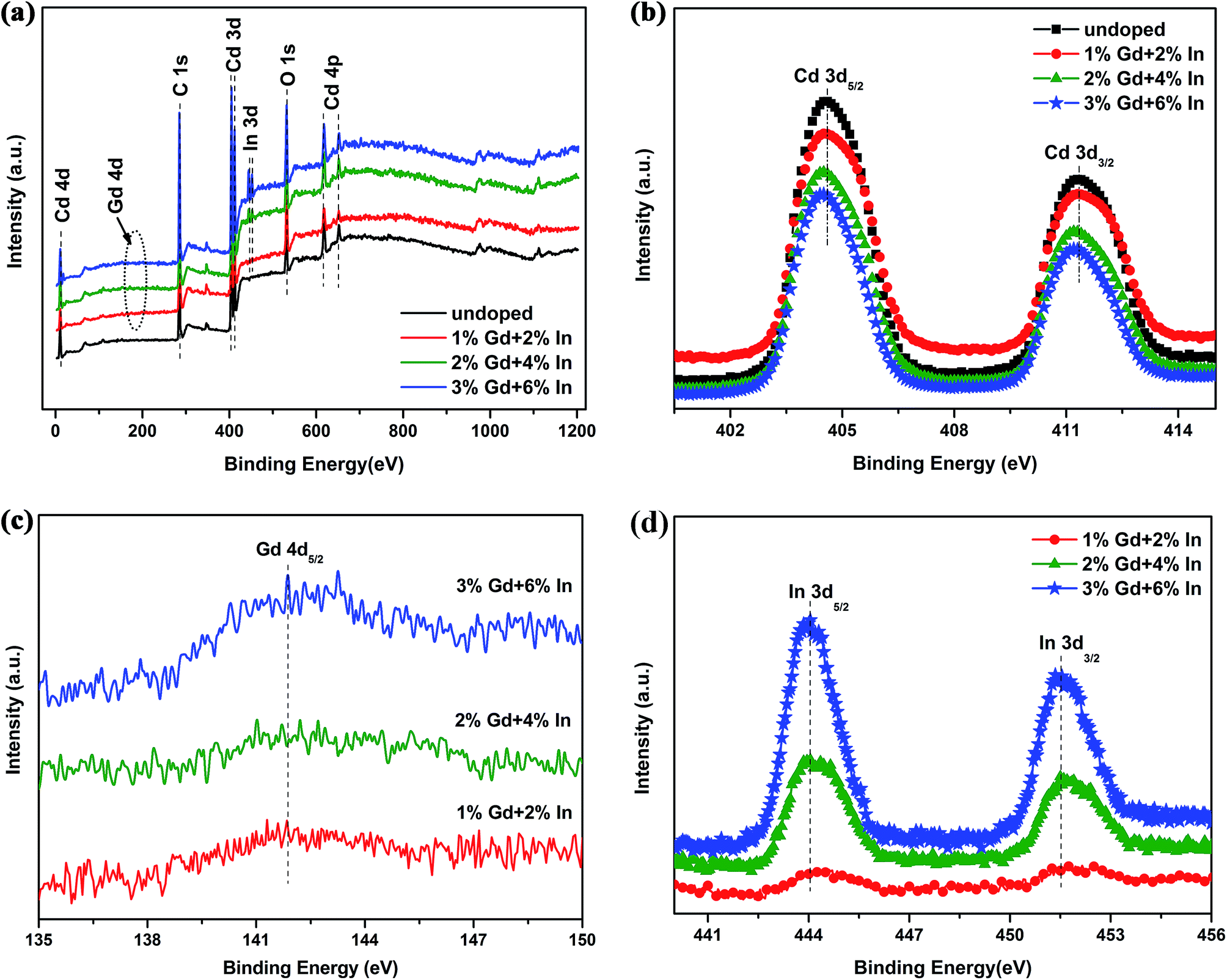 | ||
| Fig. 3 Typical XPS spectra of the CdO films deposited at different Gd and In doping concentrations: (a) survey spectra, and (b–d) narrow scan spectra showing (b) Cd 3d, (c) Gd 4d, (d) In 3d. | ||
 | ||
| Fig. 4 XPS O 1s signals from the CdO films deposited at different Gd and In doping concentrations: (a) undoped, (b) 1 at.% Gd and 2 at.% In, (c) 2 at.% Gd and 4 at.% In, and (d) 3 at.% Gd and 6 at.% In. | ||
The concentrations of gadolinium and indium can be measured from the XPS results. The measured concentrations in the films and the nominal concentrations in the target of gadolinium and indium are shown in Table 1, both are comparable although the measured concentrations are little lower than the nominal concentrations in the targets. The ratios of [O]/[Cd] for these films are also calculated from the XPS results and shown in Table 1. All the ratios are smaller than unity, which confirms the oxygen deficiency in the films. The induced oxygen vacancies serve as shallow donors and are responsible for the n-type conductivity of the films. In addition, with an increase in Gd and In concentrations, the values show an increased trend which implies the decreased deficiency of oxygen in the films, it is due to the substitutions of Cd2+ by either In3+ or Gd3+ ions in the CdO lattice.
| Sample no. | Nominal % of dopant in target material | Dopant % from XPS in thin films | [O]/[Cd] | ||
|---|---|---|---|---|---|
| Gd | In | Gd | In | ||
| CdO | 0 | 0 | 0 | 0 | 0.81 |
| CGIO-1 | 1 | 2 | 0.75 | 1.89 | 0.85 |
| CGIO-2 | 2 | 4 | 1.79 | 3.77 | 0.89 |
| CGIO-3 | 3 | 6 | 2.65 | 5.69 | 0.94 |
The microstructure of semiconductor films has an important effect on the electrical performance for the heterojunction diodes. Typical FESEM images of the CdO and CGIO thin films are displayed in Fig. 5a–d. As shown, all the films are composed of nanograins. The undoped CdO film (Fig. 5a) exhibits a dense morphology with randomized small particles with an average grain size of 40 nm. With the introduction of Gd and In, the films (Fig. 5b–d) become more smooth, continuous, homogeneous and compact, and the average grain size decreases gradually to 37, 26 and 23 nm, respectively, with increasing Gd and In concentrations. The obvious decrease in the grain size may be attributed to the existence of internal strain and lattice distortion or defects induced by the dopant. As the atom size of Gd (2.54 Å) or In (2.00 Å) is larger than that of Cd (1.71 Å), the doping of Gd and In will induce lattice distortion, and the dopant atoms prefer to dwell in/near grain boundary regions in order to reduce lattice distortion. So, more Gd and In atoms locating in/near grain boundaries would prevent grain growth. Therefore, an obvious decrease in grain size is observed for the Gd and In doped CdO films.
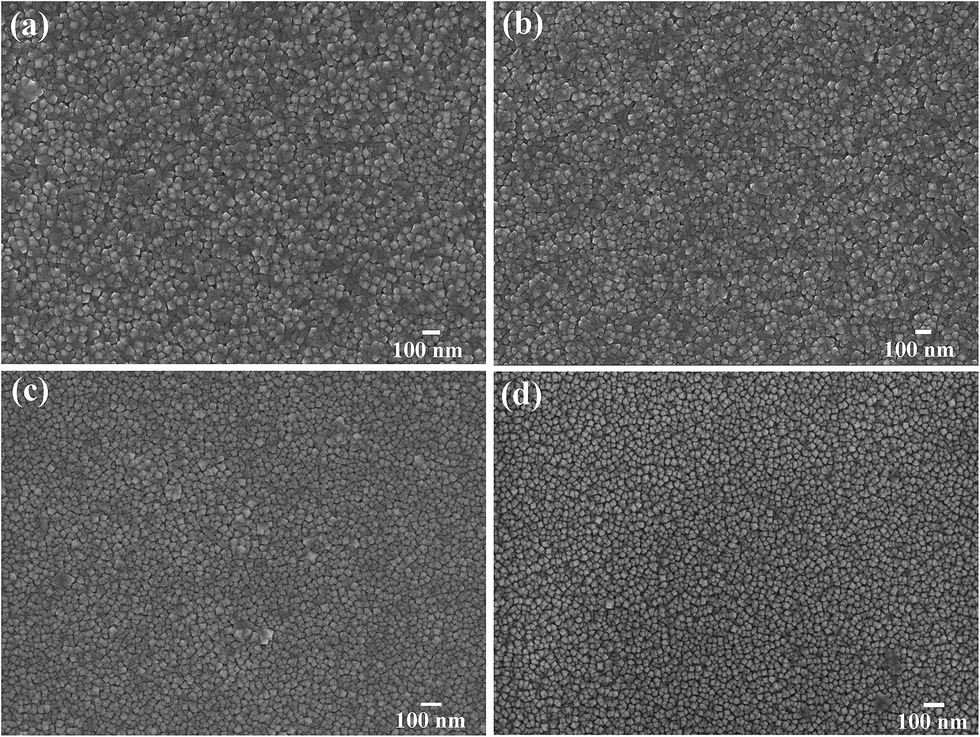 | ||
| Fig. 5 FESEM images of the CdO films deposited at different Gd and In doping concentrations: (a) undoped, (b) 1 at.% Gd and 2 at.% In, (c) 2 at.% Gd and 4 at.% In, and (d) 3 at.% Gd and 6 at.% In. | ||
3.2 Optical and electrical characterization
The optical transparency and band gap of a semiconductor film are very important parameters for their optoelectronic and photovoltaic applications. The optical transmission spectra of CdO and CGIO films are shown in Fig. 6. The optical transmission of the film increases from 83% to 92% in visible spectral region as Gd and In doping level increases. With an increase in Gd and In concentrations, a blue shift in the absorption edge of the film is noteworthy as it leads to an increase in the width of transmission window. The direct optical band gap (Eg) is obtained by a careful analysis of absorption coefficients,23 and it can be determined by extrapolating the linear regions of the plots to zero absorption (see the insert in Fig. 6). It is seen that the doping of Gd and In induces an evident increase of band gap (Eg), for example, from 2.72 eV for undoped CdO film to 3.56 eV for the CGIO film with 2% Gd and 4% In. In general, the conduction characteristics of CdO film are dominated primarily by the electrons generated from oxygen vacancies and Cd interstitial atoms. Compared with the undoped CdO film, doped Gd3+ and In3+ ions on substitution sites of Cd2+ ions or in interstitial sites of the CdO lattice will provide more electrons and holes and hence increase the carrier concentration, which would widen the band gap according to the Burstein–Moss (B–M) effect.24,25 However, with the content of Gd and In increasing to 3% and 6%, respectively, the band gap decreases inversely to 3.26 eV. This sudden shrinkage in heavy donor doping may be attributed to the comprehensive effect of the band gap renormalization, the formation of impurity phase, and localization effect of transition metal. Firstly, the band gap renormalization can be caused by the electron-dopant interactions and electron–electron Coulomb and exchange interactions within the conduction band. Similar shrinkage of band gap is also observed with other trivalent dopants (Y, Sm, Dy, Sc and Al). Moreover, the 4f-electrons of the impurity dopant ions can add a new parameter (like 4f–5d transition) to the energy band spectrum of CdO. Thus, due to the doping of Gd3+ and In3+, the band tailing or impurity band becomes broader and reaches finally and merges the bottom of the conduction band causing the sudden decrease in the band gap. Secondly, according with the XPS analysis, oversaturated indium atoms are precipitated at grain boundary to form impurity phase of In2O3, which act as defect levels to appear between the valence and conduction band of CdO and caused finally the optical band gap decreasing. Thirdly, as the substitute of Cd2+ ions, the 5d-electrons of In3+ ions can engender a spin exchange interaction with the electrons of the semiconductor band edge and then the optical band gap begin to red shift. Due to these reasons, a decrease in band gap is observed for over doping of Gd and In. Despite all of these, the band gap values of all the CGIO films are optimum match for the solar spectrum. | ||
| Fig. 6 Optical transmission spectra of the CdO films deposited at different Gd and In doping concentrations on quartz glass substrate. The inset image shows the relation between (αhν)2 and hν of the sample films. | ||
From Table 2, it is observed that the doping of Gd and In can cause a marked reduction in the resistivity. With an increase in Gd and In concentrations, the resistivity of the films decreases from 2.48 × 10⁻³ Ω cm to 7.6 × 10⁻⁵ Ω cm. The decrease in resistivity can be also associated with the increase in carrier concentration from 1.08 × 1020 cm−3 to 1.47 × 1021 cm−3 and the mobility from 77.5 cm2 V−1 s−1 to 115.9 cm2 V−1 s−1. The enhanced conductivity plays a very important role in the successful fabrication of the Schottky diodes. The low resistivity of the CdO films will lead to a wide depletion width at the junction between the CGIO layer and Al electrode, which can restrain the tunneling current through the barrier and obtain a good rectifying effect.
| Sample no. | Electrical properties | ||
|---|---|---|---|
| ρ (×10−4 Ω cm) | n (×1020 cm−3) | μ (cm2 Vs−1) | |
| CdO | 24.8 | 1.08 | 77.5 |
| CGIO-1 | 6.85 | 3.84 | 84.6 |
| CGIO-2 | 1.92 | 9.7 | 96.5 |
| CGIO-3 | 0.76 | 14.7 | 115.9 |
3.3 Current–voltage characteristics of the Al/n-CdO/p-Si/Ag heterojunction diode
The current density–voltage (J–V) characteristics of the CdO/p-Si and CGIO/p-Si heterojunction diodes under dark condition are shown in Fig. 7. All the curves are asymmetrical and non-linear. These diodes exhibit good rectification behavior. The rectification ratio (RR) is calculated as the ratio of forward current density (JF) to the reverse current density (JR) at a certain applied voltage (V), i.e., RR = (JF/JR)V. The plots of RR versus V for the diodes are shown in the inset of Fig. 7. The RR values are found to be dependent on the dopant concentrations and the applied bias. The grain boundary scattering-limited mobility plays an important role in the decreased in RR values, this poor transport properties could not provide effectively a direct electrical pathway for the electrons. It can also be seen that the currents increase linearly at lower applied voltages (0.1–0.4 V), it suggests an ohmic conduction. With the increase of applied voltage (0.4–2.0 V), the forward currents follow approximately an exponential trend. Typical logarithmic plots of the J–V characteristics at relatively high forward voltage regions are shown in Fig. 8. As shown, the current density can be expressed by a power-law, i.e., J ∝ Vm. The curve (Fig. 8 inset) shows that the m values calculated from the slopes in Fig. 8 decrease from 2.23 to 1.97. The obtained results (m ≈ 2) suggest a space current limited current (SCLC) conduction mechanism corresponding to the case where no traps are present or all traps are filled, and in SCLC region, the current increases quadratically with the bias voltage. The experimental values of Schottky barrier height (Φb) and ideality factor (n) are determined from the current axis intercept and the slope of the linear region of the forward bias semi-logJ–V curve, respectively.26 The calculated values are presented in Table 3. It shows that with the increase in Gd and In doping concentrations, the n values decrease from 2.27 to 1.69, while the Φb values increase from 0.55 to 0.61 eV. The obtained n values confirm the presence of a combination of recombination and diffusion currents in these diodes, and the decrease in ideality factor may be attributed to the improved interface state of Cd1−x−yGdxInyO/p-Si diodes. It is consistent with the XPS analysis (Table 3 and Fig. 4), and it shows that there are fewer oxygen-related defect centers in the CGIO films. This improvement can greatly reduce the defect-assisted tunneling probability. The increase in values of the Φb is mainly due to fewer low Schottky barrier height regions with Gaussian distribution existing at the interface, and more electrons have sufficient energy to overcome the Φb when dopant concentrations increase. Moreover, the deviations in the ideality factor may be due to the spatially inhomogeneous barrier height and the potential fluctuations at the interface that consist of the low and high barrier heights,27,28 i.e. the current through the diode will flow preferentially through the lower barriers in the potential distribution. So, the interface states play an important role on determination of Schottky barrier height and other electronic parameters and these can affect diode performance, stability and reliability. The largest value of Φb (0.61 eV) in present work is found to be smaller than 0.87 eV reported by Siad et al.28 and Sağlam et al.29 for the Al/p-Si Schottky barrier diodes. The case may be ascribed to CdO or CGIO films modifying the effective barrier height by influencing space charge region of the Si substrate. On the other hand, for this metal–oxide semiconductor/p-Si heterostructure diodes, the results obtained by Farag. et al.30 are slightly inferior to ours. He has shown that the values of n and Φb were 2.1 and 0.68 eV for 2 at.% Zn doped CdO/p-Si diodes, respectively.
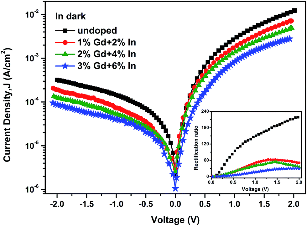 | ||
| Fig. 7 Current density–voltage (J–V) characteristics of the Al/n-Cd1−x−yGdxInyO/p-Si/Ag heterojunction diodes in dark. The inset image shows the rectification ratio dependence of the applied bias. | ||
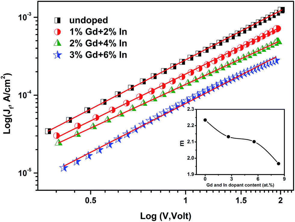 | ||
| Fig. 8 Current density–voltage (J–V) characteristic in a double logarithmic plot for the Al/n-Cd1−x−yGdxInyO/p-Si/Ag heterojunction diodes in SCLC region. The inset image shows dopant content dependence of the slope m. | ||
| Sample no. | Dark | Illumination | |||||||||
|---|---|---|---|---|---|---|---|---|---|---|---|
| n | Φb (eV) | Rs (Ω cm2) | Rsh (Ω cm2) | Rs (Ω cm2) | Rsh (Ω cm2) | Voc (V) | Jsc (mA cm−2) | FF (%) | η (%) | S (mA W−1) | |
| CdO | 2.27 | 0.55 | 161.2 | 6215.8 | 34.5 | 483.9 | 0.49 | 0.8 | 51 | 0.2 | 45.6 |
| CGIO-1 | 2.11 | 0.57 | 272.2 | 9978.6 | 21.1 | 392.2 | 0.58 | 1.1 | 52 | 0.3 | 828.3 |
| CGIO-2 | 1.93 | 0.58 | 410.4 | 15318.6 | 14.2 | 92.3 | 0.80 | 5.6 | 59 | 2.6 | 1357.9 |
| CGIO-3 | 1.69 | 0.61 | 689.3 | 21657.2 | 11.8 | 46.2 | 1.04 | 11.4 | 63 | 7.5 | 1708 |
The series resistance (Rs) and shunt resistance (Rsh) are determined from the plot of junction resistance (Rj), against voltage (V), where Rj = ∂V/∂J, as shown in Fig. 7. The obtained data are presented in Table 3. It clearly shows that with the increase in the dopant concentrations, the Rs value increases from 161.2 to 689.3 Ω cm2, which may be attributed to the increase in the number of free charge carriers, by either bond breaking or de-trapping mechanism,31 the Rs really plays an important current-limiting role for this heterostructure. The Rsh reflects the existence of defects that provide forward leakage path to minority charge carriers and grain boundaries are the source of the defects in case of polycrystalline materials. So, the FESEM image in Fig. 5d shows the increase of defects due to Gd and In doping, it can explain the reason why the Rsh value increases from 6.2 × 10³ to 2.2 × 10⁴ Ω cm2.
3.4 Photovoltaic properties of Al/p-Si/n-CdO/Ag heterojunction diode
The current density–voltage characteristics of the heterojunction diodes under an illumination intensity of 100 mW cm−2 are showed in Fig. 9. It can be seen that the current under illumination is higher than the dark current by about one or two order of magnitude. It is mainly due to the generated electron–hole pairs, i.e. neutral excitons, and these charges contribute to the photocurrent as a result of the light absorption. The light illumination does not change significantly the forward current of the diodes, whereas the current in the reverse direction is increased by illumination. It indicates that the rectification effect is weakened and the diodes exhibit more ideal behavior under illumination. With an increase in the doping concentrations, the number of photo-generated carrier charges is increased at the interface, the Cd1−x−yGdxInyO layer absorbs the photons (Fig. 10) and the photo-generated carriers are sufficiently energetic to cross the barrier height, and this leads to high jump probability of charge carriers between CdO or CGIO film and Si layer. Moreover, the Cd1−x−yGdxInyO film has better transparency for the visible light and allows more light transmit into the Si layer. Thus, the diodes become more sensitive to light, that is, the addition of Gd and In gives a rise of the photocurrent. The Rs and Rsh in the photovoltaic diode are mainly influenced by the movement of photocurrent. They are calculated from Fig. 9 and also compiled in Table 3. As shown, the values of Rs and Rsh decrease significantly by one to three orders of magnitude than those obtained in dark. With the increase in doping levels, the Rs value decreases from 34.5 to 11.8 Ω cm2, and the Rsh value also decreases from 483.9 to 46.2 Ω cm2. For the best diode performance, the highest Rsh value and the lowest Rs value are desired. So, though the Rsh values of our diodes are still higher than those of the Rs values, but the low Rsh values can cause power losses in diodes by providing an alternate current path for the photo-generated current. The filling factor (FF) and conversion efficiency (η) can be calculated by the solar cell parameters.32 These parameter, such as open circuit voltage (Voc), short-circuit current density (Jsc), current density (Jm) and potential maximum power point (Vm) can be observed directly in the inset of Fig. 9. And the calculated results can also be seen in Table 3. The results indicate that the heterojunction solar cells have good photovoltaic abilities. The Voc for the undoped CdO is found to be close to that of conventional Si solar cells. With the increase in dopant concentrations, the Voc value increase from 0.49 to 1.04 V and the Jsc value increase consistently from 0.8 to 11.4 mA cm−2. The highest value of Voc for the studied diodes is higher than those of previous reported heterojunction solar cells.33−36 The detailed comparison is presented in Table 4. The remarkable improvement in Jsc in our case may be strongly related to the enhancement of the diffusion (built-in) potential (Φbi). The Schottky barrier height (Φb) and the diffusion potential (Φbi) can be consistently explained by the following equation: Φb = Ec − Ef + Φbi, we tentatively assume that the potential difference of the Fermi level (Ef) and the top of the conduction band in the Si layer are constant, so Φbi is increased with the increase in Φb. Due to the enhancement of Φbi, more photo-generated electron–hole pairs diffused at the interface of Cd1−x−yGdxInyO/p-Si are dissociated rapidly. Thus, more separated electrons (or holes) are transported towards the cathode (or anode) and then the larger Jsc can be collected. Moreover, the lattice mismatch and different thermal expansion coefficient between Cd1−x−yGdxInyO film and Si layer can induce the interface defects generation. However, it can be seen from the XRD and XPS analysis that the preferential orientation of (200) plane increases constantly and the oxygen vacancies decrease continually with the increase in doping levels. The comprehensive effect of these factors will cause a decrease in the interface defects and the charge recombination centers in space charge region, and then lead to the recombination current decreases gradually. Thus, the successful suppression of charge recombination is favorable for Jsc increasing. Similarly, the modified interface state correlates with the continuing increased Voc, because Voc is affected significantly by the trapping sites and charge recombination centers existing at the interface and grain boundary of the CGIO film. As these defects decrease continuously, the kinetic balance between electron photogeneration and loss achieves gradually optimal effect. That is, the higher crystallinity property and carrier density for the CGIO film, the faster photo-generated electrons transport to the anode contact. Thus, the shortened electron pathway and prolonged electron lifetime can reduce the charge recombination loss, and then increase greatly Voc for the photodiodes. In addition, the reduction of Rs in the diodes can further ensure a higher Voc due to the decrease of the potential drop at the interface of active layer and cathode. Along with the enhancement of Voc and Jsc, the FF value increases from 51% to 63%, for laboratory cells, the FF value is expected to be over 70% and the decrease in modules is indicative of higher series resistance. In general, a recombination current during the photovoltaic operation might suppress the power conversion efficiency. In our research, the power conversion efficiency (η) increases from 0.6% to 7.5%, it suggests that the interface states are improved and/or the interfacial oxide layer is decreased, consequently, electron transport would become faster and thus boost the charge transfer efficiency. The comparison in Table 4 shows that although the power conversion efficiency has been improved greatly by doping of Gd and In, our value is not the highest. The lattice mismatch between CdO (CGIO) film and Si layer may also decrease the power conversion efficiency. | ||
| Fig. 9 Current density–voltage (J–V) characteristics of Al/n-Cd1−x−yGdxInyO/p-Si/Ag heterojunction diodes under 100 kW cm−2 illumination power. | ||
 | ||
| Fig. 10 Schematic energy band diagrams of the Al/n-Cd1−x−yGdxInyO/p-Si/Ag heterojunction diode under the dark and illumination condition, respectively. | ||
To compare the relative photoconductivity sensitivity of the device to the illumination, the current sensitivity or optical response S = [IIll − IDark]/[PIn] (mA W−1) is used, where IIll and IDark are the currents measured at 2 V forward voltages under illumination and in dark, respectively. The results can also be seen in Table 3. The S value increases from 45.6 mA W−1 to 1708 mA W−1 with the increase in Gd and In doping levels, it means that dopants make an important contribution to the electrical and optical properties of the n-CdO/p-Si diodes. So, our study may open the possibilities of systematic research and further development in the Al/p-Si/n-CdO/Ag photovoltaic device.
3.5 The band structure of the heterojunction diode
The band structure of n-CdO/p-Si heterojunction diode can be constructed using Anderson model.37 In the construction of the band structure, the effect of interfacial state and variance of the Fermi energy are neglected. Fig. 11 shows the constructed band structure of the n-CdO (CGIO)/p-Si heterojunction diode under forward bias. In this diagram, the values of band gap of Eg (CdO/CGIO) = 2.82–3.56 eV and Eg (Si) = 1.12 eV, the electron affinity for CdO, χ(CdO) = 4.51 eV and the electron affinity for Si, χ(Si) = 4.05 eV are used. As shown, the conduction-band offset is ΔEc = χ(CdO) − χ(Si) = 0.46 eV, and the valance-band offset is ΔEv = Eg (CdO/CGIO) − Eg(Si) + ΔEc = 2.16–2.9 eV. ΔEv has a higher value than the ΔEc. This means that, the energetic barrier for electrons is much lower than that for holes; therefore, the injection of electrons from n-CdO (CGIO) to p-Si is greater than the holes injection from p-Si to n-CdO (CGIO). Under forward bias, electrons can be more easily injected into the p-Si side because of the smaller potential barrier. Therefore, the forward current increases rapidly under a higher voltage bias. Moreover, the injection of electrons into p-Si widens the depletion layer on n-CdO and retards holes injection, leading to early current saturation.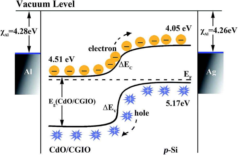 | ||
| Fig. 11 The band structure of the Al/n-Cd1−x−yGdxInyO/p-Si/Ag heterojunction diode under forward bias. | ||
4. Conclusions
Highly transparent and conductive Gd and In doped films were deposited on the quartz glass substrates at 473 K by the pulsed laser deposition method, and the as-deposited CGIO films and p-Si wafer were used as n-type and p-type semiconductors to fabricate the Al/n-Cd1−x−yGdxInyO/p-Si/Ag heterojunction diode. Several conclusions can be derived.1. The XRD and XPS results indicated that Gd3+ and In3+ ions occupied locations in interstitial positions and/or Cd2+ ion vacancies. All the thin films were homogeneous and the size of nanograins decreased from 40 nm to 23 nm with the introduce of Gd and In.
2. The optical band gap of CdO thin film increased firstly from 2.72 to 3.56 eV and then decreased to 3.26 eV by introducing Gd and In dopant. The band gap widening of CGIO thin films can be well explained by the combination of band gap renormalization and Burstein–Moss effect. The high optical transparency (∼85%) and widened band gap can render the nanostructured CGIO thin film a promising candidate for optoelectronic applications.
3. The electrical properties of the Al/n-Cd1−x−yGdxInyO/p-Si/Ag heterojunction diodes have been investigated by current density–voltage (J–V) characteristics. The dark J–V characteristics of the diodes showed a rectification behavior. At lower voltages, the dark forward J–V characteristics can be explained on the basis of thermionic conduction mechanism, while at higher forward voltages, the dark current was space charge limited conduction (SCLC) dominated by a single trap level with exponential traps. The reverse bias current density was interpreted in terms of the Schottky mechanism. With the increase in doping levels, the ideality factor (n) of diodes decreased gradually from 2.27 to 1.69, and exhibited more ideal behavior.
4. Under illumination with intensity of 100 mW cm−2, the Al/3% Gd and 6% In doped CdO/p-Si/Ag heterojunction diode showed the best values of open circuit voltage, Voc = 1.04 V and the short circuit current density, Jsc = 11.4 mA cm−2. Along with the enhancement of Jsc and Voc, the filling factor (FF), power conversion efficiency (η) and current sensitivity (S) of diodes also increased with increasing doping concentrations. This may endue Al/CGIO/p-Si/Ag heterojunction diode the possibility of further development in photovoltaic device or solar cell application.
Acknowledgements
This work was supported by the Foundation of National Key Basic Research and Development Program (no. 2010CB631001), the National Nature Science Foundation (Grant no. 31070841) and the Program for Changjiang Scholars and Innovative Research Team in University.References
- S. J. Clark, J. Robertson, S. Lany and A. Zunger, Phys. Rev. B: Condens. Matter Mater. Phys., 2010, 81, 115311 CrossRef.
- I. Akyuz, S. Kose, E. Ketenci, V. Bilgin and F. Atay, J. Alloys Compd., 2011, 509, 1947 CrossRef CAS PubMed.
- A. K. Singh, A. Janotti, M. Scheffler and C. G. Van de Walle, Phys. Rev. Lett., 2008, 101, 055502 CrossRef.
- X. Chen and S. S. Mao, Chem. Rev., 2007, 107, 2891 CrossRef CAS PubMed.
- J. A. A. Selvan, A. E. Delahoy, S. Guo and Y.-M. Li, Sol. Energy Mater. Sol. Cells, 2006, 90, 3371 CrossRef PubMed.
- H. Kim, C. M. Gilmore, A. Pique, J. S. Horwitz and D. B. Chrisey, J. Appl. Phys., 1999, 11, 6451 CrossRef PubMed.
- M. Yan, M. Lane, C. R. Kannewurf and R. P. H. Chang, Appl. Phys. Lett., 2001, 78, 2342 CrossRef CAS PubMed.
- R. K. Gupta, K. Ghosh, P. Patel and P. K. Kaho, Appl. Surf. Sci., 2009, 255, 6252 CrossRef CAS PubMed.
- O. Vigil, L. Vaillant, F. Cruz, A. Morales-Acevedo and G. Contreras-Puente, Thin Solid Films, 2000, 361, 53 CrossRef.
- P. L. Chen, X. Y. Ma, D. S. Li, Y. Y. Zhang and D. R. Yang, Appl. Phys. Lett., 2007, 90, 251115 CrossRef PubMed.
- D. Ma, Z. Ye, L. Wang, J. Huang and B. Zhao, Mater. Lett., 2003, 58, 128 CrossRef.
- L. R. Gutierrez, J. J. C. Romero, J. M. P. Tapia, E. B. Calva, J. C. M. Flores and M. O. Lopez, Mater. Lett., 2006, 60, 3866 CrossRef PubMed.
- M. Lorenz, E. M. Kaidashev, H. Von Wenckstern, H. Hochmuth, A. Rahm, H. C. Semmelhack and M. Grundmann, Solid-State Electron., 2003, 47, 2205 CrossRef CAS.
- Y. Yang, S. Jin, J. E. Medvedeva, A. J. Freeman and T. J. Marks, J. Am. Chem. Soc., 2005, 127, 8796 CrossRef CAS PubMed.
- B. J. Zheng, J. S. Lian, L. Zhao and Q. Jiang, Vacuum, 2011, 85, 861 CrossRef CAS PubMed.
- F. F. Yang, L. Fang, S. F. Zhang, L. Li and G. Z. Fu, J. Cryst. Growth, 2006, 297, 411 CrossRef CAS PubMed.
- J. C. Lin, K. C. Peng, C. A. Tseng and S. L. Lee, Surf. Coat. Technol., 2008, 202, 5480 CrossRef CAS PubMed.
- R. K. Gupta, K. Ghosha, R. Patel and P. K. Kahol, J. Alloys Compd., 2011, 509, 4146 CrossRef CAS PubMed.
- C. Barret and T. B. Massalski, Structure of Metals, Petgamon, Oxford, 1980, p. 1923 Search PubMed.
- Y. S. Vidya, K. S. Anantharaju, H. Nagabhushana and S. C. Sharma, Spectrochim. Acta, Part A, 2015, 135, 241 CrossRef CAS PubMed.
- K. H. Lee, H. W. Jang, K. B. Kim, Y. H. Tak and J. L. Lee, J. Appl. Phys., 2004, 95, 586 CrossRef CAS PubMed.
- A. W. C. Lin, N. R. Armstrong and T. Kuwana, Anal. Chem., 1977, 49, 1228 CrossRef CAS.
- F. Javier Yusta, M. L. Hitchman and S. H. Shamlian, J. Mater. Chem., 1997, 7, 1421 RSC.
- E. Burstein, Phys. Rev., 1954, 93, 632 CrossRef CAS.
- T. S. Moss, Optical Properties of Semiconductors, Butterworths, London, 1961 Search PubMed.
- F. Yakuphanoglu, Appl. Surf. Sci., 2010, 257, 1413 CrossRef CAS PubMed.
- S. H. Werner and H. H. Guttler, J. Appl. Phys., 1991, 69, 1522 CrossRef PubMed.
- M. Siad, A. Keffous, S. Mamma, Y. Belkacem and H. Menari, Appl. Surf. Sci., 2004, 236, 366 CrossRef CAS PubMed.
- M. Sağlam, A. AteŞ, M. A. Yıldırım, B. Güzeldir and A. Astam, Curr. Appl. Phys., 2010, 10, 513 CrossRef PubMed.
- A. A. M. Farag, M. Cavas and F. Yakuphanoglu, Mater. Chem. Phys., 2012, 132, 550 CrossRef CAS PubMed.
- K. S. Karimov, M. M. Ahmed, S. A. Moiz and M. I. Federov, Sol. Energy Mater. Sol. Cells, 2005, 87, 61 CrossRef CAS PubMed.
- J. Santos-Cruz, G. Torres-Delgado, R. Castanedo-Pérez, S. Jimenez-Sandoval, J. Márquez-Marín and O. Zelaya-Angel, Sol. Energy Mater. Sol. Cells, 2006, 90, 2279 CrossRef PubMed.
- S. J. C. Irvine, D. A. Lamb, V. Barrioz, S. Ruge, Hankey and G. Kartopu, Thin Solid Films, 2011, 520, 1167 CrossRef CAS PubMed.
- J. Liu, A. W. Hains, J. D. Servaites, M. A. Ratner and T. J. Marks, Chem. Mater., 2009, 21, 5258 CrossRef CAS.
- Y. Li, R. Mastria, A. Fiore, C. Nobile and G. Gigli, Adv. Mater., 2009, 21, 4461 CrossRef CAS.
- B. M. Basol, V. K. Kapur and M. L. Ferris, J. Appl. Phys., 1989, 66, 1816 CrossRef CAS PubMed.
- A. G. Milnes and D. L. Feucht, Heterojunctions and Metal-Semiconductor Junctions, Academic, New York, 1972 Search PubMed.
| This journal is © The Royal Society of Chemistry 2014 |