
Self-assembled zirconia nanotube arrays: fabrication mechanism, energy consideration and optical activity†
Ahmad W. Amera,
Seifallah M. Mohameda,
Ahmed M. Hafeza,
Siham Y. AlQaradawib,
Amina S. Aljaberb and
Nageh K. Allam*a
aEnergy Materials Laboratory (EML), Physics Department, School of Sciences and Engineering, The American University in Cairo, New Cairo 11835, Egypt. E-mail: nageh.allam@aucegypt.edu
bDepartment of Chemistry and Earth Sciences, Qatar University, P. O. Box 110003, Doha, Qatar
First published on 12th August 2014
Abstract
We present a comprehensive roadmap for the precise control of the dimensions and optical properties of anodically fabricated zirconia nanotubes. The effects of anodization time, applied voltage, solvent composition, as well as fluoride and water content are investigated. The length of the resulting nanotubes showed a strong dependence on the concentration and mobility of F− ions, whilst O2− ion content was found to play a key role in controlling the nanotube wall thickness. A new insight into the formation of Zirconia nanotubes is introduced and discussed based on the Point Defect Model (PDM). Also, the energy consumption in the fabrication process of the nanostructured electrodes is modelled based on the involved thermodynamics and kinetic aspects. The effect of the dimensions of the nanotubes on the optical characteristics of the arrays was studied using Finite Difference Time Domain (FDTD). The results show a decrease in transmittance with increasing length and wall thickness, and decreasing pore size of the nanotubes. The reported results provide deep insight into the structure–property relationships of ZrO2 nanotubes, which will be of great help in large-scale industrial applications.
1 Introduction
With emerging nanoscale technologies, the need for developing efficient protocols for the synthesis of nanostructured materials that can be easily transferred to industry has become dire. Indeed, such protocols have been established in many fields in order to satisfy application-specific requirements, including synthesis of nanoparticles,1,2 nanowires,3,4 nanotubes,5–7 and other nanostructures.8–10 For instance, efficient solar-driven water splitting through the use of nanotube photoanodes has been a challenge since the success of the Honda–Fujishima experiment.11 Many factors, such as the aspect ratio, surface area, surface roughness, and wall thickness,12,13 form specific criteria that must be met in order to achieve efficient hydrogen production.In this sense, the field of metal oxide nanotube synthesis has gained special attention throughout the past 10 years, owing to the wide spectrum of applications that depend on their unique properties. Zirconium dioxide (ZrO2) nanostructures have emerged as a very promising member of the metal oxide nanotube family. The high stability and biocompatibility of ZrO2 nanotubes allow their use as bio-active systems.14–16 In addition, their wide band gap semiconducting properties can be utilized in multi-functional catalysis.17–19
One highly efficient and facile method for synthesizing ZrO2 nanotubes is anodic oxidation via selective etching of zirconium foil in an electrochemical cell.20,21 Such synthesis route has recently attracted wide attention following its success in the synthesis of the broadly used anodic aluminum oxide membranes (AAO),22,23 where the ease of accurately manipulating nanotube structure and morphology through controlling the process parameters is possible. Furthermore, it is widely accepted that the anodization of Zr foils resembles to a great extent that of titanium foils.20,24–26 To this end, many recent reports attempted to clearly identify the effect of process variables that enable the fabrication of well-defined ZrO2 nanotubes. Lee et al.21 studied the effect of applied voltage (10–30 V) and anodization time (1–60 min) in a typical HF-based electrolyte on the properties of the resulted material. Vertically-aligned nanotubes were attained at 20 V and 20 min. Schmuki et al.25 reported the formation of highly-ordered ZrO2 nanotube arrays at 20 V and an anodization time of 1 hour using NH4F as the etchant. However, using a very similar electrolyte/etchant composition, Zhao et al.26 reported optimum results at 10 V and 3 h of anodization time. Xuan-Yong et al.27 studied the effect of fluoride-to-oxygen (F/O) ratio on the competing processes of chemical etching and anodic oxidation. As the F/O ratio was increased, the nanotubes became more structured and crystalline, and the array length increased until a certain threshold ratio (0.7), above which the nanotubes collapsed. However, the substantially high applied voltage in this study (80 V) renders the process inefficient for large-scale use. Ismail et al.,20 on the other hand, used a relatively low voltage of 20 V to study the effect of fluoride content. Although the crystallinity improved as the amount of NH4F added was increased, confirming Xuan-Yong's observations, the length of the synthesized arrays decreased with increasing fluoride content. Furthermore, the threshold content at which the nanotubes collapsed changed with the decreased voltage. Muratore et al.24 reported a higher optimum F/O ratio of 0.9 when changing the water content instead of the fluoride ion content. Adding more water increased the diameters of the resulted nanotubes by an order of ∼20 nm. Although other studies attempt to shed the light on the combined effect of varying anodization variables,28,29 more combinatorial studies are needed in order to reach a consensus with the optimum combination of process variables, thus taking the first steps towards formulating a market-reliable synthesis protocol for ZrO2 nanotubes.
Herein, we report the effects of a combination of anodization process variables (time, applied voltage, electrolyte composition, fluoride and oxygen ion contents) on the structure and morphology of ZrO2 nanotube arrays. Also, mathematical models have been developed to account for the energy consumption during the fabrication process. Further, the effect of the dimensions of the synthesized nanotubes on their optical properties is investigated both experimentally and theoretically.
2 Experimental
Pure zirconium foils (Alfa Aesar, 99.8% purity) were ultrasonically cleaned in acetone/ethanol and distilled water, respectively. Anodization was done in a two-electrode cell with the zirconium foil as the working electrode and platinum as the counter electrode, in glycerol-based electrolytes containing variable amounts of formamide, H2O, and NH4F. The anodized area was fixed at 10 × 10 mm. The distance between the electrodes was fixed at 20 mm, and the operation temperature was fixed at room temperature (approximately 23 °C). Time-dependant anodization current was tracked on 5 min intervals. Anodization was performed using an Agilent E3612A DC power supply. The morphology of the as-anodized samples was studied using a LEO Supra 55 Field Emission Scanning Electron Microscope (FESEM). Specimens were annealed in a LINDBURG Programmable Furnace model N41/M 29667. The crystal structure of as-anodized and annealed samples was studied using a PANalytical X'Pert PRO XRD diffractometer. The optical properties of the anodized foils were measured using a home-made setup that was installed into a Newport QE-PV-SI QE/IPCE instrument. Finite Difference Time Domain simulations were implemented on a computer-written code. The source used was a Gaussian pulse source having a central frequency (fc) of 1498.96229 THz, and a pulse width (w) of 2997.92 THz. For detection, two observation planes were positioned at the top and the bottom of the nanotubes to measure the transmittance and the absorbance, respectively. A lorentzian model was used for simulating the permittivity–frequency plot, along with eye curve-fitting in order to match the simulation model with the experimental results done on ZrO2 nanotubes.3 Results and discussion
3.1 Effect of anodization conditions
To study the effect of solvent composition on the competing processes of chemical etching and oxidation, Zr foils were anodized in glycerol-based electrolytes containing different formamide (FA) contents, while keeping the NH4F and H2O concentrations at 1 wt% and 4 wt%, respectively. Fig. S1† shows the resulted ZrO2 nanotube arrays. Uniform nanotube arrays were obtained in electrolytes containing FA up to 40%. Note the changing morphology of the nanotubes from hexagonal in pure glycerol electrolyte (Fig. S1(a)†), to circular nanotubes as FA content was increased to 10% and 20% (Fig. S1(b and c)†), and back again to hexagonal shape at 30% and 40% FA (Fig. S1(d and e)†). Note also that the most ordered nanotube arrays were obtained in electrolytes with 20% FA, Fig. 1(a). Notably, the top of the nanotubes grown in electrolytes with 10 and 30% FA were covered with debris, which basically consists of detached nanotubes that may have fallen off the substrate during post-anodization ultrasonic cleaning. The nanotubes grown in electrolytes containing 40% FA were covered with a 2μm-thick layer of amorphous material, which indicates corrosion of the top ends of the nanotubes as a result of the high F− ion mobility.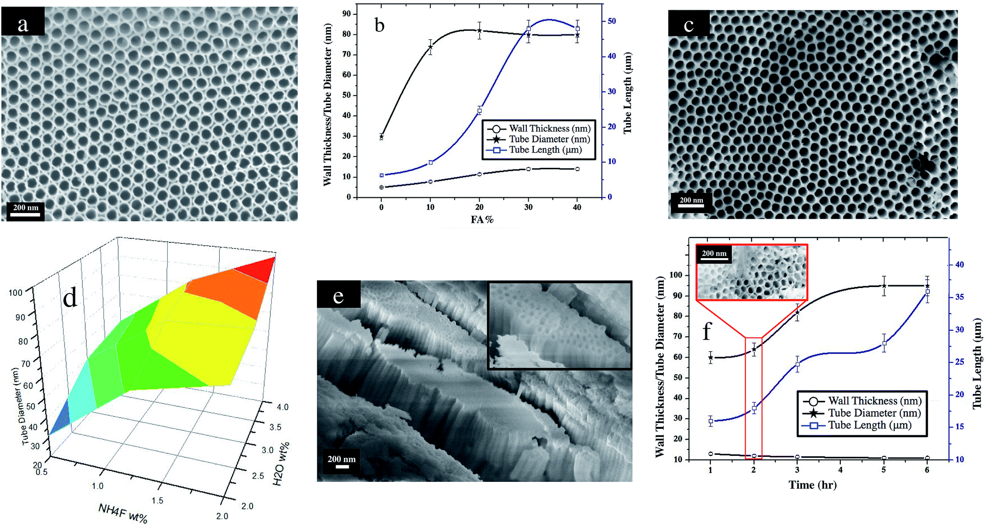 | ||
| Fig. 1 (a) FESEM images of as-grown ZrO2 nanotube arrays via anodic oxidation for 3 h @50 V in glycerol electrolytes containing 20vol% FA, 4 wt% H2O and 1 wt% NH4F (b) variation of the ZrO2 nanotube dimensions with FA content. (c) Same as panel (a) but with 2 wt% H2O and 2 wt% NH4F. (d) 3-D plot illustrating the effect of varying H2O and NH4F content in the electrolytes on the as-anodized ZrO2 nanotube diameters. (e) Same as panel (a) but under applied voltage of 30 V. (f) Variation of ZrO2 nanotube dimensions with anodization time. Inset shows a representative FESEM image of the sample anodized for 2 h. | ||
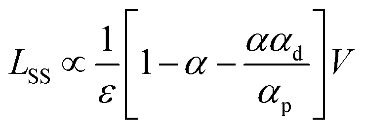
Fig. 1(b) shows the variations of the lengths, diameters, and wall thicknesses of the nanotube arrays fabricated in electrolytes containing different FA contents. Note the increase in the nanotube length with increasing the FA content in the electrolyte from 10% to 30% followed by a plateau until 40% FA. At 50% FA, the Zr foil was cut into two pieces at the electrolyte/air interface. The nanotube wall thickness showed a similar behavior to the change in length. Nanotube diameter, on the other hand, showed a much earlier plateau (near 10%). Fig. S1(f)† shows the time-dependant anodization current curves for samples anodized in electrolytes containing different FA contents. Once the Zr foil is immersed in the electrolyte, the current increases until an insulating passive layer builds up (typically an oxide), resulting in a gradual decrease in current until reaching a steady state. The steady state current (ISS) shows an ohmic dependence on the applied voltage (V) and the combined resistance of a bi-layer passive film as predicted by the second generation of the Point Defect Model,30 i.e.
 | (1) |
Fig. 1(d) is a 3-D plot showing the variation of nanotube diameter with respect to H2O and NH4F contents. Increasing both F− and O2− ion concentrations in the electrolyte resulted in an increase in nanotube diameter. As the F− ion content increased, nanotube length decreased, similar to the anodization of titanium foils.12 Increasing O− ion content, on the other hand, resulted in an increase in the nanotube length.
Anodization time was also varied for samples anodized in glycerol-based electrolytes containing 20% FA, with constant 4 wt% H2O and 1 wt% NH4F contents. Fig. 1(e) shows a representative FESEM image of the fabricated nanotubes after 3 hours of anodization. The full set of FESEM images for the nanotubes fabricated at various time intervals is shown in Fig. S3.† Note that circular nanotubes were obtained for all anodization durations. Note also the presence of detached nanotubes/debris on the surfaces of the foils anodized for 2 hours. The nanotube growth rates shifted from 16 μm h−1 for anodization time of 1 h to 8.5 μm h−1 for anodization time of 2 h. This dramatic shift in the growth rate can be related to the nanotube detachment during the anodization process, where new nanotube arrays replace the detached ones, resulting in shorter nanotubes than expected. The nanotube growth rate of 8.3 μm h−1 remained almost constant for the remaining anodization times (up to 16 h). Fig. 1(f) shows the effect of increasing anodization time on the dimensions of the resulted ZrO2 nanotubes. The effect of anodization time on the nanotube length is fairly linear, as expected at the relatively slow etching rate in the 20% FA electrolyte. In addition, increasing anodization time has an effect on the nanotube diameter similar to that of increasing FA content in the electrolyte, such that more ions would reach the anode at the longer time span (or at higher FA content in the electrolyte). A steady state is reached near 4 h, which can be related to an equilibrium state between chemical etching and anodic oxidation at the top of the array. In contrast to increasing FA content, however, the wall thickness is decreasing as the anodization time increases, indicating a lower oxide layer growth rate as compared to the rate of chemical etching. This can be explained in terms of the added O2− ions as FA content increases in the electrolyte.27 This increase may be the reason behind the increasing wall thickness (i.e. the increasing oxide layer on the walls) as the FA content increases. The absence of excess O2− at a constant FA content, would favor the rate of chemical etching as anodization period increases. Thus, wall thickness would be expected to decrease as well.
ZrO2 nanotube arrays were also synthesized using different applied anodization voltages (10–50 V) while keeping all other anodization parameters intact. Fig. S4† shows the grown nanotubes at 10 and 30 V. While no nanotube structures were observed at 10 V, increasing the voltage resulted in the formation of nanotube arrays with larger tube diameters of 25 and 82 ± 1 nm for 30 and 50 V, respectively. The nanotubes synthesized at 30 and 50 V had a nearly-identical wall thickness of 10.5 ± 1 nm. The tube length, however, showed an increase until an applied potential of 30 V reaching a length of 40 ± 0.2 μm, in agreement with Wang and Luo.16 This increase in length was followed by a shallow decrease to 24 ± 0.2 μm as the applied voltage increased to 50 V.
3.2 Proposed anodization model
Herein, we present a model for the synthesis of ZrO2 nanotubes via anodic oxidation that fits the obtained results in this and other studies. According to the second and third generations of the Point Defect Model (PDM II-III),30–32 high oxidation state metals, such as Zr, form a bi-layer passive film composed of a barrier layer, and an outer layer where film/electrolyte interactions occur. The growth of both layers depends on the constant generation and annihilation of cation interstitials and anion vacancies. Macdonald et al.33 studied the impedance characteristics of Zr metal immersed in aqueous de-aerated solutions, and concluded the formation of an oxide outer layer, on top of a defective oxide barrier layer. In a later study, Macdonald and Engelhardt32 studied the bi-layer passive film forming on Zr in hydride-rich solutions, and concluded the formation of a hydride instead of an oxide barrier layer, owing to the faster diffusion kinetics of hydrogen as compared to oxygen. In this sense, F− ions are almost twice as fast as O2− ions.34,35 Therefore, it is reasonable to assume the formation of a fluoride barrier layer when Zr metal is immersed in fluoride-rich electrolytes.As immersing the Zr foil into the electrolyte, a defective fluoride layer starts to build up into the metal surface as a result of the constant generation of fluoride vacancies at the foil/electrolyte interface, i.e.,
 | (2) |
 | (3) |
On the other hand, field-assisted dissolution of the barrier layer occurs causing the decrease in the barrier layer thickness (i.e. de-passivation),27,30 i.e.,
| ZrF2 + 4F− + 2H+ → H2ZrF6 | (4) |
In reaction (4), the formation of fluorozirconic acid (H2ZrF6) is the most probable route for Zr metal in fluoride-containing aqueous solutions.36,37 The net thickness of the steady state fluoride barrier layer depends on the fluoride concentration, voltage, pH, and the standard rate constants of the passivation/de-passivation reactions.31 Indeed, the formation of a fluoride-rich layer at the oxide/metal interface has been reported for Zr,38 as well as Tantalum.39,40 Meanwhile, cation interstitials, ejected from the foil's surface, diffuse through the barrier layer towards the barrier layer/electrolyte interface. They then get hydrated/oxidized via the anions in the electrolyte, forming oxides (outer layer),30 i.e.,
 | (5) |
 | (6) |
| ZrO2+ + H2O → 2H+ + ZrO2 | (7) |
In addition, field-assisted dissolution (reaction (8)) and chemical etching (reaction (9)) create pits on top of the metastable outer layer, i.e.,
| ZrO2 + 2H+ → ZrO2+ + H2O | (8) |
| ZrO2 + 6F− + 4H+ → [ZrF6]2− + 2H2O | (9) |
Fig. 2(a) schematically depicts our proposed model. The thickness of the outer layer can surpass that of the barrier layer by 4 orders of magnitude, which is typical for anodization of valve metals.30 Field-assisted dissolution of the outer layer results in surface irregularities, where fluoride ions then locally decrease the thickness of the layer through pitting action on the rough surface21 causing an increase in the electric current across it. This triggers more oxide precipitation at the areas where outer layer thickness is decreased.20 The latter also occurs on the inner walls of the pores,41 resulting in the formation of well-defined nanotube structures.
 | ||
| Fig. 2 (a) A schematic illustrating the anodization of Zr foils in fluoride-rich electrolytes. (b) EDX spectra of the bottoms of detached nanotubes showing a F− ion at% almost double that of Zr. | ||
Thus, the abundance of F− and O2− ions is crucial for the formation of ZrO2 nanotubes with high structural integrity. When 0.5 wt% NH4F was used in the anodization electrolyte, F− ion content was too low to form well-defined nanotubes, especially at low water contents, and a poorly-structured layer of amorphous debris covered the nanotube arrays (Fig. S1†). On the other hand, when the F− ion content was too high, increased F− ion diffusion towards the metal/barrier layer interface leads to the detachment of the outer nanotubular layer, as previously observed with Tantalum,35,40 leading to a decreased nanotube length as mentioned above. Indeed, EDX analysis of the bottoms of the detached nanotube arrays (Fig. 2(b)) showed a non-stoichiometric layer of ZrF2. Increasing FA content caused the acceleration of both F− and O2− ions, thus shifting the reactions equilibria forward, and increasing the rate of nanotube formation.
With respect to increasing the voltage, PDM-II31 predicts the dependence of the steady state barrier layer thickness (LSS) on the applied voltage, i.e.,
 | (10) |
3.3 Crystallization of the nanotubes
The nanotube arrays synthesized in electrolytes containing different FA contents were annealed at 500 °C in air. X-ray diffraction patterns of as-anodized and annealed nanotube arrays are shown in Fig. 3. The as-anodized nanotubes are amorphous, with some peaks appearing at 35°, 37°, 48°, and 64° characteristic of the (002), (101), (102), and (003) facets of hexagonal Zr metal.22 These peaks possibly originated form the substrate. In addition, a trace broad peak lies in the region between 28° and 32°. After annealing, this broad peak is de-convoluted showing three distinct peaks at 28°, 30°, and 31°, which correspond to the (111) facet in the monoclinic oxide phase (28° and 31°) and the (111) facet in the tetragonal oxide phase (30°) (27, 28). Smaller peaks appear near 50°, which correspond to the (220) and (022) facets in the monoclinic oxide phase,22 as well as the (112) facet in the tetragonal oxide phase.27 Note the absence of the characteristic tetragonal phase at 30° in the annealed samples originally grown in electrolytes containing 40% FA. Thus, XRD patterns confirm the formation of ZrO2 nanotubes with dominating monoclinic phase. | ||
| Fig. 3 XRD spectra of (I) as-anodized nanotube arrays, and (II–IV) as-annealed nanotube arrays (500 °C – 4 h) synthesized in glycerol electrolytes containing 0%, 20%, and 40% FA, respectively. M = monoclinic phase; T = tetragonal phase. | ||
3.4 Energy considerations
To formulate a market-reliable synthesis protocol for ZrO2 nanotubes, the total energy used for their synthesis should be calculated. Herein, we calculated the energy required for the individual processes occurring inside the electrolyte during the synthesis process. To this end, the anodization process can be divided into two major processes: (1) the chemical synthesis and dissolution of the oxide layer, and (2) the physical diffusion of ions near the electrolyte/anode interface. The chemical process represented by the formation of the bi-layer passive film at the anode, as well as the evolution of H2 at the cathode can be combined in an overall reaction as follows:| 2Zr (s) + 2H2O (l) + 2NH4F (aq) ⇒ ZrF2 (s) + ZrO2 (s) + 2H2 (g) + 2NH4+ (aq) | (11) |
Following Li's model,42 the minimum work (W) associated with the chemical synthesis can be described as:
| W = (HR − TSR) − (HP − TSP) | (12) |
The electrical energy required for the physical diffusion of ions near the electrolyte/anode interface under applied potential V for time t can be given by:42
| E = V × A × I × t | (13) |
 | (14) |
![[thin space (1/6-em)]](https://www.rsc.org/images/entities/char_2009.gif) 799.436 kJ mol−1.
799.436 kJ mol−1.
Thus, the total energy required for the synthesis of ZrO2 nanotubes via anodization of Zr foils is estimated as 111693.6 kJ mol−1, with the physical diffusion of ions inside the electrolyte being the most energy-consuming step in the anodization process.
3.5 Optical properties
To investigate the optical characteristics of anodized ZrO2 nanotubes, Finite Difference Time Domain (FDTD) calculations were performed, along with experimental characterization for transmittance and absorption of the nanotubes. FDTD is a well-known computational technique that allows the investigation of the optical properties of the nanotubes through observing the propagation of electromagnetic waves throughout the lattice. Along the simulation process, the values for the fields throughout each computational grid are updated, rendering FDTD a very useful tool for the optimization of material optical properties.Fig. 4(a and b) illustrates the model used in the FDTD analysis. Following the work of Ong et al.,45 normal incidence of the electromagnetic waves in the negative Z direction was assumed. The model was built for highly-oriented ZrO2 nanotubes having circular cross-section with an average length of 18 μm, an outer diameter of 64 nm, and a wall thickness of 12 nm. The cell used was surrounded by a matching layer to absorb any reflected electromagnetic waves outside the tubes at all frequencies and angles of incidence.
 | ||
| Fig. 4 (a) A schematic showing the model built for the FDTD calculations, (b) a plot showing the incident, reflected, and transmitted electromagnetic fields in the time domain. (c) Dependence of the relative permittivity of ZrO2 on the frequency of the incident field. (d and e) A comparison between the measured and simulated transmittance and absorption, respectively, for ZrO2 nanotubes having a length of 18 μm, a diameter of 64 nm, and a wall thickness of 12 nm. (f and g) Simulated data for transmittance and absorption of nanotubes having different lengths. (h) Simulated data for transmittance of nanotubes having different wall thicknesses. | ||
ZrO2, being a dispersive material, necessities the accurate calculation of the material's permittivity in order to be able to investigate the optical properties of the nanotubes. For this purpose, density functional theory (DFT) calculations were first performed, using the exchange–correlation functional of Perdew–Burke–Ernzerhof (PBE), to obtain the dielectric function for pure zirconia. Fig. 4(c) shows the real (ε′) and imaginary (ε′′) parts of the dielectric function together with the operating frequency i.e.,
| ε′ = n2 − k2 | (15) |
| ε′′ = 2nk | (16) |
Fig. 4 panels (d and e) show the strong agreement of the measured transmittance and absorbance with the simulated results. Note that the absorbance (A) was measured according to the following relation:
 | (17) |
Because the wall thickness of the nanotubes is very crucial when designing photoactive systems, the effect of increasing wall thickness on the optical properties of the ZrO2 nanotubes was studied using the proposed FDTD model. Fig. 4(h) shows the change in transmittance of the nanotubes as the wall thickness of the nanotubes get thicker, while keeping the outer diameter and the tube length fixed. As shown, the transmittance decreases with increasing the wall thickness of the nanotubes, due to the decrease in the volume of the air column inside the nanotubes, thus increasing the effective index of refraction.45
4 Conclusion
In this article, a roadmap for the effect of synthesis parameters on the morphology and optical properties of ZrO2 nanotubes was presented. Increasing formamide and water contents in the electrolyte, as well as anodization time and voltage till 30 V resulted in an increase in the nanotube lengths and diameters, which was attributed to the increased reaction kinetics. Although increasing F− ion concentration led to increased nanotube diameters, it resulted in a decrease in the length. Similar results were obtained with increasing the anodization potential above 30 V. Nanotubes synthesized in O2−-rich electrolytes exhibited thicker tube walls as compared to those synthesized in electrolytes with lower formamide concentrations. The optimum process conditions were defined as follows: for highly-ordered ZrO2 nanotubes with circular morphology, Zr foils were anodized for 3 h at 50 V in a glycerol-based electrolyte containing 20% FA, 1 wt% NH4F, and 4 wt% H2O. To obtain nanotubes with hexagonal morphology, etchant and water contents were 2 wt%. A model for the anodization of Zr foils was proposed based on the Point Defect Model such that a fluoride barrier layer grows into the metal, on top of which an oxide outer layer precipitates. The effect of nanotube dimensions on their optical properties was studied using FDTD. A good agreement between theoretical and the experimental results allowed for the accurate prediction of the optical properties. Unlike absorption, transmittance of the nanotubes was shown to decrease with nanotube length and wall thickness. The results presented herein provide the general framework for the synthesis of optically-active ZrO2 nanotubes.Acknowledgements
This work was made possible by NPRP Grant no. NPRP 6-569-1-112 from the Qatar National Research Fund (a member of Qatar Foundation).Notes and references
- H. K. Kammler, L. Mädler and S. E. Pratsinis, Chem. Eng. Technol., 2001, 24, 583–596 CrossRef CAS.
- C. Suryanarayana, Mater. Today, 2005, 8, 62 CrossRef.
- N. K. Hassan, M. R. Hashim, M. A. Mahdi and N. K. Allam, ECS J. Solid State Sci. Technol., 2012, 1, P86–P89 CAS.
- V. Lefevre, Nanowires: properties, synthesis and applications, Nova Science Publishers, New York, 2012 Search PubMed.
- H. Dai, Acc. Chem. Res., 2002, 35, 1035–1044 CrossRef CAS PubMed.
- S. Hou, C. C. Harrell, L. Trofin, P. Kohli and C. R. Martin, J. Am. Chem. Soc., 2004, 126, 5674–5675 CrossRef CAS PubMed.
- N. K. Allam, N. M. Diab and N. A. Ghany, Phys. Chem. Chem. Phys., 2013, 15, 12274–12282 RSC.
- N. K. Allam and C. A. Grimes, Mater. Lett., 2011, 65, 1949–1955 CrossRef CAS PubMed.
- N. K. Hassan, M. R. Hashim and N. K. Allam, Phys. E, 2012, 44, 1853–1856 CrossRef CAS PubMed.
- N. K. Hassan, M. R. Hashim and N. K. Allam, Chem. Phys. Lett., 2012, 549, 62 CrossRef CAS PubMed.
- A. Fujishima and K. Honda, Nature, 1972, 238, 37–38 CrossRef CAS.
- K. Shankar, J. I. Basham, N. K. Allam, O. K. Varghese, G. K. Mor, X. Feng, M. Paulose, J. A. Seabold, K. Choi and C. A. Grimes, J. Phys. Chem. C, 2009, 113, 6327–6359 CAS.
- M. Walter, E. Warren, J. McKone, S. Boettcher, Q. Mi, E. Santori and N. S. Lewis, Chem. Rev., 2010, 110, 6446–6473 CrossRef CAS PubMed.
- M. Das, C. Dhand, G. Sumana, A. K. Srivastava, N. Vijayan, R. Nagarajan and B. D. Malhotra, Appl. Phys. Lett., 2011, 99, 143702–143703 CrossRef PubMed.
- C. J. Frandsen, K. S. Brammer, K. Noh, L. S. Connelly, S. Oh, L. Chen and S. Jin, Mater. Sci. Eng., C, 2011, 31, 1716–1722 CrossRef CAS PubMed.
- L. Wang and J. Luo, Mater. Sci. Eng., C, 2011, 31, 748–754 CrossRef CAS PubMed.
- R. Liang, M. Deng, S. Cui, H. Chen and J. Qiu, Mater. Res. Bull., 2010, 45, 1855–1860 CrossRef CAS PubMed.
- D. Fang, Z. Luo, S. Liu, T. Zeng, L. Liu, J. Xu, Z. Bai and W. Xu, Opt. Mater., 2013, 35, 1461–1466 Search PubMed.
- X. Wang, J. L. Zhao, X. Hou, Q. He and C. Tang, J. Nanomater., 2012, 2012, 409571 Search PubMed.
- S. Ismail, Z. A. Ahmad, A. Berenov and Z. Lockman, Corros. Sci., 2011, 53, 1156–1164 CrossRef CAS PubMed.
- W. Lee and W. Smyrl, Curr. Appl. Phys., 2008, 8, 818–821 CrossRef PubMed.
- W. Lee and S. Park, Chem. Rev., 2014, 114, 7487–7556, DOI:10.1021/cr500002z.
- X. H. Huang, G. H. Li, X. C. Dou and L. Li, J. Appl. Phys., 2009, 105, 084306 CrossRef PubMed.
- F. Muratore, A. Baron-Wiechec, T. Hashimoto, P. Skeldon and G. E. Thompson, Electrochem. Commun., 2010, 12, 1727–1730 CrossRef CAS PubMed.
- H. Tsuchiya, J. M. Macak, L. Taveira and P. Schmuki, Chem. Phys. Lett., 2005, 410, 188–191 CrossRef CAS PubMed.
- J. Zhao, R. Xu, X. Wang and Y. Li, Corros. Sci., 2008, 50, 1593–1597 CrossRef CAS PubMed.
- X. Ying, L. Xuan-Yong and D. Chuan-Xian, J. Inorg. Mater., 2012, 27, 107–112 CrossRef.
- L. Wang and J. Luo, J. Phys. D: Appl. Phys., 2011, 44, 075301 CrossRef.
- J. Zhao, X. Wang, R. Xu, F. Meng, L. Guo and Y. Li, Mater. Lett., 2008, 62, 4428–4430 CrossRef CAS PubMed.
- D. D. Macdonald, Electrochim. Acta, 2011, 56, 1761–1772 CrossRef CAS PubMed.
- D. D. Macdonald, Pure Appl. Chem., 1999, 71, 951–978 CrossRef CAS.
- D. D. Macdonald and G. R. Engelhardt, ECS Trans., 2010, 28, 123–144 CAS.
- J. Ai, Y. Chen, M. Urquidi-Macdonald and D. D. Macdonald, J. Nucl. Mater., 2008, 379, 162–168 CrossRef CAS PubMed.
- H. Habazaki, K. Fushimi, K. Shimizu, P. Skeldon and G. E. Thompson, Electrochem. Commun., 2007, 9, 1222–1227 CrossRef CAS PubMed.
- N. K. Allam, X. J. Feng and C. A. Grimes, Chem. Mater., 2008, 20, 6477–6481 CrossRef CAS.
- M. E. Straumanis and J. I. Ballass, Z. Anorg. Allg. Chem., 1955, 278, 33–41 CrossRef CAS PubMed.
- W. B. Blumenthal, The Chemical Behavior of Zirconium, D. Van Nostrand Company, Inc., New Jersey, 1958, p. 136 Search PubMed.
- D. Fang, J. Yu, Z. Luo, S. Liu, K. Huang and W. Xu, J. Solid State Electrochem., 2012, 16, 1219–1228 CrossRef CAS PubMed.
- R. E. Pawel, J. P. Pemsler and C. A. Evans, Jr, J. Electrochem. Soc., 1972, 119, 24–29 CrossRef CAS PubMed.
- K. Shimizu, K. Kobayashi, G. E. Thompson, P. Skeldon and G. C. Wood, J. Electrochem. Soc., 1997, 144, 418–423 CrossRef CAS PubMed.
- D. Regonini, C. R. Bowen, A. Jaroenworaluc and R. Stevens, Mater. Sci. Eng., R, 2013, 74, 377–406 CrossRef PubMed.
- B. Li, X. Gao, H. Zhang and C. Yuan, ACS Sustainable Chem. Eng., 2014, 2, 404–410 CrossRef CAS.
- M. W. Chase, Jr, J. Phys. Chem. Ref. Data, 1986, 14, 1–1856 Search PubMed.
- E. I. Voit, A. V. Voit and V. I. Sergienko, Glass Phys. Chem., 2001, 27, 195–203 CrossRef CAS.
- K. G. Ong, O. K. Varghese, G. K. Mor and C. A. Grimes, J. Nanosci. Nanotechnol., 2005, 5, 1801–1808 CrossRef CAS PubMed.
- N. Nigishi, K. Takeuchi and T. Ibusuki, J. Mater. Sci., 1998, 33, 5789–5794 CrossRef.
- F. M. Amanullah, M. S. Al-Mobarak, A. M. Al-Dhafiri and K. M. Al-Shibani, Mater. Chem. Phys., 1999, 59, 247–253 CrossRef CAS.
Footnote |
| † Electronic supplementary information (ESI) available: The full sets of FESEM images due to the variation in electrolyte composition, applied voltage and anodization time, as well as two tables showing the variation in nanotube dimensions are included. See DOI: 10.1039/c4ra05115g |
| This journal is © The Royal Society of Chemistry 2014 |