
 Open Access Article
 This Open Access Article is licensed under a Creative Commons Attribution-Non Commercial 3.0 Unported Licence
Conditioning of graphene surface by CO2 cluster jet
H. Choi†
a,
J. A. Kim†b,
Y. Choc,
T. Hwangc,
J. Leed and
T. Kim*bc
aMemory Division, Device Solution Business, Samsung Electronics, 1, Samsungjeonja-ro, Hwaseong, Gyeonggi-do, Republic of Korea
bSungkyunkwan Advanced Institute of Nano Technology (SAINT), Sungkyunkwan University, 2066, Seobu-ro, Jangan-gu, Suwon, Gyeonggi-do 440-746, Republic of Korea. E-mail: tkim@skku.edu
cSchool of Mechanical Engineering, Sungkyunkwan University, 2066, Seobu-ro, Jangan-gu, Suwon, Gyeonggi-do 440-746, Republic of Korea
dZEUS Corporation, 161-6, Gyeonggidong-ro, Osan, Gyeonggi-do, Republic of Korea
First published on 29th August 2014
Abstract
The reduction of resistance and surface roughness obtained by CO2 cluster jet were up to 81% and 42.3% compared with pristine graphene. The shifts in Raman spectra also implied chemical doping and “mono-layerization”. Thus, CO2 cluster jet has the potential for planarization, cleaning and flattening of the graphene.
Graphene is a promising material for electronic devices due to its attractive physical properties.1 To fabricate graphene applied electronic devices, chemical vapour deposition (CVD) on copper substrates is commonly used for the synthesis of large-area graphene. In order to use graphene, it has to be transferred from copper foil to an application substrate. Polymer films such as poly(methyl methacrylate) (PMMA) are generally used as a supporting layer during dissolution of the copper foil and transfer to the desired substrate and they are then removed by solvents.2,3 However, unexpected surface defects including polymer residues remain on the graphene surface even after the polymer support film is removed with solvents such as acetone. Moreover, surface roughness of graphene is also a fatal factor for superior electrical properties of graphene devices. However, there is no subsequent process to reduce the surface roughness of graphene. Thus, it is critical that both polymeric residues and roughness factors should be controlled during transfer process to achieve better device performance.
To transfer clean and flat graphene sheet to target surface, various new approaches are actively studied such as contact mode atomic force microscopy (CM AFM), UV ozone treatment, Ar inductively coupled plasma (Ar-ICP), annealing at high temperature in ultrahigh vacuum environment, applying a very high electrical currents, and etc. A CM AFM, scanning a tip over a graphene surface, removes residues and improves the electronic mobility without damaging the graphene. A mechanically cleaned dual-gated bilayer graphene transistor with h-BN dielectrics exhibited a mobility increase at low temperature using this method.4 C. Chen et al. reported on the use of UV ozone treatments to improve contact resistance between graphene and metals. There is an optimum ozone exposure time beyond which the sheet resistance of the graphene increases rapidly.5 An ICP treatment with a very low plasma density using Ar and thermal treatment above 300 °C in vacuum were also introduced to effectively remove resist residues on graphene surfaces.6,7 Another method is based on a large current through the graphene device over a few μm2 large surface.8 However, both of substrate and graphene are easily damaged by high-temperature thermal annealing or other chemical reaction. In addition, above methods are available only for a small area as large as mm2 with long process time. To obtain surface defects-free large-area graphene sheet with relatively short process time, alternative treatment method is required.9,10
In this study, CO2 cluster jet method was utilized to remove residues and to planarize graphene surface. CO2 cluster jet can be applied on the area as large as 300 mm wafer. Moreover, higher removal efficiency and faster removal can be obtained with the control of generating cluster size and velocity. Graphene sheets were synthesized using the chemical vapour deposition (CVD), and transferred to the SiO2 wafer pieces. Prepared graphene samples were exposed to CO2 clusters with several different conditions and characteristics such as surface roughness, residue distribution were measured by AFM and optical microscope. Finally, the resistance of the grapheme sheet was measured after the formation of electrode.
Large-area mono layer graphene sheets were synthesized by the chemical vapour deposition (CVD) with methane and hydrogen gases (35 sccm and 2 sccm, respectively) on Cu foils (25 μm thick, 99.999%, Alfa Aesar) at 1050 °C. Graphene sheet synthesized on Cu foils were coated with PMMA by spin coating. To separate graphene sheet from Cu foil, it was etched in the ammonium persulfate ((NH4)2S2O8) solution. Separated graphene sheet was transferred on SiO2 wafer pieces as large as 1.5 × 1.5 cm2 after deionized water rinsing. Finally, PMMA layer was removed by washing with running acetone. Residues may remain during this process.
CO2 cluster jet is one of the physical force based dry cleaning methods, which is developed for nano-size particle removal without pattern collapse or stiction. A gas cluster is an aggregate of a few to several thousands of gaseous atoms or molecules, and it can be formed by gas-to-particle conversion followed by particle growth during a rapid adiabatic expansion through the conversing–diversing nozzle resulting drastic thermodynamic changes; flow acceleration, temperature drop, and pressure drop as shown in Fig. 1.11 Finally this supersonic cluster beams with desired energy remove surface defects on a surface by collision and blowing.
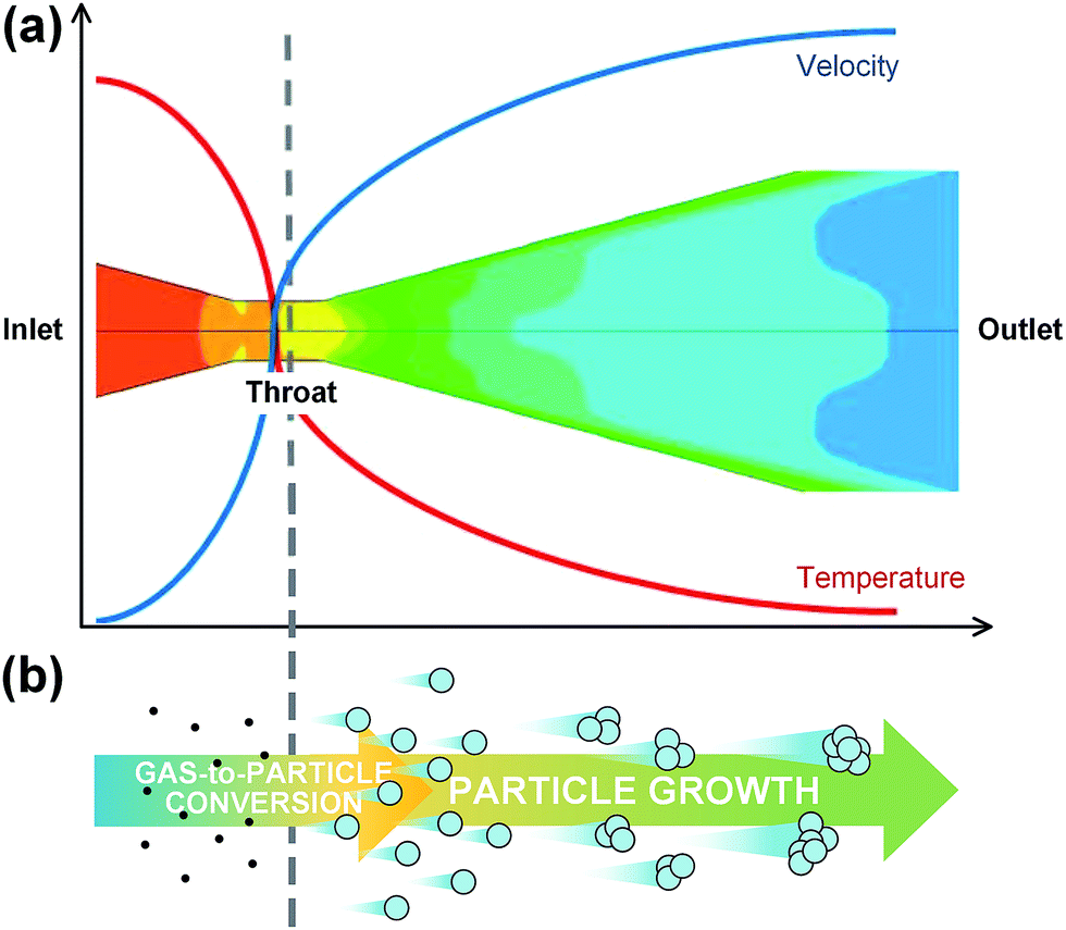 | ||
| Fig. 1 Diagrams for gas cluster generation by gas expansion through the converging–diverging nozzle. (a) Velocity and temperature profiles and pressure drop (colour contour) through the nozzle resulted by a rapid adiabatic expansion. (b) Gas cluster formation phenomena from gas-to-particle conversion to particle growth during the nozzle expansion. The produced clusters have great momenta with heavy mass and high velocity. | ||
Fig. 2 shows a schematic diagram and details of a CO2 gas cluster jet system with 9 nozzle arrays. It was designed to clean 300 mm wafer. The system was comprised of two vacuum cambers with desired mechanical systems which enable to transfer wafers from the loading chamber to the processing chamber and go back and forth for proper treatment scanning, low- and high-vacuum pumps, gas flow system, and nozzle control system. The nozzle arrays contained 9 nozzles with same geometry and they were tilted with fixed angle at 15°. A mechanical pump for low-vacuum pumping and a dry booster pump (GD4400) for higher vacuum level provided required vacuum condition for the processing chamber. Vacuum level for the processing chamber was around 0.2 Torr before the cluster generation and it arises to 0.3–0.4 Torr according to the gas introduction conditions. The nozzle temperature was controlled by an air-cooled chiller (MER630, DES) from −50 to −80 °C. There are several variables that affect the cluster generation in 300 mm wafer system, such as nozzle temperature, operating gas pressure (upstream/downstream), impaction angle, scanning time, and gap distance. During the process, operating gas pressure was changed by both CO2 flow rate and vacuum level of the process chamber. The number of scanning indicates how many times the wafer passed through the nozzle arrays with the moving speed of 2 mm s−1. Table 1 shows the experimental conditions used in this study.
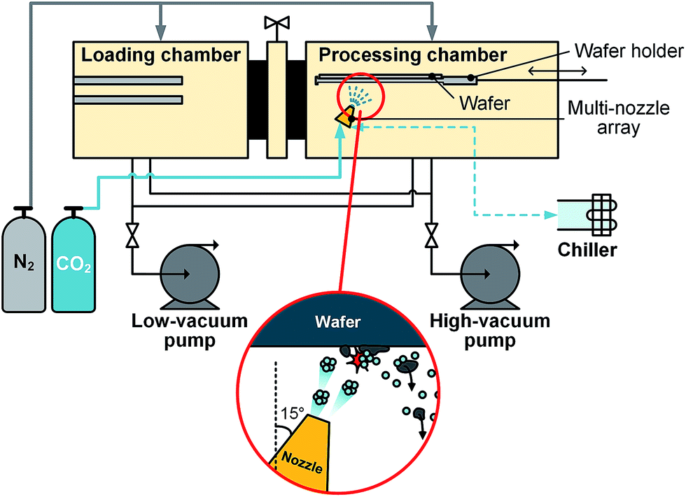 | ||
| Fig. 2 Schematic diagram and details of CO2 cluster cleaning equipment for 300 mm wafer cleaning. | ||
| Experimental conditions | Values |
|---|---|
| Gap distance (cm) (sample to nozzle exit) | 6 |
| CO2 flow rate (lpm) | 5/10/15 |
| Nozzle temperature (°C) | −50 |
| Number of scanning (times) | 1/4 |
| Angle of nozzle (°) | 15 |
| Scan speed (mm s−1) | 2 |
The improvement in the electrical property was checked by resistance measurement. For this, initially graphene was transferred on 500 μm gap Au electrodes deposited on SiO2/Si wafer. The current–voltage measurements were carried out between two Au electrodes using micro prober and semiconductor characterization system (SCS-4200, Keithley). To observe the difference between before and after cleaning, surfaces of the samples were analyzed by optical microscope (Olympus, BX51M-N35 MF). In addition, change of the surface morphology was also measured by atomic force microscope (AFM, Veeco Innova). Furthermore, Raman spectroscopy (WITec alpha300-R Raman spectroscope) analyses were performed under 532 nm-wavelength laser.
Measurement results of resistance were depicted in Fig. 3 as a bar chart. As a comparison, resistance was reduced from the pristine (non-treated) sample. 4 types of samples were compared with pristine graphene used sample. Samples, (1), (3), and (4), were treated with different flow rates under same other conditions (5, 10, 15 lpm at 6 cm gap distance, −50 °C nozzle temperature, 4 times of scanning no.). The sample (2) was tested under 10 lpm at 6 cm gap distance, −50 °C nozzle temperature with just one pass. The CO2 cluster treatments were conducted on 6 samples for each condition. The resistance variations were measured at 10 different locations on the samples. The reduction rates were about 31%, 77%, 81%, and 34%, for each sample (1)–(4) in Fig. 3. The cluster size that was generated at 10 lpm flow rate condition seemed to be optimal in removing defects on the graphene surface. Although there were differences in decrease amount, resistance reduction means superior surface cleanliness compared to non-treated graphene surface. It definitely indicated that the surface defects – inorganic, organic, etc.-on the graphene surface were removed by CO2 cluster treatment.
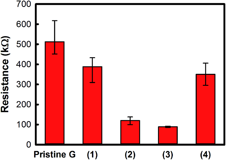 | ||
| Fig. 3 Resistance measurement results of pristine graphene, cluster treated graphenes with different conditions (gas flow rate/nozzle-to-sample gap distance/nozzle temperature/scanning frequency): (1) 5 lpm/6 cm/−50 °C/4, (2) 10 lpm/6 cm/−50 °C/1, (3) 10 lpm/6 cm/−50 °C/4, (4) 15 lpm/6 cm/−50 °C/4. | ||
To clarify the removal of defects, surface images of samples were compared using optical microscope (both bright field and dark field) as shown in Fig. 4. From the comparative results of non-treated graphene (a–c) and cluster treated graphene (d and e), it was observed that not only organic defects but also inorganic defects were efficiently removed. In general, CVD graphene has several surface defects which are described in Fig. 4(g); PMMA residues (organic defects), amorphous carbons, wrinkles, and foldings (inorganic defects). Organic contaminants removal by using CO2 gas cluster cleaning technology is well established. During treatment, cold CO2 gas clusters (∼−50 °C) impact and cause the thermal shock, resulting in to rapid shrinkage of organic contaminants and making their adhesion to the surface weaken.12 Eventually, the organic contaminants like PMMA residues detach from the substrate and are blown over by the CO2 gas cluster stream. For the inorganic surface defects on the CVD graphene, only the physical aspect can be considered. CO2 cluster jet cleaning technology deals with the adhesion and drag of contaminants so that the (contact) surface-to-volume (S/V) ratio are the key parameters. The contact area (S) to the substrate directly relates to the adhesion and the volume (V) enables to form sufficient drag forces by producing effective projection area. Accordingly, CO2 clusters jet directly impact on the graphene surface and selectively detach the surface defects by breaking the adhesion and blowing due to their minute S/V ratio while great S/V ratio of graphene.
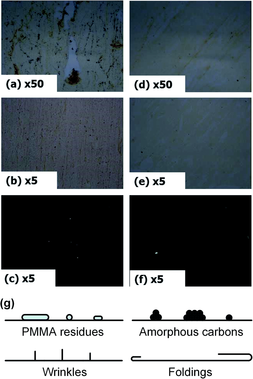 | ||
| Fig. 4 Optical microscope images of the surfaces by bright and dark field; non-treated surface images (a–c) and treated by clusters (d and f). (g) Conjectured controllable types of surface defects sorted into organic (PMMA residues) and inorganic (amorphous carbons, wrinkles, and foldings) defects. | ||
To evaluate the change in surface morphology of graphene samples before and after CO2 cluster treatment, AFM measurement were carried out and the results are described in Fig. 5. The overall roughness for each sample was found to be drastically reduced (by 42.3%) from 2.46 nm to 1.42 nm. These results were in agreement with the optical microscopic observations (Fig. 4); eliminations of the organic and inorganic surface defects on the graphene.
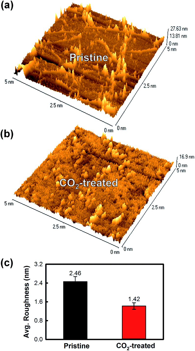 | ||
| Fig. 5 AFM analyses for the pristine and CO2-treated graphenes. Surface morphologies and heights for (a) pristine and (b) CO2-treated graphenes. (c) Change in the surface average roughness. | ||
Finally, Raman analyses were performed to evaluate the effects of CO2 cluster jet on the graphene crystallinity (Fig. 6). As shown in the Fig. 6(a), more crystal defects (identified by D band (∼1349.06 cm−1) and D′ band (∼1619.89 cm−1)) were induced after cleaning with CO2 cluster. It was comprehensible as that the CO2 clusters collide, detach the surface defects off and form vacancies or dangling bonds. Still there are debates going on the relationship between defects and the change is resistance. First of all, there are two types of crystal defects in graphene; point defects and line defects.13 Stone–Wales defects, single- and multiple vacancies, carbon adatoms, foreign adatoms, substitutional impurities, and topology of defective graphene are involved in point defects and dislocation-like defects such as grain boundaries and edges are concerned as line defects. All kinds of defects contribute to the D peak, and several efforts to quantifying defects by using Raman spectroscopy.14,15 In spite of point and line defects contribution to Raman spectra, the key factor to degrade electrical property of graphene is due to line defects only.16 Therefore, we could consider that the defects which occurred along with CO2 cluster jet treatment are point defects. This consideration is truly reasonable because graphene growth conditions were same for all samples so that the line defects, naturally formed and intrinsic, could not be controllable by the cluster treatment. Consequently, even though some point defects were formed by the treatment, the resistance was reduced by removing the surface defects. Though not only D band but also D′ band appeared for the CO2 cluster treated graphene due to its impaction, overall spectra involving G (∼1583.38 cm−1) and 2D (∼2684.76 cm−1) bands became intense resulted from the elimination of the surface defects. It is reasonable because that the participating high symmetry points (Γ, K and M) within the Brillouin zones of graphene can be released from the surface defects which had being suppressed them. Furthermore, those surface defects electromagnetically screen the Raman scattering resulting quenching of signal17 is in correlation with change in Raman intensities. Meanwhile, focusing on the G and 2D bands shifts which indicate the layer variation18 and chemical doping19 (Fig. 6(b)), CO2 cluster jet led the blue-shift of G band and red-shift of 2D band proposing a possibility of chemical doping or electronic energy band deformation and “mono-layerization”. To confirm this hypothesis, we need to perform more analyses.
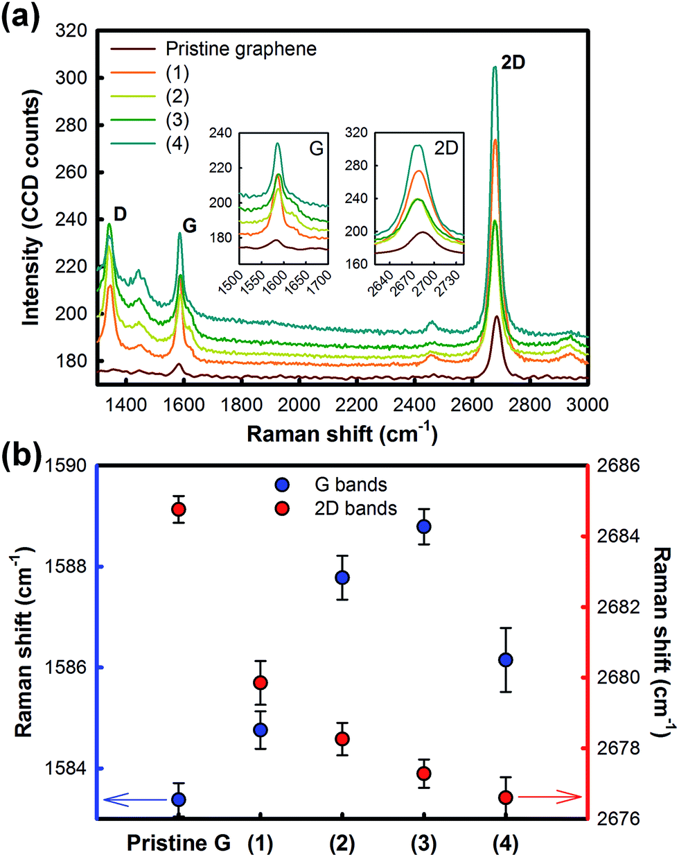 | ||
| Fig. 6 Raman analyses on the treatment conditions; (1)–(4) which in the order of increasing impact. (a) Raman spectra and (b) band position shifts of G and 2D bands. | ||
Conclusions
For the conditioning of graphene surface, removal of surface defects, such as polymeric residues and roughness factors, on the graphene was investigated by using CO2 cluster cleaning. The resistance was reduced from the pristine graphene sample with the reduction rates of 31%, 77%, 81%, and 34% for each sample. In addition, the comparison results of original graphene and cluster cleaned graphene measured by an optical microscopic and AFM confirmed the resistance results, which means that CO2 cluster cleaning decrease the roughness of surface with removal of surface defects. Finally, Raman spectroscopy results revealed that the overall phonon scattering increases with the blue-shift of G band and red-shift of 2D band after CO2 cluster cleaning. Therefore, more in-depth study is on-going to manifest the CO2 cluster impaction mechanism and effects on graphene surface. CO2 cluster cleaning has a potential to provide selective conditioning for graphene surface through fine tuning of cluster size and velocity.Acknowledgements
This work was partially supported by the National Research Foundation of Korea (NRF) (NRF-2013R1A1A2058893) and Basic Science Research Program through the National Research Foundation of Korea Grant funded by the Ministry of Science, ICT & Future Planning (2009-0083540).Notes and references
- X. Liang, B. A. Sperling, I. Calizo, G. Cheng, C. A. Hacker, Q. Zhang, Y. Obeng, K. Yan, H. Peng, Q. Li, X. Zhu, H. Yuan, A. R. H. Walker, Z. Liu, L.-m. Peng and C. A. Richter, ACS Nano, 2011, 5, 9144–9153 CrossRef PubMed.
- X. Li, W. Cai, J. An, S. Kim, J. Nah, D. Yang, R. Piner, A. Velamakanni, I. Jung, E. Tutuc, S. K. Banerjee, L. Colombo and R. S. Ruoff, Science, 2009, 324, 1312–1314 CrossRef CAS PubMed.
- S. Bae, H. Kim, Y. Lee, X. Xu, J.-S. Park, Y. Zheng, J. Balakrishnan, T. Lei, H. Ri Kim, Y. I. Song, Y.-J. Kim, K. S. Kim, B. Ozyilmaz, J.-H. Ahn, B. H. Hong and S. Iijima, Nat. Nanotechnol., 2010, 5, 574–578 CrossRef CAS PubMed.
- A. M. Goossens, V. E. Calado, A. Barreiro, K. Watanabe, T. Taniguchi and L. M. K. Vandersypen, Appl. Phys. Lett., 2012, 100, 073110–073113 CrossRef PubMed.
- C. W. Chen, F. Ren, C. Gou-Chung, S.-C. Hung, Y. P. Huang, J. Kim, I. I. Kravchenko and S. J. Pearton, J. Vac. Sci. Technol., B: Nanotechnol. Microelectron.: Mater., Process., Meas., Phenom., 2012, 30, 060604 CrossRef.
- Y.-D. Lim, D.-Y. Lee, T.-Z. Shen, C.-H. Ra, J.-Y. Choi and W. J. Yoo, ACS Nano, 2012, 6, 4410–4417 CrossRef CAS PubMed.
- Z. Cheng, Q. Zhou, C. Wang, Q. Li, C. Wang and Y. Fang, Nano Lett., 2011, 11, 767–771 CrossRef CAS PubMed.
- J. Moser, A. Barreiro and A. Bachtold, Appl. Phys. Lett., 2007, 91, 163513 CrossRef PubMed.
- C. R. Dean, A. F. Young, I. Meric, C. Lee, L. Wang, S. Sorgenfrei, K. Watanabe, T. Taniguchi, P. Kim, K. L. Shepard and J. Hone, Nat. Nanotechnol., 2010, 5, 722–726 CrossRef CAS PubMed.
- R. Jalilian, L. A. Jauregui, G. Lopez, J. Tian, C. Roecker, M. M. Yazdanpanah, R. W. Cohn, I. Jovanovic and Y. P. Chen, Nanotechnology, 2011, 22, 295705 CrossRef PubMed.
- H. Choi, H. Kim, D. Yoon, J. W. Lee, B.-K. Kang, M.-S. Kim, J.-G. Park, S.-B. Kwon and T. Kim, Microelectron. Eng., 2013, 102, 87–90 CrossRef CAS PubMed.
- C. W. Bowers, US Pat., 5,863,962, 1998 Search PubMed.
- F. Banhart, J. Kotakoski and A. V. Krasheninnikov, ACS Nano, 2010, 5, 26–41 CrossRef PubMed.
- L. G. Cançado, A. Jorio, E. H. M. Ferreira, F. Stavale, C. A. Achete, R. B. Capaz, M. V. O. Moutinho, A. Lombardo, T. S. Kulmala and A. C. Ferrari, Nano Lett., 2011, 11, 3190–3196 CrossRef PubMed.
- K. Niwase, Int. J. Spectrosc., 2012, 2012, 14 Search PubMed.
- H. S. Song, S. L. Li, H. Miyazaki, S. Sato, K. Hayashi, A. Yamada, N. Yokoyama and K. Tsukagoshi, Sci. Rep., 2012, 2, 337 CAS.
- Q. Zhou, S. Coh, M. L. Cohen, S. G. Louie and A. Zettl, Phys. Rev. B: Condens. Matter Mater. Phys., 2013, 88, 235431 CrossRef.
- D. Yoon, H. Moon, H. Cheong, J. S. Choi, J. A. Choi and B. H. Park, J. Korean Phys. Soc., 2009, 55, 1299–1303 CrossRef CAS.
- J. Yan, Y. Zhang, P. Kim and A. Pinczuk, Phys. Rev. Lett., 2007, 98, 166802 CrossRef.
Footnote |
| † These authors equally contributed to this work. |
| This journal is © The Royal Society of Chemistry 2014 |