A high-performance photovoltaic small molecule developed by modifying the chemical structure and optimizing the morphology of the active layer†
Wang Ni‡
,
Miaomiao Li‡,
Xiangjian Wan*,
Huanran Feng,
Bin Kan,
Yi Zuo and
Yongsheng Chen*
Key Laboratory of Functional Polymer Materials, Collaborative Innovation Center of Chemical Science and Engineering (Tianjin), Center for Nanoscale Science and Technology, Institute of Polymer Chemistry, College of Chemistry, Nankai University, Tianjin 300071, China. E-mail: yschen99@nankai.edu.cn; xjwan@nankai.edu.cn
First published on 9th July 2014
Abstract
A small molecule (DR3TDOBDT) containing 4,8-dioctyl benzo[1,2-b:4,5-b′]dithiophene as the central block and 3-(2-ethylhexyl)-rhodanine as the end-capping groups has been designed and synthesized. A power conversion efficiency of 8.26% was achieved through the active layer morphology optimization process combining thermal annealing and solvent vapor annealing.
Bulk heterojunction (BHJ) solar cells have attracted an increasing amount of attention due to their advantages of solution processability, low cost, light-weight, and flexibility.1 In the past few years, power conversion efficiencies (PCEs) above 9% have been achieved for polymer-based organic photovoltaic cells (P-OPVs).2 Meanwhile, more and more attention has been given to small molecule OPV cells (SM-OPVs) due to their competitive advantages in contrast to P-OPVs, such as a well-defined structure and therefore less batch-to-batch variation, easier band structure control, etc.3 Recently, great effort has focused on developing SM-OPVs and PCEs over 8% have been achieved through new molecule design and device optimization.4
To achieve commercialization of SM-OPVs, the PCE needs to be greatly improved. Generally, the design and synthesis of new small molecule materials and optimization of device fabrication are both important for improving the performance of SM-OPVs. The design and synthesis must consider several major issues: good solubility, broad optical absorption, suitable energy levels and high hole mobility. Optimization of device fabrication could be realized in many ways such as morphology control, interface engineering, device architecture and optical design.2a,d,5 Among these methods, morphology control is a fundamental and determining factor for achieving high performance OPVs. In view of these issues, structural modification of existing excellent small molecules and control of the morphology of the photoactive layer based on these new small molecule donor materials through different processing procedures would be an effective way to obtain high-performance SM-OPVs.
In our previous work, we have reported a small molecule, named DR3TBDT containing 2-ethylhexoxy-substituted benzo[1,2-b:4,5-b′]dithiophene (BDT) as the central building block. The OPV device based on DR3TBDT exhibits a high PCE of 7.38%, with an open-circuit voltage (Voc) of 0.93 V, a short-circuit current (Jsc) of 12.21 mA cm−2, and a fill factor (FF) of 65.0%.6 As we know, alkoxy chains show a stronger electron-donating ability than alkyl chains. Substituting bulky branched 2-ethylhexyloxy side chains with lower electron-donating octyl chains on BDT, could possibly achieve a deeper highest occupied molecular orbital (HOMO) energy level with a higher open circuit voltage (Voc) and better intermolecular packing.7 Thus, in this work, we designed and synthesised a new small molecule, named DR3TDOBDT (Scheme 1) containing an octyl substituted BDT as the central block and 3-(2-ethylhexyl)-rhodanine groups as the end-capping groups. Through primary optimization of photovoltaic performance, the OPV based on a DR3TDOBDT:PC71BM blend film shows an unsatisfactory PCE of 4.34%, with an indeed higher Voc of 0.98 V, but a lower Jsc of 8.52 mA cm−2, and a lower FF of 52.0%. Thermal annealing8 and solvent annealing9 including solvent vapor annealing, especially the first are effective approaches to fine tune the morphology of the active layer and thus improve the P-OPV performance. In an attempt to further improve the DR3TDOBDT-based device performance, we used a two-step annealing (TSA) approach involving thermal annealing and solvent vapor annealing to optimize the morphology of the photoactive layer. The PCE of the device base on a DR3TDOBDT:PC71BM blend film is significantly improved to 8.26% using the TSA approach, due to the much improved Jsc and FF while retaining the high Voc. These results indicate that the simple TSA approach could be used as an effective yet simple method to tune the morphology of the active layer for small molecule based devices.
 | ||
| Scheme 1 Chemical structure of DR3TDOBDT. | ||
The synthesis of DR3TDOBDT is outlined in Scheme S1 (ESI†). 2,6-Bis(trimethyltin)-4,8-dioctylbenzo[1,2-b:4,5-b′]dithiophene (1), 5-bromo-3,3-dioctyl-2,2′:5,2′′-terthiophene-2-carbaldehyde (2) and 3-(2-ethylhexyl)-rhodanine were prepared according to the literature.4b,7,10 DCHO3TDOBDT was synthesized using Stille coupling between 1 and 2. The target molecule, DR3TDOBDT was then prepared by Knoevenagel condensation of DCHO3TDOBDT with 3-(2-ethylhexyl)-rhodanine. The introduction of 2-ethylhexyl to replace ethyl on the rhodanine unit could improve the solubility of the target molecule and thus facilitate device fabrication. This new molecule exhibits good thermal stability up to 300 °C under N2 atmosphere (Fig. S1, ESI†).
The UV-Vis absorption spectra of DR3TDOBDT in chloroform and in the solid state are summarized in Table S1 (ESI†). As shown in Fig. 1a, DR3TDOBDT in diluted chloroform shows an absorption peak at 511 nm and a maximum absorption coefficient of 8.4 × 10⁴ M−1 cm−1. The DR3TDOBDT film cast from the chloroform solution shows a broader absorption and a red-shifted absorption peak at 583 nm with a maximum absorption coefficient of 6.5 × 104 cm−1. The DR3TDOBDT film shows a vibronic shoulder peak at 629 nm, indicating an effective π–π packing between the molecule backbones.11 The optical band gap of DR3TDOBDT is estimated to be 1.79 eV. The electrochemical properties of DR3TDOBDT were investigated using a cyclic voltammogram and the data are summarized in Table S1 (ESI†). As shown in Fig. 1b, the HOMO and lowest unoccupied molecular orbital (LUMO) energy levels, at −5.08 and −3.27 eV respectively, are calculated from the onset oxidation and reduction potential of the redox curves. The electrochemical band gap of DR3TDOBDT is estimated to be 1.81 eV, which is consistent with the optical band gap.
 | ||
| Fig. 1 (a) Absorption spectra of DR3TDOBDT in chloroform solution and in an as-cast film. (b) Cyclic voltammogram of DR3TDOBDT in dichloromethane solution of 0.1 mol L−1 Bu4NPF6 with a scan rate of 100 mV s−1. | ||
OPV cells were fabricated using DR3TDOBDT as the electron donor with a general device structure of indium tin oxide (ITO)/poly(3,4-ethylen-edioxythiophene) poly(styrenesulfonate) (PEDOT:PSS)/DR3TDOBDT:PC71BM/ZnO/Al using the conventional solution spin-coating process. The best result was observed for a donor–acceptor weight ratio of 1![[thin space (1/6-em)]](https://www.rsc.org/images/entities/char_2009.gif) :0.8 from chloroform solution with a donor concentration of 10 mg mL−1. The current density–voltage (J–V) curves of the OPV were recorded under 100 mW cm−2 simulated sunlight illumination. The typical results of the OPV devices with different treatments are given in Table 1 and Fig. 2b. The device based on a blend film without post treatment shows a PCE of 4.34%, with a Voc of 0.98 V, a Jsc of 8.52 mA cm−2, and a FF of 52.0%. Compared with the results of DR3TBDT, the device based on DR3TDOBDT indeed exhibits a higher Voc, which correlates with its lower HOMO energy level. The low Jsc and FF of the device are attributed to the unoptimized morphology of the DR3TDOBDT:PC71BM blend film, which could be seen from the TEM image (Fig. 3a) and will be discussed later. Here, we used a simple TSA approach combining thermal annealing and solvent vapor annealing to finely tune the morphology of the blend film, as shown in Fig. 2a. First, the DR3TDOBDT:PC71BM blend film as cast from the chloroform solution onto the PSS:PEDOT was heated on a hotplate at 75 °C for 10 minutes. After cooling to room temperature, the film was placed in a glass Petri dish containing 150 μL chloroform for solvent vapor annealing for 1 minute. The blend film was then removed and the ZnO layer and Al electrode were fabricated. For comparison, a device with only thermal annealing (TA) was fabricated and shows a PCE of 6.53%, with Voc of 0.96 V, Jsc of 11.34 mA cm−2 and FF of 60%. After the TSA process, the performance was significantly improved to a PCE of 8.26%, with Voc of 0.94 V, Jsc of 12.56 mA cm−2 and FF of 70%. The intermolecular interaction (or electronic coupling) between the donor and acceptor has great influence on the reverse dark saturation current density and thus Voc.12 Improving intermolecular interaction would decrease Voc. The strength of intermolecular interactions could be represented by Jso, which are 3.10 × 10⁻³, 8.21 × 10⁻³ and 1.11 × 10⁻¹ mA cm−2 for blend films without post treatment, with thermal annealing (TA) and TSA treatment, respectively (details in ESI†). The decreased Voc of blend films with TA and TSA treatment could be due to the increasing intermolecular interaction between the donor and acceptor.
:0.8 from chloroform solution with a donor concentration of 10 mg mL−1. The current density–voltage (J–V) curves of the OPV were recorded under 100 mW cm−2 simulated sunlight illumination. The typical results of the OPV devices with different treatments are given in Table 1 and Fig. 2b. The device based on a blend film without post treatment shows a PCE of 4.34%, with a Voc of 0.98 V, a Jsc of 8.52 mA cm−2, and a FF of 52.0%. Compared with the results of DR3TBDT, the device based on DR3TDOBDT indeed exhibits a higher Voc, which correlates with its lower HOMO energy level. The low Jsc and FF of the device are attributed to the unoptimized morphology of the DR3TDOBDT:PC71BM blend film, which could be seen from the TEM image (Fig. 3a) and will be discussed later. Here, we used a simple TSA approach combining thermal annealing and solvent vapor annealing to finely tune the morphology of the blend film, as shown in Fig. 2a. First, the DR3TDOBDT:PC71BM blend film as cast from the chloroform solution onto the PSS:PEDOT was heated on a hotplate at 75 °C for 10 minutes. After cooling to room temperature, the film was placed in a glass Petri dish containing 150 μL chloroform for solvent vapor annealing for 1 minute. The blend film was then removed and the ZnO layer and Al electrode were fabricated. For comparison, a device with only thermal annealing (TA) was fabricated and shows a PCE of 6.53%, with Voc of 0.96 V, Jsc of 11.34 mA cm−2 and FF of 60%. After the TSA process, the performance was significantly improved to a PCE of 8.26%, with Voc of 0.94 V, Jsc of 12.56 mA cm−2 and FF of 70%. The intermolecular interaction (or electronic coupling) between the donor and acceptor has great influence on the reverse dark saturation current density and thus Voc.12 Improving intermolecular interaction would decrease Voc. The strength of intermolecular interactions could be represented by Jso, which are 3.10 × 10⁻³, 8.21 × 10⁻³ and 1.11 × 10⁻¹ mA cm−2 for blend films without post treatment, with thermal annealing (TA) and TSA treatment, respectively (details in ESI†). The decreased Voc of blend films with TA and TSA treatment could be due to the increasing intermolecular interaction between the donor and acceptor.
:0.8, w/w) blend films with different post-treatments
 | ||
| Fig. 2 (a) Schematics of the TSA approach; (b). J–V curves of DR3TDOBDT:PC71BM (1:0.8, w/w) blend films with different post treatments. | ||
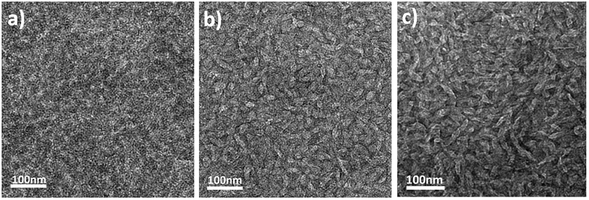 | ||
| Fig. 3 TEM images of DR3TDOBDT/PC71BM (1:0.8, w/w) blend films from CHCl3 with different post treatments. (a) Without treatment, (b) with TA and (c) with TSA treatment. | ||
X-ray diffraction (XRD) analysis was used to investigate order in the active layer for the devices without post treatment, with only TA treatment and with TSA treatment. As shown in Fig. S2 (ESI†), the DR3TDOBDT:PC71BM blend film shows a weak diffraction peak (100) at 2θ = 4.32°. For the blend film with TA treatment, a (100) diffraction peak at 2θ = 4.31° with significantly increased intensity was observed. Compared with the blend film with TA treatment, the blend film with TSA treatment shows a similar intensity diffraction peak (100) at 2θ = 4.35°. To demonstrate the influence of thermal annealing for the packing of DR3TDOBDT, the XRD analysis of pure DR3TDOBDT films with or without annealing were also investigated. As shown in Fig. S3 (ESI†), a DR3TDOBDT film with annealing shows better packing than a film without thermal annealing. The XRD results indicate that thermal annealing leads to the better organized assembly and crystallinity of DR3TDOBDT which would be of benefit for charge transport. As plotted in Fig. S4,† the hole mobilities of the DR3TDOBDT:PC71BM blend film through the hole-only device measured using the space charge limited current (SCLC) method are 3.44 × 10⁻⁵ cm2 V−1 s−1, 3.10 × 10⁻⁴ cm2 V−1 s−1 and 4.08 × 10⁻⁴ cm2 V−1 s−1 for blend films without post treatment, and with TA and TSA treatments, respectively. The hole mobilities of DR3TDOBDT:PC71BM blend films with TA and TSA treatments are an order of magnitude higher than for a film without any post treatment. The significantly higher hole mobilities of blend films with TA or TSA treatments are probably due to the better packing of DR3TDOBDT in the films, as observed from the above XRD data. The difference in hole mobilities between films with TA and TSA treatments could be related to morphology differences. To further understand this, transmission electron microscopy (TEM) and atomic force microscopy (AFM) were used to investigate DR3TDOBDT:PC71BM blend films with different treatments. As shown in Fig. S5,† blend films with different treatments have a relatively small root mean square (rms) roughness. The corresponding values are 0.70, 0.50 and 1.06 nm for films without post treatment, and with TA and TSA treatments, respectively. The TEM images clearly show the differences between the morphology of the blend films with different treatments. As shown in Fig. 3, the film without any post-treatment shows no obvious interpenetrating networks of the donor and acceptor phases. After TA treatment, crystal-like domains of size of 20–30 nm were observed. After the TSA treatment, the DR3TDOBDT:PC71BM blend films showed an interpenetrating network with width of 20 nm, which is comparable to the exciton diffusion length.13 The TEM results indicate that the simple TSA approach could finely tune the morphology of DR3TDOBDT:PC71BM blend films. The better morphology of blend films with thermal annealing and TSA treatment leads to increased donor–acceptor interfacial area and hole mobility, which could increase exciton dissociation and charge transport efficiency and reduce charge carriers recombination, and thus higher Jsc and FF.12a,14 Comprehensive studies on the TSA approach are in progress and will be discussed in a future publication.
In summary, a new A–D–A structure small molecule donor material DR3TDOBDT containing a benzo[1,2-b:4,5-b′]dithiophene as the central block unit and 3-(2-ethylhexyl)-rhodanine groups as the end-capping groups was designed and synthesized. This donor material indeed exhibits a higher open-circuit voltage, as designed, by using a less electron-donating group on the BDT unit. Using a simple TSA treatment, the BHJ device based on a DR3TDOBDT:PC71BM (1:0.8, w/w) blend gives a high PCE of 8.26%, with significantly improved short-circuit current and fill factor. These results also indicate that the TSA approach could be an efficient way to tune the morphology of the active layer for a small molecule system to produce better device performance.
Acknowledgements
The authors gratefully acknowledge the financial support from MoST (2014CB643502 and 2012CB933401), NSFC (51373078, 21374050 and 51273093), PCSIRT (IRT1257) and Tianjin city (13RCGFGX01121) and thank beam line BL14B1 (Shanghai Synchrotron Radiation Facility) for providing beam time.Notes and references
- (a) A. J. Heeger, Chem. Soc. Rev., 2010, 39, 2354–2371 RSC; (b) D. J. Lipomi and Z. Bao, Energy Environ. Sci., 2011, 4, 3314–3328 RSC; (c) F. He and L. Yu, J. Phys. Chem. Lett., 2011, 2, 3102–3113 CrossRef CAS; (d) Y. Lin, H. F. Dam, T. R. Andersen, E. Bundgaard, W. Fu, H. Chen, F. C. Krebs and X. Zhan, J. Mater. Chem. C, 2013, 1, 8007–8010 RSC; (e) H. Zhou, L. Yang and W. You, Macromolecules, 2012, 45, 607–632 CrossRef CAS.
- (a) Z. He, C. Zhong, S. Su, M. Xu, H. Wu and Y. Cao, Nat. Photonics, 2012, 6, 591–595 Search PubMed; (b) S.-H. Liao, H.-J. Jhuo, Y.-S. Cheng and S.-A. Chen, Adv. Mater., 2013, 25, 4766–4771 CrossRef CAS PubMed; (c) X. Guo, M. Zhang, W. Ma, L. Ye, S. Zhang, S. Liu, H. Ade, F. Huang and J. Hou, Adv. Mater., 2014, 26, 4043–4049 CrossRef CAS PubMed; (d) W. Zhang, Y. Wu, Q. Bao, F. Gao and J. Fang, Adv. Energy Mater., 2014 DOI:10.1002/aenm.201400359.
- (a) J. Roncali, Acc. Chem. Res., 2009, 42, 1719–1730 CrossRef CAS PubMed; (b) S. Shen, P. Jiang, C. He, J. Zhang, P. Shen, Y. Zhang, Y. Yi, Z. Zhang, Z. Li and Y. Li, Chem. Mater., 2013, 25, 2274–2281 CrossRef CAS; (c) C. M. Amb, S. Chen, K. R. Graham, J. Subbiah, C. E. Small, F. So and J. R. Reynolds, J. Am. Chem. Soc., 2011, 133, 10062–10065 CrossRef CAS PubMed; (d) A. Mishra and P. Bäuerle, Angew. Chem., Int. Ed., 2012, 51, 2020–2067 CrossRef CAS PubMed.
- (a) J. Zhou, Y. Zuo, X. Wan, G. Long, Q. Zhang, W. Ni, Y. Liu, Z. Li, G. He, C. Li, B. Kan, M. Li and Y. Chen, J. Am. Chem. Soc., 2013, 135, 8484–8487 CrossRef CAS PubMed; (b) Y. Liu, C.-C. Chen, Z. Hong, J. Gao, Y. Yang, H. Zhou, L. Dou and G. Li, Sci. Rep., 2013, 3, 3356 Search PubMed; (c) A. K. K. Kyaw, D. H. Wang, D. Wynands, J. Zhang, T.-Q. Nguyen, G. C. Bazan and A. J. Heeger, Nano Lett., 2013, 13, 3796–3801 CrossRef CAS PubMed.
- (a) G. Li, V. Shrotriya, J. Huang, Y. Yao, T. Moriarty, K. Emery and Y. Yang, Nat. Mater., 2005, 4, 864–868 CrossRef CAS; (b) W. Cao and J. Xue, Energy Environ. Sci., 2014, 7, 2123–2144 RSC.
- J. Zhou, X. Wan, Y. Liu, Y. Zuo, Z. Li, G. He, G. Long, W. Ni, C. Li, X. Su and Y. Chen, J. Am. Chem. Soc., 2012, 134, 16345–16351 CrossRef CAS PubMed.
- Y. Liang, D. Feng, Y. Wu, S.-T. Tsai, G. Li, C. Ray and L. Yu, J. Am. Chem. Soc., 2009, 131, 7792–7799 CrossRef CAS PubMed.
- (a) N. Camaioni, G. Ridolfi, G. Casalbore-Miceli, G. Possamai and M. Maggini, Adv. Mater., 2002, 14, 1735–1738 CrossRef CAS; (b) F. Padinger, R. S. Rittberger and N. S. Sariciftci, Adv. Funct. Mater., 2003, 13, 85–88 CrossRef CAS.
- (a) G. Li, Y. Yao, H. Yang, V. Shrotriya, G. Yang and Y. Yang, Adv. Funct. Mater., 2007, 17, 1636–1644 CrossRef CAS; (b) G. Lu, L. Li and X. Yang, Small, 2008, 4, 601–606 CrossRef CAS PubMed; (c) Z. Xiao, Y. Yuan, B. Yang, J. VanDerslice, J. Chen, O. Dyck, G. Duscher and J. Huang, Adv. Mater., 2014, 26, 3068–3075 CrossRef CAS PubMed.
- J. Zhou, X. Wan, Y. Liu, G. Long, F. Wang, Z. Li, Y. Zuo, C. Li and Y. Chen, Chem. Mater., 2011, 23, 4666–4668 CrossRef CAS.
- (a) Y. Matsuo, Y. Sato, T. Niinomi, I. Soga, H. Tanaka and E. Nakamura, J. Am. Chem. Soc., 2009, 131, 16048–16050 CrossRef CAS PubMed; (b) M.-C. Yuan, M.-Y. Chiu, S.-P. Liu, C.-M. Chen and K.-H. Wei, Macromolecules, 2010, 43, 6936–6938 CrossRef CAS.
- (a) C. W. Schlenker and M. E. Thompson, Chem. Commun., 2011, 47, 3702–3716 RSC; (b) K. Vandewal, K. Tvingstedt, A. Gadisa, O. Inganas and J. V. Manca, Nat. Mater., 2009, 8, 904–909 CrossRef CAS PubMed; (c) G. Long, X. Wan, B. Kan, Y. Liu, G. He, Z. Li, Y. Zhang, Y. Zhang, Q. Zhang, M. Zhang and Y. Chen, Adv. Energy Mater., 2013, 3, 639–646 CrossRef CAS.
- (a) C. M. Proctor, M. Kuik and T.-Q. Nguyen, Prog. Polym. Sci., 2013, 38, 1941–1960 CrossRef CAS PubMed; (b) X. Yang, J. Loos, S. C. Veenstra, W. J. H. Verhees, M. M. Wienk, J. M. Kroon, M. A. J. Michels and R. A. J. Janssen, Nano Lett., 2005, 5, 579–583 CrossRef CAS PubMed; (c) C. J. Brabec, N. S. Sariciftci and J. C. Hummelen, Adv. Funct. Mater., 2001, 11, 15–26 CrossRef CAS.
- B. Qi and J. Wang, Phys. Chem. Chem. Phys., 2013, 15, 8972–8982 RSC.
Footnotes |
| † Electronic supplementary information (ESI) available: Details of synthesis and characterization of DR3T(O-BDT), TGA, XRD, EQE, AFM, SCLC. See DOI: 10.1039/c4ra04862h |
| ‡ The first two authors contributed equally to this work. |
| This journal is © The Royal Society of Chemistry 2014 |