DOI:
10.1039/C4RA04853A
(Paper)
RSC Adv., 2014,
4, 46363-46368
Copper nanowire synthesis by directed electrochemical nanowire assembly†
Received
22nd May 2014
, Accepted 29th August 2014
First published on 29th August 2014
Abstract
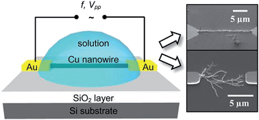
We present the growth of high aspect ratio copper nanowires with diameters of about 100 nm and a length of up to several micrometers via directed electrochemical nanowire assembly (DENA). We demonstrate that the nanowire morphology is controlled by the metal salt solution concentration and by the amplitude and frequency of the applied alternating voltage. The frequency was found to notably affect the nanowire diameter. The impact of the process parameters on the nanowire growth is discussed on the basis of the Butler–Volmer equation. The presented results for the bottom-up fabrication of copper wires are of high interest for nanosensor design, particularly for developing highly sensitive gas sensors. We suggest guidelines for the formation of copper nanowires based on experimental and theoretical considerations.
Introduction
The development of new cost efficient routes towards the fabrication of semiconducting and metallic nanowires is of great interest due to their growing impact and versatile application range in sensor technology and for designing novel electronic devices.1–8 For instance, copper interconnects play a particularly important role in nanoelectronics, because of its high electrical and thermal conductivity, low cost, and numerous potential applications in the micro- and nanotechnology industry, especially for electric power leads.9 Further potential applications include copper nanowire arrays as micropolarizer in optical devices,10 or copper nanowires as possible material for transparent electrodes as introduced by Rathmell and Zhang.11,12 Copper is biocompatible and allows the application of copper nanostructures as nanoprobes in biomedical devices13 and as biological sensors. Blondel et al.14 reported the electrodeposition of nanowires consisting of a succession of Cu and Co layers perpendicular to the wire axis. The wires exhibited a giant magnetoresistance, opening new prospects in magnetoelectronics.
Common methods for the fabrication of copper nanowires comprise template-based techniques usually with polycarbonate membranes15,16 or alumina templates.10,17–19 Wang et al. introduced the synthesis of copper nanotubes with silicon oxide nanowire templates by metal organic chemical vapour deposition (MOCVD).20 The authors fabricated a dense mat of entangled wires with this method. Other procedures for the synthesis of copper nanowires include hydrothermal reduction,11,21 vacuum vapour deposition,22 chemical vapour deposition,23 and electrodeposition.24 The main disadvantage of those bottom-up methods is the positioning and contacting of the nanowires after their synthesis.
Besides the bottom-up methods also top-down approaches can be used to fabricate copper nanowires, e.g. the damascene technology25 and e-beam lithography.26 However, the latter methods are usually complex and relatively expensive, involving multiple processing steps.
Many of the aforementioned applications of copper nanowires require the fabrication of thin and contacted wires. A promising method for this purpose is the synthesis of metal nanowires by directed electrochemical nanowire assembly (DENA).40 For this method, an alternating voltage is applied across a pair of electrodes in a metal salt solution, which induces the nucleation and growth of nanowires from one electrode to the other via the deposition of metal atoms at the growing nanowire tip.27,33,34,36 This one-step procedure allows the fast preparation of thin copper nanowires with large aspect ratios. As a consequence, the nanowires are already connected to the electrodes without the requirement for further processing (Fig. 1a). To our knowledge, this is the first report of copper nanowires synthesis by DENA.
 |
| Fig. 1 Schemes of the copper nanowire synthesis and the subsequent usage as gas sensor. (a) Experimental setup for copper nanowire growth from aqueous solution (not drawn to scale) between gold microelectrodes at a specific frequency f of the applied ac peak-to-peak voltage Vpp. (b) Schematic representation of a nanowire-based resistive sensor for gas sensing by means of oxidized copper nanowires. | |
In the present study, we explore the impact of process parameters, i.e. the solution concentration of the metal salt and the amplitude and frequency of the applied alternating voltage, on the resulting nanowire morphology and in particular on the nanowire diameter. The introduced preparation route is well suited to synthesize copper nanowires for a wide variety of applications. For example, the high surface-to-volume ratio of the thin wires makes them especially applicable for gas sensors. The concept of a resistive gas sensor based on copper oxide nanowires is shown schematically in Fig. 1b. The operation of semiconductor gas sensors is based on surface-chemical interactions between the gas molecules and the surface of the metal oxide. The interaction results in a change in the electrical resistance in the near-surface regions, which can be measured with high accuracy.
Our experimental findings concerning the impact of process parameters on the nanowire growth are discussed based on the Butler–Volmer equation. The theoretical considerations are helpful in understanding the processes during nanowire growth and allow establishing guidelines for achieving thin copper nanowires by the DENA synthesis.
Materials and methods
The experimental setup for the nanowire growth is illustrated in Fig. 1a. The wires were grown on an isolating substrate, using silicon wafers with a 400 nm oxide layer. The electrodes were fabricated by means of laser lithography (wavelength 405 nm, DWL66fs, Heidelberg Instruments). A layer of 3 nm chromium (for improved gold adhesion) was deposited on the developed structures followed by 20 nm gold evaporation. The gap between the electrodes was typically 10 μm. However, also electrodes with larger gaps up to 40 μm were used. 2.0 μl of aqueous copper(II)-nitrate (Cu(NO3)2, Sigma Aldrich) solutions with concentrations of 0.1, 0.5, 1.0, and 2.0 mM were dropped onto the electrode structure, as described in.18,28 After applying an ac voltage, nanowire growth was initiated on the substrate between the electrodes. A function generator (Tektronix AFG320) was used to provide a rectangular voltage signal in the frequency range from 50 kHz to 750 kHz, monitored by an oscilloscope (Tektronix TDS3014), with one electrode grounded. The electrodes were contacted by means of a tip-probing station (Karl Suss). The morphology of the grown nanowires was observed by scanning electron microscopy (SEM, Philips XL 30 ESEM-FEG). Elemental analysis was carried out with the same device using energy dispersive X-ray spectrometry (EDX) (ESI†). The SEM images of the nanowires allowed measuring the width and morphology of the nanowires from their top views. In the following, we refer to the width as nanowire diameter. The electrical wire properties were measured by a dual channel instrument (Keithley 2602 System SourceMeter).
Results
In our experiments, we varied the concentration c of copper ions in solution as well as the peak-to-peak voltage Vpp and frequency f of the applied ac voltage in order to elucidate their effect on the formation of copper nanowires. A fixed electrode gap size of 10 μm was chosen in these experiments. In the following, we present results of our analysis of the nanowire morphology, influenced by (i) salt concentration, (ii) amplitude, and (iii) frequency of the applied voltage.
Effect of salt concentration
The morphologies of nanowires grown at different cupric ion concentrations from 0.1 to 2.0 mM with a fixed voltage amplitude Vpp = 16 V and frequency f = 250 kHz are summarized in Fig. 2. Concentrations below 0.1 mM did not result in nanowire growth. At a concentration of 0.1 mM, the growth of thin and highly branched nanowires was observed with an average diameter of 65 nm (Fig. 2a). Further increase of the concentration led to the growth of thicker nanowires (Fig. 2c and d). Note that at concentrations of 1.0 and 2.0 mM, the wires are considerably less branched and for 2.0 mM the average diameter was 550 nm. The observed transition phenotypes from dendritic to more ordered patterns of wire morphology correlate well with the previous findings of Sawada et al. studying the electro-deposition of Zn.29
 |
| Fig. 2 SEM images of copper nanowires grown at concentrations of 0.1 (a), 0.5 (b), 1.0 (c), and 2.0 mM (d). Parameters: Vpp = 16 V, f = 250 kHz. Scale bars 5 μm. With higher concentrations the wires become thicker and less branched. | |
Effect of voltage amplitude
We have synthesized copper nanowires by applying peak-to-peak voltages of 6, 8, 10, and 20 V at a frequency of 250 kHz and a constant concentration of 1 mM (see Fig. 3). The voltage was turned off when the nanowires bridged the gap between the electrodes, detected by a sudden increase in current. Occasionally, the high current caused wire disruption due to melting or electromigration.30 This can be avoided by automatically switching off when the current exceeds a certain threshold or by using a resistor connected in series with the electrodes to limit the current flowing through completed nanowires.31,32 At the lowest applied voltage of 6 V, we did not observe bridging within an observation time of 3 min. The application of a higher voltage of 8 V induced the growth of a highly branched nanowire, which bridged the electrode gap. Further increase of the voltage to 10 and 20 V led to formation of less branched wires. At the highest tested voltage of 20 V, we also observed short nanowires growing at the electrode sides. The bridging nanowire in Fig. 3d has a diameter of approximately 450 nm. The other shown wires (Fig. 3a–c) are significantly thinner with diameters of about 120 nm. Note that the gold electrodes considerably dissolved at the tips during wire growth at 20 V.
 |
| Fig. 3 SEM images of copper nanowires grown at peak-to-peak voltages Vpp of 6 (a), 8 (b), 10 (c), and 20 V (d). Parameters: c = 1 mM, f = 250 kHz. Scale bars 5 μm. At a voltage of 6 V, the wire growth velocity is obviously too slow to connect the electrodes within 3 min observation time. | |
Effect of frequency
SEM images of copper nanowires grown at different frequencies from 50 to 750 kHz of the applied ac voltage of 8 V or 10 V and a concentration of 1 mM are shown in Fig. 4. It is worth noting that within an observation time of 3 min, no wire growth could be observed at the highest frequency of 750 kHz and a voltage of 8 V. For this frequency we increased the voltage to 10 V. The images in Fig. 4a–f demonstrate the trend that the nanowire diameters decrease with increasing frequency. The corresponding mean values and standard deviations of the wire diameters for each frequency are presented in Fig. 5. Each data point represents an average of 15 measurements on the corresponding SEM images. The mean diameters vary between 310 to 110 nm in the frequency range from 50 to 750 kHz, respectively. This trend is consistent with previous reports on DENA of indium and gold wires33 as well as platinum nanowires.34
 |
| Fig. 4 SEM images of copper nanowires grown at frequencies of 50 (a), 150 (b), 250 (c), 400 (d), 500 (e), and 750 kHz (f). Parameters: Vpp = 8 V (a–e), Vpp = 10 V (f), c = 1 mM. Scale bars 5 μm. The diameter of the wires decreases with increasing frequency. | |
 |
| Fig. 5 Wire diameter as a function of the frequency of the alternating voltage. The dotted line serves as a guide to the eye. | |
Electrical properties
After thorough analysis we were able to pinpoint an optimized set of process parameters (Vpp = 20 V, f = 250 kHz, c = 1 mM) to simultaneously grow single straight nanowires contacting one electrode tip to the other tip (Fig. 6). The distances between the electrodes were 40 μm. The I–V characteristics of the wires showed ohmic behaviour (ESI†). The average resistance of an intact wire was measured as 110 Ω. Assuming a cylindrical wire shape with 40 μm length and an average diameter of 300 nm, we can calculate a wire conductivity of 5 × 10⁶ S m−1. This value is approximately one order of magnitude lower than the conductivity of bulk copper of 5.96 × 10⁷ S m−1 at 20 °C.
 |
| Fig. 6 SEM images of three simultaneously grown copper nanowires with an electrode layout shown in the inset. Process parameters: Vpp = 20 V, f = 250 kHz, c = 1 mM. Scale bars 200 μm (left) and 10 μm (right). | |
A similar difference between nanosized and bulk materials was reported for Pd nanowires of about 200 nm diameter.27 It is very likely that the wire conductivity is diminished due to a polycrystalline structure and surface roughness (slight diameter variations).
Discussions
We have analysed the copper nanowire growth in dependency of experimental parameters (salt concentration, voltage, frequency). The observed copper nanowire assembly occurs by the reduction of copper ions at the electrode surface. |
Cu2+(aq.) + 2e− ⇔ Cu(s).
| (1) |
Electrons are transferred when the electrode is negatively charged during the negative half-cycle of the ac voltage. Reaction (1) is characterized by a standard electrode potential E°eq. of +0.34 V.35 According to the Nernst equation35
|
 | (2) |
the equilibrium potential
Eeq. for the lowest considered cupric ion concentration of 0.05 mM is about +0.21 V (approximating the activity by the concentration,
T – temperature,
z – ion charge number,
F – Faraday constant,
R – universal gas constant). Because of the applied alternating voltage, also dissolution of copper can happen at sufficiently high positive electrode potential. However, on average deposition predominates.
As a further reaction, reduction of hydrogen ions can occur
At the anode, the following oxidation reactions happen
|
2H2O ⇔ O2 + 4H+(aq.) + 4e−,
| (4) |
|
Au(s) ⇔ Au3+(aq.) + 3e−.
| (5) |
The standard electrode potentials for reactions (4) and (5) are +1.23 V and +1.5 V, respectively.35 The amplitudes of the rectangular voltage signals applied in our experiments (Vpp ≥ 6 V) are considerably larger than the above characteristic electrode potentials. Particularly clear evidence for the dissolution of the gold electrodes is given in Fig. 3d for a high voltage of Vpp = 20 V and to a less extent also in Fig. 2 at lower voltage. Dissolution of gold nano-dendrites has been comprehensively investigated elsewhere in ref. 43.
The nucleation of first copper precipitates on the gold surface obviously requires that the cupric ion concentration and the applied voltage amplitude exceed certain thresholds depending also on the frequency. For example, no nanowire assembly was observed within three minutes at a low concentration of 0.05 mM (Vpp = 16 V, f = 250 kHz) and at a low voltage of Vpp = 8 V (c = 1 mM, f = 750 kHz). The existence of such a voltage threshold was also reported for the DENA growth of indium wires.36 As a tendency, copper precipitation on gold should be supported by high cupric ion concentration at the electrode surface for negative electrode polarity. This near-surface concentration certainly increases with increasing bulk concentration. Moreover, due to cupric ion attraction during the negative half-wave of the voltage, the ion concentration is strongly enhanced. Higher voltage leads to larger electric field and correspondingly to larger attractive force. At lower frequency, the time for ion accumulation near the electrode surface is longer so that a higher concentration can be reached during one half-wave.
After formation of first copper precipitates, wires start to grow, where copper is now the electrode material. The charge transfer at the electrode surfaces for the deposition reaction (1) is commonly described by the Butler–Volmer equation37
|
 | (6) |
where
j is the charge current density across the electrode-electrolyte interface,
j0 the exchange current density,
E the electrode potential, and
Eeq. the equilibrium potential.
αa and
αc are the anodic and cathodic transfer coefficients. Negative values of the current (
j < 0) correspond to copper deposition. According to
eqn (6), the copper deposition rate strongly increases with increasing negative over-potential
E −
Eeq.. The equilibrium potential
Eeq. increases with the cupric ion concentration (
cf. eqn (2)), which facilitates copper deposition.
With increasing charge transfer rate at the wire surface, ion transport from the bulk solution to the wire via diffusion and field-driven migration will become rate-determining. This transport limitation is obviously the reason for the growth of the highly branched nanowires42 as seen for example in Fig. 2a and b. Such wire morphology greatly resembles the fractal structures obtained by diffusion-limited aggregation.38,41 The fractal dimension of copper electrodeposits grown under dc voltage has been shown41 to be in good agreement with computer simulations.
Ion transport driven by the electric field is particularly pronounced near the nanowire tip. Because of the small tip radius, the field strength at the tip can reach comparatively high values. Approximating the tip by a hemisphere of radius rtip and assuming a counter electrode in large distance ≫ rtip, the electric field in vacuum results as V/rtip at the tip surface, where V is the applied voltage. In the solution, the electric field is also affected by ion accumulation near the surface. This case has been analyzed in more detail for example in.39 The enhanced electric field at the nanowire tip leads to the preferred copper deposition at the tip.
For lower frequencies, ions are attracted for a longer time during one voltage pulse, leading to higher ion accumulation at the electrode surface even in wire surface regions exhibiting lower electric field strength. Thus, many thicker wires are formed as shown in Fig. 4a. Remarkably, wires start to grow on the whole gold electrode surface, not only at the electrode tip, as well as from both electrodes. With increasing frequency, only few wires are formed, preferably at the electrode tips. Generally, ion accumulation at the electrode surface becomes less with shorter voltage pulses. Since ion accumulation at the wire tip is largest (because of higher electric field), wires nearly exclusively elongate as seen for example in Fig. 4f. Note that if a wire is formed at one electrode, no wire forms at the other electrode. Branching of wires occurs presumably due to mass-transport limitation. The particularly fine wire structure in Fig. 2b suggests that, at relatively low bulk concentration of 0.1 mM, only thin wires can grow since only sufficiently small tip radius ensures a high enough electric field strength for copper deposition.
Fig. 6 demonstrates the controlled nucleation of the nanowire at sharp tips of the gold electrodes. In this case, the ion concentration of 1 mM and the frequency of 250 kHz were high enough to reduce the effect of mass-transport limitation as reason for wire branching. In this way, wires with only few short side branches and with wire diameters of about 300 nm could grow.
Conclusions
In this work, we demonstrated the controlled electrochemical synthesis of copper nanowires from an aqueous Cu(NO3)2 solution. This approach allows the rapid growth of copper nanowires with distinct morphologies at predefined electrode locations. Concluding from the experimental and theoretical investigations, we deduce the following guidelines to obtain thin nanowires:
• The electrode structures have to exhibit sharp tips for controlled nucleation sites to initiate nanowires growth.
• The frequency has to be adjusted above a threshold as such that the copper ion concentration at the nanowire tip is sufficiently high to ensure wire growth at the tip, but to avoid copper deposition on the other wire surface. The nanowire nucleation becomes harder at the initial gold electrode tips with increasing frequency, resulting in a lower ion accumulation at the electrode surfaces. Thus, the electrode tips should be as sharp as possible.
• In order to avoid wire branching, mass-transport limitation should be avoided by providing sufficiently large ion concentration.
• To prevent dissolution of the gold electrodes, it is of great importance to properly limit the voltage amplitude.
Further investigations will involve oxidation processes to transform grown copper nanowires into semiconducting CuO nanowires for gas sensor applications. The described synthesis method of copper nanowires presents a promising approach for a wide variety of further nanowire applications in the field of biosensorics.
Acknowledgements
This work is funded by the European Union (ERDF) and the Free State of Saxony via the ESF project 100098212 InnoMedTec. This research was supported by the European Union (ERDF) and the Free State of Saxony via TP A2 (“MolFunc”/“MolDiagnosik”). (0). We gratefully acknowledge support from the German Excellence Initiative via the Cluster of Excellence EXC 1056 “Center for Advancing Electronics Dresden” (cfAED).
Notes and references
- Y. Cui, Q. Wei, H. Park and C. M. Lieber, Science, 2001, 293, 1289–1292 CrossRef CAS PubMed.
- F. Favier, E. C. Walter, M. P. Zach, T. Benter and R. M. Penner, Science, 2001, 293, 2227–2231 CrossRef CAS PubMed.
- C. R. Martin, Science, 1994, 266, 1961–1966 CAS.
- Y. Xia, P. Yang, Y. Sun, Y. Wu, B. Mayers, B. Gates, Y. Yin, F. Kim and H. Yan, Adv. Mater., 2003, 15, 353–389 CrossRef CAS.
- A. Huczko, Appl. Phys. A, 2000, 70, 365–376 CrossRef CAS.
- E. C. Walter, R. M. Penner, H. Liu, K. H. Ng, M. P. Zach and F. Favier, Surf. Interface Anal., 2002, 34, 409–412 CrossRef CAS.
- F. M. Zörgiebel, S. Pregl, L. Römhildt, J. Opitz, W. Weber, T. Mikolajick, L. Baraban and G. Cuniberti, Nano Res., 2014, 7, 263–271 CrossRef.
- D. Nozaki and G. Cuniberti, Nano Res., 2009, 2, 648–659 CrossRef CAS.
- H. S. Virk, K. Kishore and V. Balouria, J. Nano Res., 2010, 10, 63–67 CrossRef CAS.
- Y. T. Pang, G. W. Meng, Y. Zhang, Q. Fang and L. D. Zhang, Appl. Phys. A, 2003, 76, 533–536 CrossRef CAS PubMed.
- A. R. Rathmell, S. M. Bergin, Y.-L. Hua, Z.-Y. Li and B. J. Wiley, Adv. Mater., 2010, 22, 3558–3563 CrossRef CAS PubMed.
- D. Zhang, R. Wang, M. Wen, D. Weng, X. Cui, J. Sun, H. Li and Y. Lu, J. Am. Chem. Soc., 2012, 134, 14283–14286 CrossRef CAS PubMed.
- X. Wen, Y. Xie, C. L. Choi, K. C. Wan, X.-Y. Li and S. Yang, Langmuir, 2005, 21, 4729–4737 CrossRef CAS.
- A. Blondel, J. P. Meier, B. Doudin and J. Ph. Ansermet, Appl. Phys. Lett., 1994, 65, 3019–3021 CrossRef CAS PubMed.
- M. Motoyama, Y. Fukunaka, T. Sakka, Y. H. Ogata and S. Kikuchi, J. Electroanal. Chem., 2005, 584, 84–91 CrossRef CAS PubMed.
- J.-L. Duan, J. Liu, H.-J. Yao, D. Moa, M.-D. Houa, Y.-M. Suna, Y.-F. Chena and L. Zhang, Mater. Sci. Eng., B, 2008, 147, 57–62 CrossRef CAS PubMed.
- G. A. Gelves, Z. T. M. Murakami, M. J. Krantz and J. A. Haber, J. Mater. Chem., 2006, 16, 3075–3083 RSC.
- H. Cao, L. Wang, Y. Qiu and L. Zhang, Nanotechnology, 2006, 17, 1736–1739 CrossRef CAS.
- G. Sharma, V. Kripesh, M. C. Simb and C. H. Sow, Sens. Actuators, A, 2007, 139, 272–280 CrossRef CAS PubMed.
- J. H. Wang, P. Y. Su, M. Y. Lu, L. J. Chen, C. H. Chen and C. J. Chu, Electrochem. Solid-State Lett., 2005, 8, C9–C11 CrossRef CAS PubMed.
- M. Mohl, P. Pusztai, A. Kukovecz and Z. Konya, Langmuir, 2010, 26, 16496–16502 CrossRef CAS PubMed.
- Z. Liu and Y. Bando, Adv. Mater., 2003, 15, 303–305 CrossRef CAS.
- H. Choi and S.-H. Park, J. Am. Chem. Soc., 2004, 126, 6248–6249 CrossRef CAS PubMed.
- E. C. Walter, M. P. Zach, F. Favier, B. J. Murray, K. Inazu, J. C. Hemminger and R. M. Penner, ChemPhysChem, 2003, 4, 131–138 CrossRef CAS PubMed.
- W. Steinhögl, G. Schindler, G. Steinlesberger, M. Traving and M. Engelhardt, J. Appl. Phys., 2005, 97, 023706 CrossRef PubMed.
- Q. Huang, C. M. Lilley, M. Bode and R. Divan, J. Appl. Phys., 2008, 104, 023709 CrossRef PubMed.
- C. Cheng, R. K. Gonela, Q. Gu and D. T. Haynie, Nano Lett., 2005, 5, 175–178 CrossRef CAS PubMed.
- A. Nerowski, J. Opitz, L. Baraban and G. Cuniberti, Nano Res., 2013, 6, 303–311 CrossRef CAS.
- Y. Sawada, A. Dougherty and J. P. Gollub, Phys. Rev. Lett., 1986, 56, 1260–1263 CrossRef CAS.
- D. R. Strachan, D. E. Smith, M. D. Fischbein, D. E. Johnston, B. S. Guiton, M. Drndić, D. A. Bonnell and A. T. Johnson, Jr, Nano Lett., 2006, 6, 441–444 CrossRef CAS PubMed.
- A. Nerowski, M. Poetschke, M. Bobeth, J. Opitz and G. Cuniberti, Langmuir, 2012, 28, 7498–7504 CrossRef CAS PubMed.
- B. C. Gierhart, D. G. Howitt, S. J. Chen, R. L. Smith and S. D. Collins, Langmuir, 2007, 23, 12450–12456 CrossRef CAS PubMed.
- B. Ozturk, I. Talukdar and B. N. Flanders, Nanotechnology, 2007, 18, 365302 CrossRef.
- J. K. Kawasaki and C. B. Arnold, Nano Lett., 2011, 11, 781–785 CrossRef CAS PubMed.
- CRC Handbook of Chemistry and Physics, ed. W. M. Haynes, Taylor and Francis Group, Boca Raton, 94th edn, 2014, vol. 1 Search PubMed.
- I. Talukdar, B. Ozturk, B. N. Flanders and T. D. Mishima, Appl. Phys. Lett., 2006, 88, 221907 CrossRef PubMed.
- W. Schmickler and E. Santos, Interfacial Electrochemistry, Springer-Verlag Berlin Heidelberg, 2010 Search PubMed.
- T. A. Witten and L. M. Sander, Phys. Rev. Lett., 1981, 47, 1400–1403 CrossRef CAS.
- M. Poetschke, M. Bobeth and G. Cuniberti, Langmuir, 2013, 29, 11525–11534 CrossRef CAS PubMed.
- B. Ozturk, B. N. Flanders, D. R. Grischkowsky and T. D. Mishima, Nanotechnology, 2007, 18, 175707 CrossRef.
- R. M. Brady and R. C. Ball, Nature, 1984, 309, 225–229 CrossRef CAS.
- A. Nerowski, M. Poetschke, U. Wiesenhuetter, J. Nikolai, U. Cikalova, A. Dianat, A. Erbe, J. Opitz, M. Bobeth, L. Baraban and G. Cuniberti, Langmuir, 2014, 30(19), 5655–5661 CrossRef CAS PubMed.
- G. Paneru and B. N. Flanders, Nanoscale, 2014, 6, 833–841 RSC.
Footnotes |
† Electronic supplementary information (ESI) available. See DOI: 10.1039/c4ra04853a |
‡ These authors contributed equally to this work. |
|
This journal is © The Royal Society of Chemistry 2014 |
Click here to see how this site uses Cookies. View our privacy policy here.