DOI:
10.1039/C4RA04828H
(Paper)
RSC Adv., 2014,
4, 27084-27090
Cabbage leaf-shaped two-dimensional TiO2 mesostructures for efficient dye-sensitized solar cells
Received
24th April 2014
, Accepted 10th June 2014
First published on 12th June 2014
Abstract
We have fabricated ‘cabbage leaf’-like TiO2 mesostructures of high surface area from electrospun TiO2–SiO2 composite nanofibers by titanate route for dye-sensitized solar cell (DSC) application. The initial TiO2–SiO2 composite nanofibers, the intermediate titanate and the final leaf-like TiO2 are characterized by spectroscopy, microscopy and surface area measurements. The material (final TiO2) acts as a dual functional material in DSCs with high dye loading and a high light scattering capability. The best DSC (a square-shaped cell of area 0.20 cm2 and thickness of 12 μm) fabricated out of the material showed a superior photovoltaic performance with an efficiency (η) of 7.92% in comparison to that of commercial P25 TiO2 (6.50%).
Introduction
The pioneering work of O'Regan and Grätzel on dye-sensitized solar cells (DSCs) created a new outlook to solar energy conversion technology which integrated different fields of science.1 Titanium dioxide (TiO2) is a versatile and widely used material which has applications in different fields such as photovoltaics, storage devices, photocatalytic water splitting, electrochromic devices, self-cleaning coatings, environmental remediation, etc.2–13 TiO2 forms the backbone of the DSCs as it performs the dual functions of supporting the sensitizers (dyes) and transporting the photoinjected electrons to the back contact. The high surface area, smooth charge transport properties (high crystallinity and/or one/two/three-dimensionality) and high light scattering capability of TiO2 are vital parameters in deciding the photovoltaic performance of DSCs. With these views in mind, different nanostructures have been developed in the past two decades such as nanoparticles,14–16 nanowires,17–19 nanotubes,20–22 nanobelts,23,24 nanospindles,25 nanofibers, etc.26,27 for DSC applications. Except the spherical nanoparticles, all others generally fit into the category of one-dimensional (1-D) nanostructures.
Though there are several methodologies around for the fabrication of 1-D TiO2, electrospinning is a versatile technique for fabricating TiO2 in the 1-D form of nanofibers.28,29 The TiO2 nanofibers are very good at light scattering as well as in providing a guided/semi-guided electron transport to the back contact. But these materials have shown low conversion efficiency (∼4–5%) due to their low internal surface area and hence poor dye-loading.30–34 Thus we thought of ways to enhance the surface area of electrospun TiO2 to have superior DSC performance. The titanate route which is the chemical transformation of spherical TiO2 nanoparticles into wires/rods by the action of conc. NaOH (first reported by Kasuga et al.35,36) was adopted for the purpose as we recently found that the same methodology can produce flower/leaf-shaped TiO2 from TiO2–SiO2 composite nanofibers (the purpose of preparing the composite fibers of TiO2–SiO2 was that the SiO2 can be dissolved by NaOH during the titanate process and etching of SiO2 from TiO2–SiO2 composite leads to enhanced surface area for the TiO2).37,38 The flower-shaped material showed excellent photocatalytic properties, however, the photovoltaic property of the TiO2 was not explored which is the subject matter of the present paper. The initial TiO2–SiO2 composites, the intermediate sodium titanate and the final leaf-shaped TiO2 were characterized by spectroscopy, microscopy and BET surface area measurements. A dye-sensitized solar cell (0.2 cm2 area, square-shaped, 12 μm thick) fabricated from the leaf-shaped TiO2 showed an efficiency of 7.92% when tested under AM1.5G conditions. The cell also showed an incident photon-to-electron conversion efficiency maximum of 79% at 532 nm.
Experimental
a. Materials
PVP (polyvinylpyrrolidone, Mw = 1.3 × 10⁶, mp. 300 °C, Aldrich, Steinhseim, Germany), methanol (Aldrich, Steinhseim, Germany), acetic acid (LR, Nice Chemicals, India), titanium(IV) isopropoxide (TiP, 97%, Aldrich, Germany), tetraethoxysilane (TES, 98% GC grade, Alfa Aesar, UK), sodium hydroxide pellets (A.R, Nice Chemicals, India), hydrochloric acid (ACS, ISO Reag. Ph Eur, Merk KGaA, Germany), N719 dye (Solaronix SA), fluorine-doped tin oxide plates (FTO, sheet resistance of 6–8 Ω □−1 fabricated in-house by spray pyrolysis deposition method) were used as such. The precursors of the FTO solution were made of dibutyltin diacetate (DBTDA) in 2-propanol (0.2 M) and ammonium fluoride (NH4F) in water (9 M).
b. Preparation of cabbage leaf-like TiO2 mesostructures
Cabbage leaf-like (CL) TiO2 mesostructures were synthesized from electrospun TiO2–SiO2 composite nanofibers. The solution for electrospinning was made by dissolving 0.6 g PVP in 14 mL of methanol. This was followed by the addition of 4 mL of acetic acid (99.7%), 1.75 mL of titanium(IV) isopropoxide and 0.25 mL of tetraethoxysilane, respectively. The mixture was stirred for 12 h to have sufficient viscosity for electrospinning. The mixture was electrospun at 20 kV with a flow rate of 0.5 mL h−1 using a climate controlled electrospinning unit (IME Technologies, The Netherlands). The distance between the needle tip and the static collector (covered with an Al foil) was about 10 cm. The humidity level inside the electrospinning chamber was maintained at ∼50%. The as-spun nanocomposite peeled-off from the Al foil in the form of a white sheet was annealed at 450 °C for 3 h for polymer degradation and crystallization of the TiO2–SiO2 composite. The TiO2–SiO2 composite obtained in the form of white flakes was analyzed by microscopy to confirm the nanofiber morphology of the composite.
About 600 mg of electrospun TiO2–SiO2 composite nanofibers was chemically treated in excess of concentrated sodium hydroxide (5 M NaOH) at 180 °C for 24 h in a Teflon-lined steel autoclave to chemically transform the nanocomposite into titanates with the in situ etching of SiO2 completely. The fluffy white titanate was collected and washed repeatedly with Millipore water to have pH = 7 for the washed solution. The titanate was subsequently soaked in dil. hydrochloric acid (0.1 M HCl) for 24 h and again washed repeatedly with Millipore water and dried at 180 °C for 30 min. During the acid treatment and subsequent drying process, the sodium titanate gets converted into hydrogen titanate and finally into TiO2. The TiO2 was characterized by spectroscopy, microscopy and BET surface area measurements.
c. Characterization of the TiO2–SiO2 composite, the titanate and the leaf-like TiO2 material
The annealed TiO2–SiO2 nanofibers and the leaf-like TiO2 were characterized by spectroscopy, microscopy and surface area measurements. The scanning electron microscopy (SEM) was performed by a JSM 6490 LA (JEOL-Tokyo, Japan) machine at an operating voltage at 15 kV. A thin film of gold was sputtered on the material using a sputter coating machine (JEOL-Tokyo, Japan). UV-visible spectra of the TiO2 thin films (in diffuse-reflectance mode) were measured by a Varian Cary 5000 spectrometer. Transmission Electron Microscopy (TEM) (SEI Tecnai G230) was also carried out for high-resolution imaging. Brunauer–Emmett–Teller (BET) surface area analyzer (Tristar II 3020 Surface Area Analyzer, Micromeritics, USA) was used to analyze the surface area and pore size of the samples, respectively under standard protocol. The powder XRD was performed by an X'pert pro PAN Analytical operated at a data interval of 0.03° and a current of 30 mA with a voltage of 40 KV. X-ray photoelectron spectroscopy (XPS, Kratos Analytical, UK) and Raman spectroscopy (Witec confocal Raman-300 AR instrument using an excitation laser of 488 nm wavelength and power of 0.6 μW, the spot size was >2 μm) were carried out according to standard procedures.
d. Fabrication of dye-sensitized solar cells (DSCs)
The polyester used to make a paste of TiO2 was made according to a reported procedure by the polycondensation of citric acid and ethylene glycol at 100 °C.31 About 100 mg of the TiO2 was mixed with 100 μL of the polyester and sonicated for ∼12 h to get a paste of the right rheology necessary for doctor blading. This was screen-printed/doctor-bladed on FTO plates which already had a blocking layer (80 nm thick) of TiO2 deposited by spray pyrolysis deposition of a TiO2 colloid (consisting of ∼5 nm size particles). The TiO2 paste was doctor-bladed on FTOs at different thicknesses ranging from 14 μm to 20 μm. The P25 was also doctor-bladed similarly for a comparative study. The doctor-bladed films were sintered at 450 °C for 1 h for removal of the polymer. The porous TiO2 films had thicknesses ranging from 12 μm to 18 μm. The porous films were subsequently treated with aq. TiCl4 solution (30 mM, 70 °C) for 30 min and sintered at 450 °C for 1 h. The TiO2 electrodes were immersed in N719 dye solution (0.5 mM in 1![[thin space (1/6-em)]](https://www.rsc.org/images/entities/char_2009.gif) :1 acetonitrile-tert-butanol mixture) at room temperature for 24 h. The weakly adsorbed dyes were removed by washing the electrodes in absolute acetonitrile. Platinum (Pt) sputter-coated FTO was used as the counter electrode. The active area of dye-sensitized TiO2 was about 0.20 cm2. The electrodes were sealed with a UV curable sealant and filled with I3−/I− electrolyte (in which, acetonitrile was used as solvent) by vacuum back-filling process using an electrolyte filling robot (SPD Inc. Laboratory, Japan). I–V characteristic of the DSCs was measured by a solar simulator under AM1.5G condition (Newport Oriel class A-Solar simulator, USA). The incident photon-to-current conversion efficiency (IPCE) was measured using an Oriel Newport (QE-PV-SI/QE) IPCE Measurement kit, USA.
:1 acetonitrile-tert-butanol mixture) at room temperature for 24 h. The weakly adsorbed dyes were removed by washing the electrodes in absolute acetonitrile. Platinum (Pt) sputter-coated FTO was used as the counter electrode. The active area of dye-sensitized TiO2 was about 0.20 cm2. The electrodes were sealed with a UV curable sealant and filled with I3−/I− electrolyte (in which, acetonitrile was used as solvent) by vacuum back-filling process using an electrolyte filling robot (SPD Inc. Laboratory, Japan). I–V characteristic of the DSCs was measured by a solar simulator under AM1.5G condition (Newport Oriel class A-Solar simulator, USA). The incident photon-to-current conversion efficiency (IPCE) was measured using an Oriel Newport (QE-PV-SI/QE) IPCE Measurement kit, USA.
e. Electrochemical impedance spectroscopy (EIS) of the DSCs
The electron lifetime and recombination resistance of DSCs were studied using EIS under dark with an applied bias voltage of 0.69 V. In EIS the current response of the cell by applying a small sine wave perturbation was evaluated by using an Autolab (Metrohm, Newport model, Netherlands).
Results and discussion
a. Characterization of as-electrospun nanofibers, sintered nanocomposite and the leaf-shaped TiO2
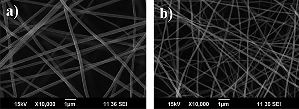
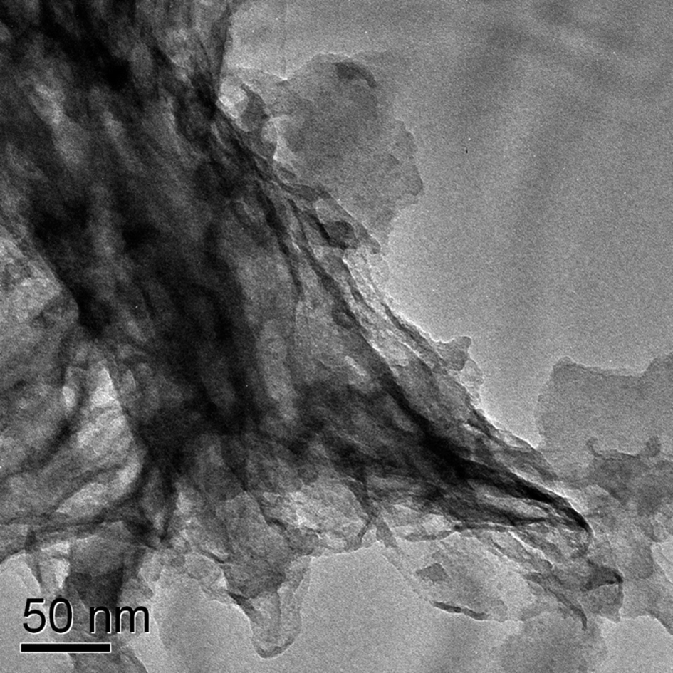
A SEM image of the as-electrospun TiO2–SiO2–PVP composite nanofibers is shown in Fig. 1a. The fibers were smooth and nearly continuous with diameters ranging from 250–300 nm. The as-electrospun nanofibers were sintered at 450 °C for 3 h to obtain TiO2–SiO2 composite nanofibers with an average diameter of 150 nm (Fig. 1b). The reduction in the fiber diameter is due to the degradation of polymer from the composite matrix. Fig. 2a shows a large area TEM image of the TiO2–SiO2 composite fibers. Fig. 2b shows a magnified TEM image of a single nanofiber. The high-resolution TEM image (Fig. 2c) indicates the presence of amorphous SiO2 and anatase TiO2. The anatase phase of TiO2 in composite was established by the characteristic lattice spacing of 0.35 nm corresponding to the (101) lattice of anatase (high resolution TEM image in Fig. 2c). The areas (marked in circles) in Fig. 2c indicate the distribution of amorphous SiO2 in the TiO2–SiO2 fibers. The selected area electron diffraction (SEAD) pattern of the TiO2–SiO2 nanofibers (Fig. 2d) shows polycrystallinity of the composite.
 |
| | Fig. 1 SEM images of (a) as-spun TiO2–SiO2–PVP fibers and (b) TiO2–SiO2 nanofibers formed after annealing at 450 °C. | |
 |
| | Fig. 2 TEM images of (a) electrospun TiO2–SiO2 nanofiber, (b) a magnified image of single nanofiber (c) high-resolution TEM of the TiO2–SiO2 nanofiber where unresolved portion shows amorphous SiO2 and anatase TiO2 with lattice spacing of 0.35 nm in the composite and (d) SAED pattern shows polycrystallinity of the composite. | |
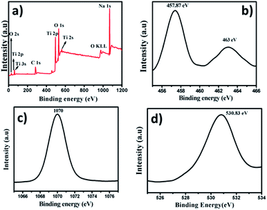
The TiO2–SiO2 composite was further analyzed by powder XRD, BET surface area and XPS measurements, respectively. The prominent peaks in the powder XRD spectrum (indexed in the spectrum itself) of the material confirm the anatase nature of the TiO2 and amorphous nature of SiO2 in the composite (Fig. 3a, peaks corresponding to the SiO2 were absent further confirming its amorphous nature). The presence of Si in the composite was confirmed by energy dispersive X-ray spectrum, EDS (Fig. 3b). The BET surface area of the TiO2–SiO2 composite nanofibers was measured to be 32 m2 g−1. The XPS survey spectrum showing the elemental composition of the composite material is shown in Fig. 4a and the resolved spectra of the elements are shown in Fig. 4b–d. The binding energies for Ti 2p3/2 and Ti 2p1/2 were centered at 452.09 eV and 457.85 eV, respectively (Fig. 4b) that corresponds to a spin–orbit coupling of 5.76 eV. In Fig. 4c, the O 1s peak could be de-convoluted into 2 peaks at 528.17 eV, 532.68 eV, respectively, corresponding to the O atom in Ti–O–Ti and Ti–O–Si bonds.38 Thus, the XPS spectrum indicates the incorporation of SiO2 in the TiO2 matrix through Ti–O–Si bonds. The Si peak in the high resolution spectrum (Fig. 4d) is centered at a binding energy 97.61 eV.
 |
| | Fig. 3 (a) Powder XRD spectrum and (b) EDS spectrum of the TiO2–SiO2 composite. The Au signal is from the sputter coating. | |
 |
| | Fig. 4 (a) XPS wide spectrum of TiO2–SiO2 composite and high resolution spectrum of (b) Ti (c) oxygen (d) Si. | |
The TiO2–SiO2 composite obtained by the sintering process upon NaOH treatment results in conversion of TiO2 into sodium titanate (Na2Ti3O7) with the in situ dissolution of SiO2. The strong diffraction peak at 2θ = 10° in XRD (Fig. 5) indicates the complete conversion of the composite into titanate.39 The XPS spectrum of material (Fig. 6a) after the NaOH treatment (the titanate) confirms complete etching of SiO2 and the formation of sodium titanate. The binding energies obtained from high resolution spectra of Ti 2p3/2 (centered at 457.87 eV) and Ti 2p1/2 (centered at 463 eV) reveals that Ti is in a different chemical environment than that of TiO2 (Fig. 6b). The single peak for O 1s at 530.83 eV represents the O in the Ti–O–Ti bonds (Fig. 6d).40 The Na 1s peak is obtained at a binding energy of 1072 eV (Fig. 6c). TEM image of the Na2Ti3O7 indicated the presence of layered sheet-like structures as evident from Fig. 7.37,40 The layered and porous nature contributed to a high surface area of 200 m2 g−1 for the titanate.
 |
| | Fig. 5 Powder XRD spectrum of sodium titanate showing a strong peak around 2θ = 10°. The peaks are indexed in the spectrum itself (JCPDS file no. 72-0148). | |
 |
| | Fig. 6 (a) XPS wide spectrum showing complete etching of SiO2 and presence of Na in the sample. High resolution spectrum of (b) Ti, (c) Na and (d) O. | |
 |
| | Fig. 7 TEM image of the sodium titanate formed indicating the presence of layered sheet-like structures. | |
Further acid treatment and low temperature sintering resulted in the formation of cabbage leaf-like TiO2 (SEM images in Fig. 8a and b, respectively) possibly through a self-assembly of the sheet-like structures.37 The BET surface area of the TiO2 was about 132 m2 g−1. High resolution TEM image of a part of the leaf-like structure is shown in Fig. 8c which confirms that the leaf-like TiO2 is actually made-up of small spherical particles of 10–20 nm sizes. The SAED image (inset of Fig. 8c) reveals the high polycrystallinity of the TiO2. The lattice-resolved TEM image of the TiO2 confirms its anatase structure (lattice spacing of 0.35 nm corresponds to the (101) orientation of the anatase TiO2). Fig. 9a shows the XRD pattern of the leaf-like TiO2 showing it's crystalline and anatase nature. The peaks are indexed in the spectrum itself. The particle size estimated from the full-width at half maximum of the (101) peak using the Debye Scherrer formula was ∼12 nm which is in close agreement with the HR-TEM results in Fig. 8c and d. The XPS spectroscopy was also used to confirm elemental composition and phase purity of the TiO2 (wide spectrum in Fig. 9b). The binding energies of Ti 2p3/2 and Ti 2p1/2 were centered at 456.48 eV and 462.16 eV, respectively (Fig. 9c) corresponding to a spin–orbit coupling of 5.68 eV. The single peak obtained at 527.75 eV for O 1s (Fig. 9d) further confirms the absence of SiO2 related impurities in the final product implying the complete removal of SiO2 from TiO2–SiO2 composite by the action of alkali.
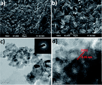 |
| | Fig. 8 (a) and (b) SEM image of cabbage leaf-like TiO2 at different resolutions (c) HRTEM showing that each petal is composed of nanoparticles of diameter 10–20 nm. (d) HRTEM showing the lattice spacing of TiO2. | |
 |
| | Fig. 9 (a) Powder XRD of leaf shaped TiO2 (b) XPS Survey spectrum and high resolution XPS spectra of (c) titanium and (d) oxygen of the TiO2. | |
The Raman spectrum of the TiO2 in Fig. 10 shows the major peaks of anatase TiO2. The peaks at 404 cm−1 and 527 cm−1 correspond to the Bg1 and Ag1 vibrational modes, respectively. The other peaks (165 cm−1, 207 cm−1 and 648 cm−1) observed in the Raman spectrum corresponds to the Eg vibrational mode.41
 |
| | Fig. 10 Raman spectrum of the leaf-shaped TiO2. | |
b. Photovoltaic performance of DSCs
The photovoltaic performance of the leaf-like TiO2 was compared against the commercial P-25 TiO2 (Fig. 11a). The optimum thickness for best performing DSC was obtained as 11–12 μm and the relevant parameters are summarized in Table 1. A conversion efficiency (η) of 7.92% was obtained with a relatively higher open-circuit voltage (Voc) of 790 mV. The FF of the DSCs was about 74.5% with a current density (Jsc) of 13.44 mA cm−2. The photovoltaic parameters of the DSC using P-25 were a Jsc of 11.50 mA cm−2, a Voc of 762 mV, a FF of 74.12% and an η of 6.50%. This is further reflected in the incident photon-to-current conversion efficiency (IPCE) spectra of the DSCs. The IPCE (%) of the DSC employing leaf-like TiO2 was about 79% whereas the same was only 63% for P-25 employed DSC (Fig. 11b).
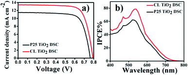 |
| | Fig. 11 (a) J–V characteristics DSCs of film using CL-like TiO2 and P-25, (b) the IPCE (%) of DSCs using P-25 and the CL TiO2. | |
Table 1 Thickness dependence PV parameters of the DSCs using the CF TiO2
| Thickness of the film (μm) |
Current density, Jsc (mA cm−2) |
Voc |
Fill factor (%) |
Efficiency (%) |
| 10 |
12.18 |
0.77 |
75.02 |
7.12 |
| 12 |
13.34 |
0.79 |
74.53 |
7.92 |
| 15 |
12.61 |
0.78 |
74.23 |
7.35 |
A comparison of the PV performance of the two materials indicated that Jsc and Voc were the two parameters that contributed to the enhancement of the efficiency for the leaf-like TiO2. High internal surface area of the material facilitates more dye adsorption on the photoanode film. This is evident from dye deloading data where intensity of dye de-loaded from CL TiO2 film was considerably higher than that from the P25 TiO2 film (Fig. 12a). Thus the increase in current density from 11.50 mA cm−2 to 13.44 mA cm−2 could be partly attributed to the increased dye loading. The other factor that contributes to the current density is the enhanced light scattering by the mesostructures. Each leaf-like structure of the CL TiO2 has the overall dimension of 1–2 μm that contributes to enhanced light scattering. A comparison of the reflectance spectra from CL TiO2 and P25 TiO2 photoelectrodes is given in Fig. 12b implying high light scattering property of the CL TiO2. According to the Mie theory, particles with sizes comparable to the wavelength of incident photons scatter light effectively. Light scattering increases the optical path of the light in the photoelectrode which will essentially increase the light interaction with dye molecules (light harvesting efficiency). The IPCE spectrum (Fig. 11b) showed substantial improvement at 650–750 nm wavelength regions (red part of the spectrum) compared to P-25 thus further revealing the contribution from the enhanced light scattering by the leaf-like TiO2 in the DSC.
 |
| | Fig. 12 (a) The UV-vis spectra of de-loaded dye from P-25 and CL TiO2 film in NaOH (b) reflectance spectrum showing enhanced light scattering property of CL TiO2 especially in the red part of the spectrum. | |
The recombination of photoexcited electrons in the conduction band of TiO2 with the I3− ions of the electrolyte is a major loss mechanism in DSCs which determines the overall power conversion efficiency of a DSC device.42 To have an idea about the effect of morphology on the electron transport, electrochemical impedance spectroscopy (EIS) was performed in both the P-25 and CL TiO2 DSCs. Parameters such as transport resistance (Rt), recombination resistance (Rct) and chemical capacitance (Cμ) in DSCs could be probed through EIS analysis. In the Nyquist plot, the semicircle around 101 Hz represents charge transfer at oxide–electrolyte interface.43 In Fig. 13a, the Nyquist plot shows higher impedance against recombination for the CL TiO2 DSC that is indicative of lower electron recombination with the I3− species in the electrolyte. The recombination resistance (the width of the semicircle at frequency range 101 Hz in Nyquist plot) needs to be larger to facilitate charge carriers accumulated in capacitive element to flow through external circuit. In the Bode phase plot (Fig. 13b), phase angle peak corresponds to the electron life time constant in the TiO2 film, from which electron life time was estimated using equation τn = 1/(2πf), where f is the frequency correspond to the phase angle peak. The value of f was shifted from 16.98 Hz (for P-25) to 3.80 Hz (for CL TiO2). Thus the respective electron lifetimes were found to be 9.37 ms and 41.86 ms, respectively in the two DSCs. The electrons live longer in the CL TiO2 DSC compared to that in the P-25 TiO2 film. In short we can attribute high surface area and light scattering property and better charge transport properties possessed by CL-shaped TiO2 for its superior PV performance over the P-25.
 |
| | Fig. 13 (a) Nyquist plot and (b) Bode phase plot of DSCs using CL TiO2 and P25 at dark. | |
Conclusions
Designing TiO2 nano/mesostructures with high surface area for dye loading and effective light scattering is a challenge in DSC research; however these are needed for high efficiency DSCs. In this present work we have designed leaf-like TiO2 mesostructures with high surface area and better light scattering capability through a modified titanate route from TiO2–SiO2 composite nanofibers. The initial and final materials were characterized by spectroscopy, microscopy and BET surface area measurements. DSCs employing the leaf-like TiO2 showed a power conversion efficiency of 7.92% which was ∼22% higher than that of commercial P-25 (6.5%).
Acknowledgements
Authors thank Ministry of New and Renewable Energy (MNRE), Govt. of India for financial support.
Notes and references
- B. O'Regan and M. Grätzel, Nature, 1991, 353, 737 CrossRef.
- M. Grätzel, Nature, 2001, 414, 338 CrossRef PubMed.
- A. Hagfeldt and M. Grätzel, Chem. Rev., 1995, 95, 49 CrossRef CAS.
- A. L. Linsebigler, G. Lu and J. T. Yates, Chem. Rev., 1995, 95, 735 CrossRef CAS.
- A. Mills and S. Le Hunte, J. Photochem. Photobiol., A, 1997, 108, 1 CrossRef CAS.
- P. Zhu, Y. Wu, M. V. Reddy, A. S. Nair, B. V. R. Chowdari and S. Ramakrishna, RSC Adv., 2012, 2, 531 RSC.
- J. Sundaramurthy, V. Aravindan, P. S. Kumar, S. Madhavi and S. Ramakrishna, J. Phys. Chem. C, 2014 DOI:10.1021/jp412787z.
- V. J. Babu, M. K. Kumar, A. S. Nair, T. L. Kheng, S. I. Allakhverdiev and S. Ramakrishna, Int. J. Hydrogen Energy, 2012, 37, 8897 CrossRef CAS PubMed.
- J. B. Veluru, K. K. Manippady, M. Rajendiren, K. M. Mya, P. R. Rayavarapu, S. N. Appukuttan and R. Seeram, Int. J. Hydrogen Energy, 2013, 38, 4324 CrossRef CAS PubMed.
- S. Berger, A. Ghicov, Y.-C. Nah and P. Schmuki, Langmuir, 2009, 25, 4841 CrossRef CAS PubMed.
- F. Campus, P. Bonhôte, M. Grätzel, S. Heinen and L. Walder, Sol. Energy Mater. Sol. Cells, 1999, 56, 281 CrossRef CAS.
- V. A. Ganesh, H. K. Raut, A. S. Nair and S. Ramakrishna, J. Mater. Chem., 2011, 21, 16304 RSC.
- V. A. Ganesh, S. S. Dinachali, A. S. Nair and S. Ramakrishna, ACS Appl. Mater. Interfaces, 2013, 5, 1527 CAS.
- D. L. Fedlheim and C. A. Foss, Metal Nanoparticles: Synthesis, Characterization and Applications, CRC Press, Boca Raton, 2002 Search PubMed.
- T. Sugimoto, Fine Particles: Synthesis, Characterization and Mechanisms of Growth, CRC Press, Boca Raton, 2000 Search PubMed.
- M. Grätzel, J. Sol-Gel Sci. Technol., 2001, 22, 7 CrossRef.
- C. M. Lieber and Z. L. Wang, MRS Bull., 2007, 32, 99 CrossRef CAS.
- K. D. Sattler, Handbook of Nanophysics: Nanotubes and Nanowires, CRC Press, Boca Raton, 2011 Search PubMed.
- S. Wang, Nanowires and Nanobelts: Materials Properties and Devices, Nanowires and Nanobelts of Functional Materials, Springer-Verlag, 2005 Search PubMed.
- G. K. Mor, K. Shankar, M. Paulose, O. K. Varghese and C. A. Grimes, Nano Lett., 2006, 6, 215 CrossRef CAS PubMed.
- R. Saito, G. Dresselhaus and M. Dresselhaus, Physical Properties of Carbon Nanotubes, Imperial College Press, London, 1999 Search PubMed.
- R. H. Baughman, A. A. Zakhidov and W. A. de Heer, Science, 2002, 297, 787 CrossRef CAS PubMed.
- Z. W. Pan, Z. R. Dai and Z. L. Wang, Science, 2001, 291, 1947 CrossRef CAS PubMed.
- Z. L. Wang, J. Nanosci. Nanotechnol., 2008, 8, 27 CrossRef CAS PubMed.
- Y. Qiu, W. Chen and S. Yang, Angew. Chem., Int. Ed., 2010, 49, 3675 CrossRef CAS PubMed.
- S. R. Gajjela, C. Yapa and P. Balaya, J. Mater. Chem., 2012, 22, 10873 RSC.
-
(a) Y. Zhou and M. Antonietti, J. Am. Chem. Soc., 2003, 125, 14960 CrossRef CAS PubMed;
(b) T. G. Deepak, G. S. Anjusree, T. Sara, T. A. Arun, S. V. Nair and A. S. Nair, RSC Adv., 2014, 4, 17615 RSC;
(c) Q. Zhang and G. Cao, Nano Today, 2011, 6, 91 CrossRef CAS PubMed;
(d) W.-Q. Wu, H.-S. Rao, Y.-F. Xu, Y.-F. Wang, C.-Y. Su and D.-B. Kuang, Sci. Rep., 2013, 3, 1892 Search PubMed.
- D. Li and Y. Xia, Nano Lett., 2003, 3, 555 CrossRef CAS.
- A. S. Nair, Z. Peining, V. J. Babu, Y. Shengyuan and S. Ramakrishna, Phys. Chem. Chem. Phys., 2011, 13, 21248 RSC.
- A. S. Nair, Y. Shengyuan, Z. Peining and S. Ramakrishna, Chem. Commun., 2010, 46, 7421 RSC.
- A. S. Nair, R. Jose, Y. Shengyuan and S. Ramakrishna, J. Colloid Interface Sci., 2011, 353, 39 CrossRef CAS PubMed.
- Y. Shengyuan, Z. Peining, A. S. Nair and S. Ramakrishna, J. Mater. Chem., 2011, 21, 6541 RSC.
- M. Y. Song, D. K. Kim, K. J. Ihn, S. M. Jo and D. Y. Kim, Nanotechnology, 2004, 15, 1861 CrossRef CAS.
- H. Kokubo, B. Ding, T. Naka, H. Tsuchihira and S. Shiratori, Nanotechnology, 2007, 18, 165604 CrossRef.
- T. Kasuga, M. Hiramatsu, A. Hoson, T. Sekino and K. Niihara, Adv. Mater., 1999, 11, 1307 CrossRef CAS.
- T. Kasuga, M. Hiramatsu, A. Hoson, T. Sekino and K. Niihara, Langmuir, 1998, 14, 3160 CrossRef CAS.
- T. A. Arun, D. K. Chacko, A. A. Madhavan, T. G. Deepak, G. S. Anjusree, T. Sara, S. Ramakrishna, S. V. Nair and A. S. Nair, RSC Adv., 2014, 4, 1421 RSC.
- A. S. Nair, P. Zhu, V. J. Babu, S. Yang, T. Krishnamoorthy, R. Murugan, S. Peng and S. Ramakrishna, Langmuir, 2012, 28, 6202 CrossRef CAS PubMed.
- E. Morgado, Jr., M. A. S. de Abreu, G. T. Moure, B. A. Marinkovic, P. M. Jardim and A. S. Araujo, Chem. Mater., 2007, 19, 665 CrossRef.
- A. S. Nair, Z. Peining, V. J. Babu, Y. Shengyuan, Y. Shengjie and S. Ramakrishna, RSC Adv., 2012, 2, 992 RSC.
- C. C. Tsai and H. Teng, Chem. Mater., 2006, 18, 367 CrossRef CAS.
- J. Bisquert, J. Phys. Chem. B, 2002, 106, 325 CrossRef CAS.
- K. Park, Q. Zhang, D. Myers and G. Cao, ACS Appl. Mater. Interfaces, 2013, 5, 1044 CAS.
|
| This journal is © The Royal Society of Chemistry 2014 |
Click here to see how this site uses Cookies. View our privacy policy here.