Controllable synthesis of ultrasmall CuInSe2 quantum dots for photovoltaic application

Chao-Feng Duab, Ting You*bc, Lei Jiangb, Song-Qiu Yangb, Kun Zoua, Ke-Li Hanb and Wei-Qiao Deng*b
aHubei Key Laboratory of Natural Products Research and Development, College of Chemistry and Life Sciences, China Three Gorges University, Yichang 443002, China
bState Key Laboratory of Molecular Reaction Dynamics, Dalian National Laboratory for Clean Energy, Dalian Institute of Chemical Physics, Chinese Academy of Sciences, Dalian 116023, China. E-mail: dengwq@dicp.ac.cn
cInternational Energy Research Center, Shanghai Jiaotong University, Shanghai 200030, China. E-mail: youting@sjtu.edu.cn

Received 20th May 2014 , Accepted 25th July 2014

First published on 30th July 2014


Abstract

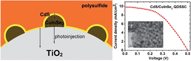
Here we report the first synthesis of ultrasmall CuInSe2 quantum dots (QDs) with diameters below the exciton Bohr radius 10.6 nm by a solvothermal method. The synthesis is conducted in oleylamine without any organometallic precursors. The quantum confinement effect has been identified in the optical absorption spectra. Through pre-loading CuInSe2 QDs on TiO2 film, a good electron transfer dynamics could be observed on the CdS/CuInSe2/TiO2 film. Under one sun of simulated irradiation, the resultant quantum dot sensitized solar cell based on CdS/CuInSe2 exhibited a power conversion efficiency of about 2.27%, which was 55% higher than that of the single CdS sensitized solar cell. It indicates that CuInSe2 QDs have great potential in photovoltaic applications.


1. Introduction

Quantum dots (QDs) with uniform sizes smaller than the bulk-material exciton Bohr radius have received considerable attention because of their unique properties afforded by the quantum confinement effect.1 These QDs confine electrons in a small box and quantise the energy band possessed by bulk materials into discrete energy states. QDs with quantum confinement structures produce remarkable changes in optical properties, leading various practical applications in biological imaging,2,3 lasing,4,5 photovoltaics,6,7 and light emitting diodes.8,9 Recently, II–VI-type10–12 (such as CdSe and CdS) and ternary chalcopyrite I–III–VI2-type13–15 (such as CuInS2, AgInS2) semiconductor QDs have been used as sensitizers for quantum dot-sensitized solar cells (QDSSCs). QDs display an electron–hole pair generation phenomenon with a quantum yield greater than 100%, called a “multiple exciton generation” or a “carrier multiplication”. These quantum dots are being used to develop solar cells that theoretically can exceed the Shockley–Queisser limit. The various ternary chalcopyrite I–III–VI2-type semiconductors are especially promising for QDSSC applications due to their high absorption coefficient and their direct band gap, which is well-matched to the solar spectrum. Notably, CuInSe2, which is representative of the I–III–VI2-type semiconductor, has attracted interest as a strong candidate for solar cells due to its small direct band gap of 1.04 eV and its large calculated exciton Bohr radius of 10.6 nm.16

CuInSe2 nanocrystals with sizes ranging from 20 to 100 nm have been synthesized extensively by several methods, including thermal decomposition,17 vapour–liquid–solid techniques,18 solid state reactions,19 solution–liquid–solid synthesis,20,21 organic solvent phase synthesis,12,22–25 and the solvothermal method.26–29 Castro et al.17 have reported that (PPh3)2CuIn(SePh)4 was used to synthesize CuInSe2 nanoparticles at 200–300 °C, which resulted in a largely aggregated chalcopyrite structure. Cui group18 successfully synthesized CuInSe2 nanowires with diameters ranging from 20–150 nm and lengths greater than 100 nm by vapour–liquid–solid techniques and solid-state reactions, respectively. Wang et al.22 reported the synthesis of chalcopyrite CuInSe2 nanocrystals with a size of 38 nm by the organic solvent phase synthesis method. Qian group26,27 has synthesized CuInSe2 nanoparticles with diameters of 80 nm via solvothermal reaction. However, compared to the successful synthesis of CuInSe2 nanocrystals with sizes larger than 20 nm, relatively few studies have reported the synthesis of CuInSe2 QDs with sizes smaller than 10 nm because it is difficult to control the size uniformity below the exciton Bohr radius.

Here we report the novel synthesis of CuInSe2 QDs with average diameters of 5 nm by a facile solvothermal method. Readily available CuCl, InCl3 and selenium reagents in an oleylamine (OLA) solvent were used to synthesize CuInSe2 QDs without any organometallic precursor or other toxic precursors, unlike traditional solvothermal methods. Furthermore, QDSSCs were fabricated using the as-synthesized CuInSe2 QDs as the co-sensitizer with CdS nanocrystals loaded on a multiporous TiO2 film. The fabricated CdS/CuInSe2 QDSSCs had a 2.27% power conversion efficiency under one-sun illumination (AM1.5G, 100 mW cm−2), which was 55% higher than that of CdS QDSSCs.

2. Experimental details

2.1 Materials

All reagents were of analytical grade and used without any further purification, otherwise noted specifically. Oleylamine (OLA, 80–90%, Acros), Selenium powder (99%, Tianjin Chemical Reagent Co., Ltd), InCl3·4H2O (99.99%-In, Acros), CuCl (Tianjin Chemical Reagent Co., Ltd), 2-mercaptopropionic acid (MPA, 95%, Aldrich), tetramethylammonium hydroxide solution (25 wt% in methanol, Aldrich), hexane, ethanol, methanol and ethyl acetate were of analytical grade and obtained commercially.

2.2 Synthesis of CuInSe2 QDs

The oleylamine solutions of copper/indium and selenium were each prepared as reported in the literatures.30,31 CuCl (0.01 mmol) and InCl3·4H2O (0.01 mmol) were mixed with oleylamine (0.99 mL) at room temperature, and the mixture was heated to 120 °C under an Ar atmosphere. This heating was maintained for 1 h with vigorous magnetic stirring until a clear solution was formed. Then, 1 mL of oleylamine and 0.5 mmol of Se powder were deposited into a separate flask, heated to 120 °C for 0.5 h under vacuum, and placed under an Ar atmosphere for the remainder of the synthetic reaction. The solution was then heated to 250 °C and maintained at that temperature for 10 min. Over the course of an hour, the solution gradually changed from colourless to orange and then to brownish red because of the dissolution of the Se powder in the oleylamine. The copper/indium and selenium solutions were then mixed in a Teflon-lined stainless steel autoclave (25 mL) containing 15 mL of hexane under vigorous stirring at a constant temperature of 170 °C for 2 h. After the autoclave was cooled to room temperature, the product was precipitated with an ethanol–methanol (1–2, v/v) solution. The OLA-capped QDs were then obtained by centrifuging at 6790 rcf ( × g) for 10 min. For comparison, parallel experiments were also conducted at different solvothermal temperatures.

For the application of CuInSe2 QDs in QDSSCs, the as-synthesized quantum dots were surface modified because it has been reported that MPA-capped QDs load more efficiently onto the TiO2 film.32 To synthesize the MPA-capped CuInSe2 QDs, dried OA-capped CuInSe2 QDs were first dispersed in a methanol solution containing 60 mM MPA and 70 mM tetramethylammonium hydroxide. Then, the mixture was ultrasonicated for 30 min. The MPA-capped CuInSe2 QDs were precipitated with an ethyl acetate–hexane solution and then redispersed in methanol.31,33

2.3 Fabrication of quantum dot-sensitized solar cells

A screen-printed TiO2 film (6 μm in thickness) was used as the photoanode. A TiO2 paste consisting 1.0 g of P25 powder, 0.5 g of ethyl cellulose, 0.4 g of terpinol in ethanol was printed on a fluorine-doped SnO2 (FTO, 14 Ω square−1, 2.2 mm thickness, NSG Group, Tokyo, Japan) conducting glass electrode, which was used as the transparent layer. Then, a 4 μm-thick light-scattering layer was spread on the top of the transparent layer and subsequently sintered at 500 °C in flowing compressed air for 1 h. The TiO2 film was then dipped into the methanol solution containing the MPA-capped CuInSe2 QDs for 24 h, resulting in the formation of a CuInSe2-sensitized photoanode. For the CdS/CuInSe2-sensitized photoanodes, the film needed to be dipped into a 0.05 M Cd(NO3)2 ethanol solution for 30 s, rinsed with ethanol, and then dipped for another 30 s into a 0.05 M Na2S methanol solution and rinsed with methanol. This two-step dipping procedure was considered to be a single SILAR cycle, and this SILAR cycle was repeated 11 times. A CdS-only-sensitized photoanode was also prepared using the SILAR process.

The cells were prepared by sealing the QD-sensitized FTO/TiO2 electrode and a Cu2S-coated counter electrode34 using a 50 μm-thick Bynel (DuPont) hot-melt gasket. The active area of the cell was 0.16 cm2. A solution of 1 M sodium sulfide and 1 M sulfur dissolved in water was used as the liquid electrolyte.

2.4 Characterization

The X-ray powder diffraction (XRD) patterns were recorded using a Rigaku D/max-2500/PC diffractometer with Cu Kα radiation (λ = 0.15406 nm). High-resolution transmission electron microscopy (HRTEM) images were obtained using a FEI Tecnai G2 F30 S-Twin transmission electron microscope. The absorption spectra were recorded using a Jasco V550 UV-Vis spectrometer on quartz plate (1 mm in thickness) with CuInSe2 QDs, CdS and CdS/CuInSe2 QDs sensitized TiO2 mesoporous thin film (2 μm in thickness).

2.5 Measurement

The current density–voltage (IV) characteristics were measured with a Keithley 2400 Sourcemeter, and the cell was subjected to the irradiation of a solar simulator (Abet-technologies, USA, SUN2000) operating at one sun illumination (AM1.5, 100 mW cm−2). The incident photon to current conversion efficiency (IPCE) was measured with a QE/IPCE Measurement Kit (Oriel, USA, M66901) in the wavelength range of 400–900 nm. Time resolved transient absorption spectra were recorded using a transient absorption (TA) spectrometer with femtosecond resolution.35 The laser used for excitation was a Hurricane Ti:Sapphire laser system (Spectra Physics) capable of 800 nm laser pulses of 1 mJ pulse−1 (width of 130 fs) at a rate of 1 kHz. A fraction (5%) of the beam was used to generate a probe pulse. The second harmonic (400 nm, 500 nJ pulse−1) was used for excitation of the sample.

3. Results and discussion

Fig. 1(a) shows the powder X-ray diffraction (XRD) pattern of the as-synthesized CuInSe2 QDs. The diffraction peaks were indexed to the tetragonal chalcopyrite structure of CuInSe2 (JCPDS no. 40-1487); however, the observed diffraction peaks were broadened due to the small crystal size. Using the Debye-Scherrer formula, the average crystal size was determined to be 5 nm. The TEM image of CuInSe2 QDs, shown in Fig. 1(b), reveals that these QDs have an average diameter of 5 nm, which is close to the size calculated from the XRD measurement. The inset in Fig. 1(b) is the HRTEM image of a single quantum dot displaying a visible lattice fringe, indicating that the as-synthesized CuInSe2 QDs are highly crystalline. The observed lattice spacing was calculated to be ∼0.32 nm, corresponding to that of the (112) planes of CuInSe2.
image file: c4ra04727c-f1.tif
Fig. 1 (a) XRD pattern and (b) TEM images of the CuInSe2 QDs grown at 170 °C for 2 h. The inset to (b) shows the HRTEM image of a single quantum dot.

The UV-Vis absorbance spectrum of the colloidal CuInSe2 QDs was measured to probe their optical band gaps. This result shows an absorption peak centered at approximately 440 nm (Fig. 2). The band gap of the CuInSe2 QDs was determined from the fundamental absorption edge of the spectrum,36 which is shown in the inset of Fig. 2. Using the direct band gap method,12 the band gap of the CuInSe2 QDs was calculated to be 2.24 eV. The distinct blue shift of the absorption wavelength of the as-synthesized CuInSe2 QDs relative to that of bulk CuInSe2 indicates that the size of the CuInSe2 QDs is undoubtedly in the quantum confinement region.


image file: c4ra04727c-f2.tif
Fig. 2 The typical absorption spectrum of the CuInSe2 QDs dispersed in toluene. The squared absorption coefficient plotted as a function of energy (inset) displays a linear trend for a direct transition.

The as-synthesized CuInSe2 QDs, the CdS QDs and combination of them were loaded onto the TiO2 electrodes, respectively. Fig. 3 shows the UV-Vis absorption spectra of the CuInSe2/TiO2, CdS/TiO2 and CdS/CuInSe2/TiO2 photoanodes. The absorption onset occurred at ∼550 nm for the CuInSe2 photoanode and at ∼600 nm for the CdS photoanode. The co-sensitization effect of CdS/CuInSe2 was clearly observed by the extension of the absorption range and the increase in the absorbance. The enhancement absorption of the CdS/CuInSe2 photoanode shifted to the long wavelength region due to the remission of the quantum confinement effect on the CuInSe2 QDs.


image file: c4ra04727c-f3.tif
Fig. 3 UV-Vis absorption spectra of TiO2 films sensitized with CuInSe2, CdS and CdS/CuInSe2 QDs.

To assess the photovoltaic application of the CuInSe2 QDs, QDSSCs with different sensitizers were fabricated in typical sandwich geometry, consisting of QDs sensitized with TiO2 electrodes, a polysulfide electrolyte, and a Cu2S-coated counter electrode. Fig. 4(a) shows the photocurrent–voltage (IV) characteristics of the QDSSCs that were produced using CuInSe2, CdS, and CdS/CuInSe2 QDs as sensitizers, named as CdS, CuInSe2, and CdS/CuInSe2 QDSSC, respectively. The open circuit potential (VOC), short circuit current density (JSC), fill factor (FF), and total energy conversion efficiency (η) of these cells are listed in Table 1. The efficiencies measured for CuInSe2 and CdS QDSSCs were 0.10% and 1.46%, respectively. For the CdS/CuInSe2 QDSSC, VOC and FF decreased compared with CdS QDSSC, and JSC increased markedly to 9.82 mA cm−2. The efficiency obtained for a CdS/CuInSe2 QDSSC was 2.27%, which was 55% greater than that of a CdS QDSSC. Additionally, the photocurrent of the CdS/CuInSe2 QDSSC was greater than the sum of the photocurrents of single CuInSe2 and CdS QDSSCs. This result indicates that the photocurrent of the CdS/CuInSe2 electrode increases significantly with the pre-loaded CuInSe2 QDs, which is advantageous to the electron injection and the hole recovery of CdS electrodes. To investigate the combination-sensitization effect of CuInSe2 and CdS QDs on the cascade structures, the incident photon to current conversion efficiencies (IPCE) were measured from the JSC monitored at different excitation wavelengths. The IPCE measurements are shown in Fig. 4(b). These results coincide with the efficiencies shown in Fig. 4(a). As these results reveal, IPCE values as high as 75% can be achieved by the CdS/CuInSe2 QDSSC, but the value obtained by the CdS QDSSC was only ∼50%. The IPCE results indicate that excited electrons in CdS/CuInSe2 QDSSC can be injected into TiO2 and collected by the electrode more efficiently than the CdS QDSSC. Overall, these findings indicate that CuInSe2 QDs could efficiently improve the performance of CdS QDSSC with cascade structures. A previous literature reported the introduction of ZnS into CdS/CdSe cosensitized solar cell can boost the cell efficiency up to 4.22%,12 we expect similar approach may enhance the cell efficiency further.


image file: c4ra04727c-f4.tif
Fig. 4 (a) IV characteristics and (b) IPCE spectra of QDSSCs measured under 100 mW cm−2 of simulated AM 1.5G irradiation.
Table 1 Results obtained from the photocurrent–voltage (IV) measurements of the QDSSCs using various electrodes
QDSSC VOC (V) JSC (mA cm−2) FF η (%)
CuInSe2 0.201 1.10 45.9 0.10
CdS 0.439 6.85 48.4 1.46
CdS/CuInSe2 0.497 9.82 46.6 2.27


Time-resolved transient absorption spectroscopy is a convenient way to probe the charge separation and charge transfer processes in quantum dots as well as confirm the existence of species that exist primarily on the picosecond time scale. In the present study we deposited CdS on quartz slide, on TiO2 and CuInSe2 sensitized TiO2 (CuInSe2/TiO2) film to measure the pump-probe transient absorption spectroscopy. Fig. 5(a)–(c) show the time-resolved transient absorption spectra recorded at different times following 400 nm laser excitation of CdS/SiO2, CdS/TiO2, and CdS/CuInSe2/TiO2. When excited at 400 nm, the CdS/SiO2, CdS/TiO2 and CdS/CuInSe2/TiO2 films showed a bleaching in the 460–510 nm region. As the previous studies reported that with increasing decay time the bleaching recovers as the separated charges disappear either via recombination or by electron transfer to TiO2.37 The transient bleaching, which represents charge separation within the CdS nanocrystals, recovers over a period of several nanoseconds to occur at a faster rate. Quick removal of one of the charge carriers by an acceptor species causes the bleaching recovery.38 Fig. 5(d) compares the bleaching recovery recorded following 400 nm laser pulse excitation of CdS/SiO2, CdS/TiO2 and CdS/CuInSe2/TiO2 at the corresponding bleaching maximum. On TiO2 (bare TiO2 and CuInSe2-sensitized TiO2) films, the recovery become faster as the electrons are transferred across CdS/TiO2 (CdS/CuInSe2/TiO2) interface. These recovery traces exhibit multiexponential behavior and can be fitted to biexponential kinetics convoluted with the instrument response function using eqn (1) with fitted values in Table S1(ESI).

 
image file: c4ra04727c-t1.tif(1)


image file: c4ra04727c-f5.tif
Fig. 5 Time-resolved transient absorption spectra recorded following 400 nm laser pulse excitation of CdS quantum dots deposited on (a) SiO2 slice, (b) TiO2 and (c) CuInSe2 pre-sensitized TiO2 porous film. (d) The bleaching recovery normalized to peak response. The monitoring wavelengths are at the bleaching maximum.

In the present experiments, on CdS/SiO2 slice, it exhibits the lowest bleaching recovery (τ1 = 17.9 ps and τ2 = 194.8 ps) due to the excited electrons disappear via recombination but not transfer, because SiO2 is electronically insulating and will not participate in the interparticle electron transfer process. While the bleaching recovers faster in the CdS/CuInSe2/TiO2 sample (τ1 = 7.0 ps and τ2 = 80.8 ps) than CdS/TiO2 (τ1 = 9.1 ps and τ2 = 117.8 ps), arises as the electron transfer to CuInSe2/TiO2 dominates the deactivation of excited CdS. For comparison purposes, an average lifetime has been determined using eqn (2).39

 
image file: c4ra04727c-t2.tif(2)

For CdS alone, it exhibits a relatively long-lived bleaching recovery with average lifetime of 183 ps. A decrease in the average CdS bleaching recovery lifetime was evident when deposited on TiO2 film and a dramatic decrease on CuInSe2/TiO2 film with average lifetimes of 107 and 70 ps, respectively. If we assumed that electron transfer is the dominant pathway responsible for the faster bleaching recovery of CdS on TiO2 (bare TiO2 and CuInSe2 sensitized TiO2) surface, we can estimate the electron transfer rate using the eqn (3).

 
image file: c4ra04727c-t3.tif(3)

The electron transfer rates for CdS/TiO2 and CdS/CuInSe2/TiO2 are 2.97 × 10⁹ and 7.92 × 10⁹ s−1, respectively. Based on these results, it can be observed that an increase in the electron transfer rate constant caused by sensitized CuInSe2 QDs on TiO2 film. This means that more efficient electron injection dynamics in CdS/CuInSe2/TiO2 film, which consisted with the better performance of CdS/CuInSe2 QDSSC.

The schematic illustration of the cascade structural photoelectrode and the corresponding energy diagram are shown in Fig. 6 to elucidate the probable charge transfer mechanisms involved in the irradiated electrodes. The band gaps of TiO2 and CdS are ∼3.2 eV and 2.4 eV (conduction band edge to the vacuum are approximately 4.0 and 3.6 eV), respectively.40 Based on the analysis of Fig. 2, the band gap of the as-synthesized CuInSe2 QDs is ∼2.2 eV. It was reported that the CuInSe2 conduction band edge is 0.2 eV above the CdS conduction band edge.41 As shown in Fig. 6(b), under white light illumination, the combined sensitizers are both exited. For CuInSe2 QDs, the photogenerated electrons transfer from their conduction band to TiO2. For CdS, similar to that of CuInSe2, photogenerated electrons transfer into TiO2 where CdS are attached to TiO2 directly (Fig. 6, dash line). However, where CdS are contacted with CuInSe2 QDs, the interconduction band transfer of electrons from CdS to CuInSe2 QDs is prohibited because the edge of the conduction band of the CuInSe2 QDs is higher than that of the CdS. As the literature reported, the electrons in the conduction band of the CdS would scavenge the holes in the CuInSe2 QDs, which can substantially enhance the separation of photogenerated charges in the CuInSe2 QDs and thus enhance the photocurrent of the electrode.15


image file: c4ra04727c-f6.tif
Fig. 6 (a) Schematic illustration and (b) the corresponding energy level schematic diagram of the photoelectrode consisting of a TiO2 film sensitized with CuInSe2 QDs and CdS.

We also synthesized CuInSe2 QDs at different solvothermal temperatures. As shown in Fig. S1, the QDs synthesized at different temperatures showed different colors. The TEM image in Fig. S2 showed that the average sizes of QDs synthesized at 190 °C are 20 nm. Because of quantum confinement effect, the QDs with large sizes show darker colors. The as-synthesized quantum dots were used as sensitizers for the QDSSCs. The IV characteristics of these QDSSCs are shown in Fig. S3 and Table S2 (ESI). The efficiencies measured for a CdS/CuInSe2(150 °C) QDSSC and a CdS/CuInSe2(190 °C) QDSSC were 1.63% and 1.10%, respectively (shown in Table S2 ESI). The different efficiencies of these solar cells should be caused by the quantum dots synthesized at different temperatures. In the case of low solvothermal temperature at 150 °C, it was possible that Ostwald ripening did not affect crystal growth, and the uniform QDs with small sizes were obtained. However, due to the short reaction time, the crystal structures of the QDs (150 °C) were not intact compared to that of QDs (170 °C). Thus the corresponding the CdS/CuInSe2 (150 °C) QDSSC exhibited lower photocurrent value and efficiency than the CdS/CuInSe2 (170 °C) QDSSC. Contrastingly, when the solvothermal temperature increased to 190 °C, the reaction proceeded fast and Ostwald ripening started to increase the sizes of quantum dots. Therefore, the CuInSe2 QDs obtained at 190 °C were larger than that of 170 °C, implying that steric hindrance may hinder the binding of QDs (190 °C) to the TiO2 film. The photocurrent and voltage of CdS/CuInSe2 (190 °C) QDSSCs were both lower than those of CdS/CuInSe2 (170 °C) QDSSCs, which resulted in poor efficiencies.

4. Conclusions

In summary, ultrasmall CuInSe2 quantum dots below 5 nm have been successfully synthesized by a facile solvothermal method. The CuInSe2 QDs were used as a combination-sensitizer for the cascade structure of the CdS/CuInSe2 QDSSCs to improve their performances. Under one sun of simulated irradiation (AM1.5G, 100 mW cm−2), the cell efficiency reached a promising 2.27%, which was 55% higher than that of the single CdS sensitized solar cell. A good electron transfer dynamics could be observed on CdS/CuInSe2/TiO2 film. The preliminary CuInSe2 layer is not only energetically favorable to electron transfer but behaves as a hole scavenger for excited CdS.

Acknowledgements

This work was supported by NSFC 91333116, NSFC 21373202, NSFC 21173209, “talent 100” program of Chinese Academy of Sciences and “Chutian” project of China Three Gorges University.

References

  1. L. Brus, App. Phys. A: Mater. Sci. Process., 1991, 53, 465–474 CrossRef.
  2. M. Bruchez, M. Moronne, P. Gin, S. Weiss and A. P. Alivisatos, Science, 1998, 281, 2013–2016 CrossRef CAS.
  3. A. P. Alivisatos, W. Gu and C. Larabell, Annu. Rev. Biomed. Eng., 2005, 7, 55–76 CrossRef CAS PubMed.
  4. M. Kazes, D. Y. Lewis, Y. Ebenstein, T. Mokari and U. Banin, Adv. Mater., 2002, 14, 317 CrossRef CAS.
  5. E. Plum, V. Fedotov, P. Kuo, D. Tsai and N. Zheludev, Opt. Express, 2009, 17, 8548–8551 CrossRef CAS.
  6. A. Nozik, M. Beard, J. Luther, M. Law, R. Ellingson and J. Johnson, Chem. Rev., 2010, 110, 6873–6890 CrossRef CAS PubMed.
  7. W. Ma, S. L. Swisher, T. Ewers, J. Engel, V. E. Ferry, H. A. Atwater and A. P. Alivisatos, ACS Nano, 2011, 5, 8140–8147 CrossRef CAS PubMed.
  8. K. Bae, J. Kwak, J. W. Park, K. Char, C. Lee and S. Lee, Adv. Mater., 2009, 21, 1690–1694 CrossRef PubMed.
  9. J. Caruge, J. Halpert, V. B. Wood and M. Bawendi, Nat. Photonics, 2008, 2, 247–250 CrossRef CAS.
  10. J. Chen, J. L. Song, X. W. Sun, W. Q. Deng, C. Y. Jiang, W. Lei, J. H. Huang and R. S. Liu, Appl. Phys. Lett., 2009, 94, 153115 CrossRef PubMed.
  11. L. Li, X. C. Yang, J. J. Gao, H. N. Tian, J. Z. Zhao, A. Hagfeldt and L. C. Sun, J. Am. Chem. Soc., 2011, 133, 8458–8460 CrossRef CAS PubMed.
  12. Y. L. Lee and Y. S. Lo, Adv. Funct. Mater., 2009, 19, 604–609 CrossRef PubMed.
  13. Q. Guo, S. J. Kim, M. Kar, W. N. Shafarman, R. W. Birkmire, E. A. Stach, R. Agrawal and H. W. Hillhouse, Nano Lett., 2008, 8, 2982–2987 CrossRef CAS PubMed.
  14. T. L. Li, Y. L. Lee and H. Teng, Energy Environ. Sci., 2012, 5, 5315–5324 CAS.
  15. T. L. Li, Y. L. Lee and H. Teng, J. Mater. Chem., 2011, 21, 5089–5098 RSC.
  16. H. Zhong, Z. Wang, E. Bovero, Z. Lu, F. C. J. M. van Veggel and G. D. Scholes, J. Phys. Chem. C, 2011, 115, 12396–12402 CAS.
  17. S. L. Castro, S. G. Bailey, R. P. Raffaelle, K. K. Banger and A. F. Hepp, Chem. Mater., 2003, 15, 3142–3147 CrossRef CAS.
  18. H. Peng, D. T. Schoen, S. Meister, X. F. Zhang and Y. Cui, J. Am. Chem. Soc., 2007, 129, 34–35 CrossRef CAS PubMed.
  19. D. T. Schoen, H. Peng and Y. Cui, J. Am. Chem. Soc., 2009, 131, 7973–7975 CrossRef CAS PubMed.
  20. C. Steinhagen, V. A. Akhavan, B. W. Goodfellow, M. G. Panthani, J. T. Harris, V. C. Holmberg and B. A. Korgel, ACS Appl. Mater. Interfaces, 2011, 3, 1781–1785 CAS.
  21. A. J. Wooten, D. J. Werder, D. J. Williams, J. L. Casson and J. A. Hollingsworth, J. Am. Chem. Soc., 2009, 131, 16177–16188 CrossRef CAS PubMed.
  22. W. Wang, Z. Jin and H. Liu, J. Am. Ceram. Soc., 2011, 94, 2571–2577 CrossRef CAS PubMed.
  23. J. Y. Chang, M. H. Tsai, K. L. Ou, C. H. Yang and J. C. Fan, CrystEngComm, 2011, 13, 4236–4243 RSC.
  24. M. Kar, R. Agrawal and H. W. Hillhouse, J. Am. Chem. Soc., 2011, 133, 17239–17247 CrossRef CAS PubMed.
  25. B. Koo, R. N. Patel and B. A. Korgel, J. Am. Chem. Soc., 2009, 131, 3134–3135 CrossRef CAS PubMed.
  26. B. Li, Y. Xie, J. Huang and Y. Qian, Adv. Mater., 1999, 11, 1456–1459 CrossRef CAS.
  27. Y. Jiang, Y. Wu, X. Mo, W. Yu, Y. Xie and Y. Qian, Inorg. Chem., 2000, 39, 2964–2965 CrossRef CAS.
  28. C. C. Wu, C. Y. Shiau, D. W. Ayele, W. N. Su, M. Y. Cheng, C. Y. Chiu and B. J. Hwang, Chem. Mater., 2010, 22, 4185–4190 CrossRef CAS.
  29. H. Chen, S.-M. Yu, D.-W. Shin and J.-B. Yoo, Nanoscale Res. Lett., 2010, 5, 217–223 CrossRef CAS PubMed.
  30. J. Tang, S. Hinds, S. O. Kelley and E. H. Sargent, Chem. Mater., 2008, 20, 6906–6910 CrossRef CAS.
  31. T. L. Li and H. Teng, J. Mater. Chem., 2010, 20, 3656–3664 RSC.
  32. J. Chen, D. Zhao, J. Song, X. Sun, W. Deng, X. Liu and W. Lei, Electrochem. Commun., 2009, 11, 2265–2267 CrossRef CAS PubMed.
  33. K. S. Leschkies, R. Divakar, J. Basu, E. Enache-Pommer, J. E. Boercker, C. B. Carter, U. R. Kortshagen, D. J. Norris and E. S. Aydil, Nano Lett., 2007, 7, 1793–1798 CrossRef CAS PubMed.
  34. Z. Chen, W. Peng, K. Zhang, J. Zhang, M. Yanagida and L. Han, Nanoscale, 2012, 4, 7690–7697 RSC.
  35. S. Yang, J. Liu, P. Zhou, K. Han and G. He, Chem. Phys. Lett., 2011, 512, 66–69 CrossRef CAS PubMed.
  36. C. Joseph and C. Menon, J. Phys. D: Appl. Phys., 2001, 34, 1143 CrossRef CAS.
  37. D. R. Baker and P. V. Kamat, J. Phys. Chem. C, 2009, 113, 17967–17972 CAS.
  38. B. Farrow and P. V. Kamat, J. Am. Chem. Soc., 2009, 131, 11124–11131 CrossRef CAS PubMed.
  39. D. R. James, Y.-S. Liu, P. De Mayo and W. R. Ware, Chem. Phys. Lett., 1985, 120, 460–465 CrossRef CAS.
  40. R. Vogel, P. Hoyer and H. Weller, J. Phys. Chem., 1994, 98, 3183–3188 CrossRef CAS.
  41. M. Turowski, M. Kelly, G. Margaritondo and R. Tomlinson, Appl. Phys. Lett., 1984, 44, 768–770 CrossRef CAS PubMed.

Footnote

Electronic supplementary information (ESI) available. See DOI: 10.1039/c4ra04727c

This journal is © The Royal Society of Chemistry 2014
Click here to see how this site uses Cookies. View our privacy policy here.