
BiFeO3 thin films prepared on metallic Ni tapes by chemical solution deposition: effects of annealing temperature and a La0.5Sr0.5TiO3 buffer layer on the dielectric, ferroelectric and leakage properties
Xianwu Tanga,
Ling Hua,
Jie Yanga,
Li Chena,
Jianming Daia,
Wenhai Songa,
Zhaorong Yanga,
Xuebin Zhu*a and
Yuping Sun*ab
aKey Laboratory of Materials Physics, Institute of Solid State Physics, Chinese Academy of Sciences, Hefei 230031, China. E-mail: xbzhu@issp.ac.cn
bHigh Magnetic Field Laboratory, Chinese Academy of Sciences, Hefei 230031, China. E-mail: ypsun@issp.ac.cn
First published on 14th July 2014
Abstract
In this work, BiFeO3 (BFO) thin films were prepared on metallic Ni (200) tapes with and without a La0.5Sr0.5TiO3 (LSTO) buffer layer at different temperatures by chemical solution deposition. The effects of the annealing temperature as well as the LSTO buffer layer on the dielectric, leakage and ferroelectric properties have been studied in detail. The crystallite size, dielectric constant and leakage current density increase, while the coercive field decreases with increasing annealing temperature. The BFO thin films deposited directly on the Ni tapes are prone to wrinkling, while the wrinkles are smoothed by introducing a thin LSTO buffer layer. Decreased compressive microstrain as well as improved ferroelectric and leakage properties are observed in the BFO thin films deposited on the LSTO buffered Ni tapes. The results will provide an instructive route to optimize BiFeO3-based thin films on metallic tapes by chemical solution deposition methods.
1 Introduction
BiFeO3 (BFO) thin films, over the last decade, have drawn significant interest and been widely investigated due to their ferroelectric and magnetic properties at room temperature. BFO has a ferroelectric order with a Curie temperature of 850 °C.1 On the one hand, BFO thin films have complementary ferroelectric polarizations as compared to the traditional ferroelectric lead zirconate titanate and barium titanate thin films. These make BFO interesting for use in ferroelectric random access memories, optical modulators, waveguides, and microelectromagnetic systems.2 On the other hand, the lead-free characteristics of BFO are promising for environmentally friendly devices. However, to date, most BFO thin films have been deposited on single-crystal substrates3,4 and platinized silicon wafers.5–7 From an application point of view, such substrates are expensive, rigid, and worthless in very limited sizes. Replacing these substrates with metallic tapes such as Ni, Cu, Al, and Fe is attractive commercially, due to their low cost and simple patterning methods.8 Additionally, among these base metals, Ni tape possesses lower resistivity, flexibility and other alluring functionalities.9 Technologically, the integration of Ni tapes as inner electrodes and substrates within capacitors to form multilayer capacitors will be very important for device applications.10 However, there are some problems with integrating an oxide ferroelectric thin film onto the metal tapes.11,12 One problem is the possibility of substrate oxidation, which will decrease the conductivity of the electrode. The other is the creation of a nonferroelectric interfacial layer caused by the interfacial reaction, and interdiffusion between the substrate and the thin film, which will degrade the properties and the performance. Additionally, wrinkles resulting from the large mismatches in the thermal expansion coefficient and lattice constant between the ferroelectric thin film and the metal tapes will also downgrade the properties.9 Nevertheless, these problems can be resolved by the introduction of a buffer layer. As previously reported,13 a buffer layer is necessary to suppress the diffusion of metal atoms from the substrate to the thin film as well as oxygen atoms from the thin film to the metal tape, and the wrinkles will also be smoothed by the introduction of a buffer layer.Recently, it has been reported that the desired ferroelectric, piezoelectric, and magnetoelectric properties can be obtained in pulsed laser deposition (PLD)-derived BFO thin films deposited directly on Ni14 and NiW15 tapes. However, even though very high quality films can be made by PLD, the method is not very suitable for industrialization due to its high cost and limited scale. To date, various methods have been used to prepare BFO thin films and to optimize their properties.6,7,16–22 Among these methods, chemical solution deposition (CSD) is widely used due to its low cost, precise control of the stoichiometry, ability to achieve atomic-scale mixing, and easy processing of large-area thin films.23
In this article, BFO thin films have been prepared on metallic Ni tapes by CSD. The effects of the annealing temperature as well as the introduction of a La0.5Sr0.5TiO3 (LSTO) buffer layer have been investigated systematically. The results will provide an instructive route to optimize BFO-based thin films metallic tapes by chemical solution deposition.
2 Experimental
Both the LSTO and BFO thin films were fabricated on flexible Ni (200) tape via CSD methods. The LSTO buffered layers were deposited on the Ni tapes as in our previous report.24 La-acetate, Sr-acetate, Ti-n-butoxide, and propionic acid were used as raw materials for preparing the LSTO precursor solution with a concentration of 0.1 M. Then, the thin films were prepared using a spin coater with a rotation speed of 4000 rpm for 30 s, pyrolyzed at 300 °C for 10 minutes in air, and then annealed at 900 °C in a forming gas (4% H2 and 96% N2) for 1 h. In order to enhance the thin film thickness, the spin coating, pyrolysis and annealing processes were repeated twice, which gave the thin film a thickness of about 20 nm.BFO thin films were prepared by the CSD method as in our previous reports.6,7 A 3 mol% excess amount of bismuth nitrate pentahydrate was used to compensate the bismuth loss during processing. BFO thin films were deposited on Ni (200) tapes with and without a LSTO buffer layer by spin coating. The thin films were annealed at different temperatures (475, 500, 525, and 550 °C) for 30 minutes in a nitrogen atmosphere. Here, the BFO/Ni thin films annealed at 475, 500, 525, and 550 °C are denoted as N475, N500, N525 and N550 respectively, and the BFO/LSTO/Ni thin films annealed at 475, 500, 525, and 550 °C are denoted as NL475, NL500, NL525 and NL550 respectively.
The crystallization quality was checked using X-ray diffraction (XRD) performed with a Philips X'pert Pro diffractometer with Cu Kα radiation. Field-emission scanning electron microscopy (FE-SEM, FEI Sirion 200 type, FEI, Hillsboro, OR) was used to analyse both the thin film thickness and surface morphology, and all the thin films have a thickness of about 488 nm. Top Au electrodes 0.2 mm in diameter were deposited by sputtering, using small ion sputtering equipment (SBC-12, KYKY, Beijing), onto the surface of BFO through a shadow mask. The dielectric response was investigated within the frequency range of 0–1 MHz with a driving voltage of 0.1 V by a precision inductance, capacitance, and resistance (LCR) meter (TH2828/A/S, Tonghui Electronic Co., LTD, Changzhou). The ferroelectric and leakage properties, as well as the pulsed polarization positive up negative down (PUND) measurements at a pulse width of 0.05 ms and a delay time of 1 s, were investigated using a Sawyer-Tower circuit attached to a computer-controlled standardized ferroelectric test system (Radiant Precision Premier II, Radiant Technologies, USA).
3 Results and discussion
3.1 Microstructure
Fig. 1(a) and (b) show the XRD patterns of the BFO/Ni and BFO/LSTO/Ni thin films, respectively. All the obtained BFO thin films are randomly oriented without parasitic phases. Each diffraction peak of the BFO thin films can be indexed to a perovskite structure with a pseudocubic unit cell. The averaged crystallite size is calculated using the three most intense peaks, namely the (001), (110) and (![[1 with combining macron]](https://www.rsc.org/images/entities/char_0031_0304.gif) 10) peaks, by the Scherrer equation. The variation of the derived crystallite size with the annealing temperature for the BFO/Ni and BFO/LSTO/Ni thin films is shown in the corresponding insets of Fig. 1(a) and (b). It is observed that the crystallite size increases linearly with increasing annealing temperature, no matter whether a LSTO buffer layer is used, which is the same as in the previous report.7 Moreover, the BFO/LSTO/Ni thin films show crystallite size similar to that of the BFO/Ni for each given annealing temperature. Both the results of the random orientation and the same crystallite size suggest that the LSTO buffer layer does not influence nucleation in the bulk of the BFO thin films.
10) peaks, by the Scherrer equation. The variation of the derived crystallite size with the annealing temperature for the BFO/Ni and BFO/LSTO/Ni thin films is shown in the corresponding insets of Fig. 1(a) and (b). It is observed that the crystallite size increases linearly with increasing annealing temperature, no matter whether a LSTO buffer layer is used, which is the same as in the previous report.7 Moreover, the BFO/LSTO/Ni thin films show crystallite size similar to that of the BFO/Ni for each given annealing temperature. Both the results of the random orientation and the same crystallite size suggest that the LSTO buffer layer does not influence nucleation in the bulk of the BFO thin films.
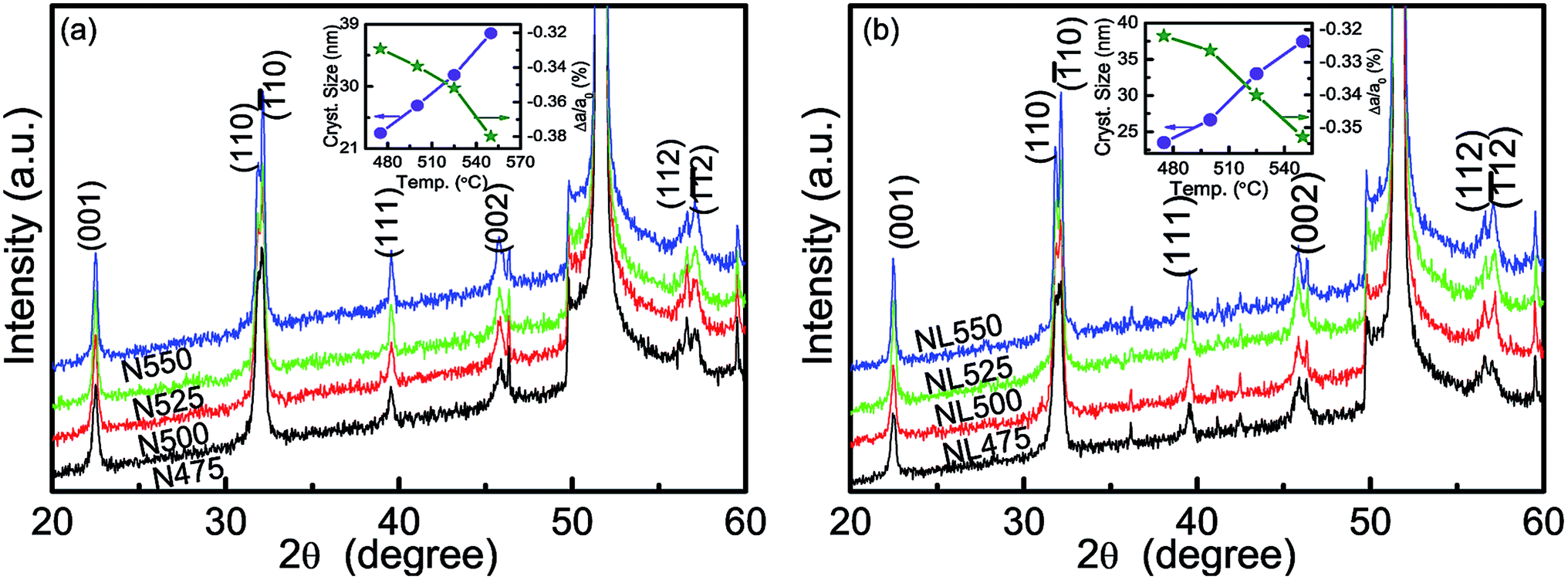 | ||
| Fig. 1 The XRD patterns of BFO thin films annealed at different temperatures: (a) BFO/Ni, and (b) BFO/LSTO/Ni. The variations in the averaged crystallite size and percentage change in lattice constant with the annealing temperature are shown in the corresponding insets. | ||
Considering the existing mismatch in thermal expansion coefficient and lattice constant between the BFO thin film and the metallic Ni tape, the strain induced by the substrate should be different in the BFO thin films at different annealing temperatures. The residual strain in the films can be reflected directly by the change in lattice constant. Here, the lattice constant of the BFO thin films is calculated with the parameters of the three most intense diffraction peaks, (001), (110) and (10), based on the pseudocubic structure. The percentage change in lattice constant (Δa = (a − a0)/a0% where a0 is taken as 0.397 nm (ref. 25)) of each thin film is calculated and plotted in the corresponding insets of Fig. 1. It can be seen that the percentage change in BFO lattice constant shows a negative value, and decreases slowly with increasing annealing temperature for both the BFO/Ni and BFO/LSTO/Ni thin films. The negative value indicates residual compressive strain in the obtained BFO thin films. The decreased negative value suggests that the compressive strain increases with the annealing temperature. As is commonly observed in CSD-derived thin films, grain growth may be responsible for the partial relaxation of microstrain.7,26 While, here, the BFO thin films with large crystallite size display high residual strain. It implies that the residual strain in BFO/Ni thin films cannot be relaxed via grain growth by increasing the annealing temperature. On the other hand, the BFO/LSTO/Ni thin films exhibit a smaller value of strain, suggesting that the introduction of a LSTO buffer layer is beneficial for residual strain relaxation.27 Considering the large thermal expansion coefficient mismatch between the BFO and Ni tape, a high compressive stress will be produced during the film’s cooling from the high annealing temperature. As a result, increased residual compressive strain is displayed with increasing annealing temperature. Additionally, due to the small thermal expansion coefficient mismatch between the BFO and LSTO, a small microstrain will be produced in the BFO/LSTO/Ni thin films, although both films exhibit a residual compressive microstrain on the same scale, as shown in the insets of Fig. 1.
Fig. 2 shows the surface FE-SEM images of all the obtained BFO thin films. It can be observed that the BFO grain size increases with increasing annealing temperature for both the BFO/Ni and BFO/LSTO/Ni thin films. Moreover, a different surface morphology between the BFO/Ni and BFO/LSTO/Ni thin films is exhibited, as shown in Fig. 2, which can be attributed to the different grain growth due to the introduction of a LSTO buffer layer. Additionally, the BFO/Ni thin films are prone to wrinkling. As displayed in the insets of Fig. 2(a1)–(d1), the wrinkle edges indicated by the arrows in the less magnified FE-SEM images are more visible. A clear interface layer without cracks is observed between the BFO layer and Ni tape from the FE-SEM image of the cross-section, as shown in the inset in the lower right corner of Fig. 2(d1)). Two clear interface layers are also observed between the BFO, LSTO, and Ni tape, as displayed in the inset of Fig. 2(d2), which indicates that LSTO acts as an effective barrier to possible atomic interdiffusion and reaction between the BFO thin film and Ni tape. Additionally, the wrinkles increase and grow gradually with increasing annealing temperature. Usually, shrinkages due to densification will occur during the heating process in CSD-derived films.28 At the same time, due to the hindrance of the viscous flow of the amorphous network associated with the substrate, strong tensile stresses parallel to the substrate will be induced, which can generate macroscopic heterogeneities, such as macrocracks or wrinkles.28 The appearance and increase of wrinkles are preserved in the films during crystallization at high temperatures. On the other hand, the introduction of a LSTO layer will relieve the hindrance caused by the metallic Ni tape. As a result, the wrinkles are smoothed in the BFO/LSTO/Ni thin films.
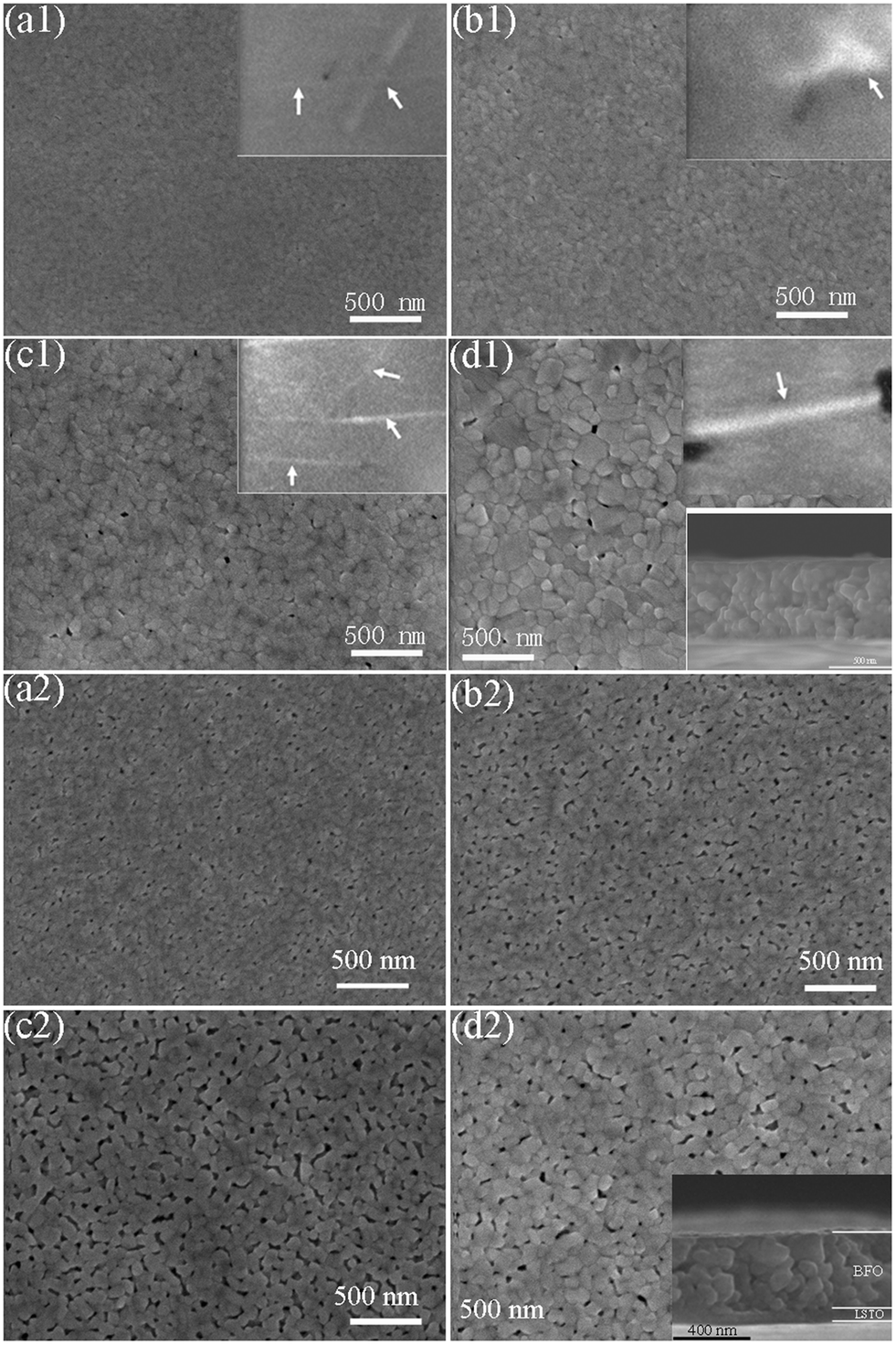 | ||
| Fig. 2 Surface FE-SEM images of the surface morphology of the BFO thin films ((a1)–(d1)) BFO/Ni, and ((a2)–(d2)) BFO/LSTO/Ni. The insets in the upper right corners of (a1)–(d1) show the less magnified FE-SEM images of the BFO/Ni films. Arrows indicate wrinkle edges. Insets in the lower right corners of (d1) and (d2) are the FE-SEM images of the cross-sections of two typical films N550 and NL550, respectively. | ||
3.2 Dielectric properties
The frequency dependent room temperature relative dielectric constants of all the obtained BFO thin films are shown in Fig. 3, and the dielectric losses of the corresponding films are displayed in the insets. The evolution of the dielectric constant measured at 1 MHz with the crystallite size is plotted in the inset of Fig. 3(b). It is seen that within the measured frequency range the dielectric constant increases while the dielectric loss decreases with increasing annealing temperature, which is the same as in our previous reports.6,7 On the other hand, the dielectric constant increases almost linearly with increasing crystallite size as shown in the inset of Fig. 3(b). Moreover, for each given annealing temperature the BFO/LSTO/Ni thin films show a larger dielectric constant. It is well known that there are intrinsic and extrinsic contributions to the dielectric permittivity in ferroelectric thin films.29,30 The thin film orientation and crystallite size are the most important factors.30 An increase in crystallite size will favor the formation of 180° domains, which can result in an enhanced dielectric constant.30 Here, all the BFO thin films show subtle changes related to the orientation with increasing annealing temperatures. However, the increase in crystallite size with increasing annealing temperature, as shown in Fig. 1 and 2, may favor the formation of the 180° domains, resulting in the enhancement of the dielectric constant. Additionally, as one of the extrinsic contributions to the dielectric permittivity, the grain boundary pinning and the mechanical strain/stress in the thin films can influence the dielectric response of the domain wall motion, and further affect the dielectric constant.7,29 With increasing annealing temperature, the decreased pinning caused by the decrease in grain boundaries will enhance the dielectric constant, although the increased microstrain, as shown in Fig. 1, will induce an inverse effect. For a given annealing temperature, the BFO/LSTO/Ni thin films have less microstrain, which will lead to weak pinning resulting in a larger dielectric constant. On the other side, the LSTO buffer layer may act as an effective barrier for interfacial layer formation due to atomic interdiffusion and reaction between the BFO thin film and the Ni tape during the annealing process. Normally, the interfacial layer will result in lowering of the dielectric constant due to its small permittivity.6 Thus, the increase in dielectric constant with an increased annealing temperature may have originated from the increased crystallite size and the decreased grain boundaries. The larger dielectric constant of the BFO/LSTO/Ni thin films is attributed to the decrease in pinning of the domain wall motion induced by the enhanced strain relaxation as well as the reduction in interfacial effects. The decreased dielectric loss with decreased annealing temperature, and introduction of a LSTO layer, may be caused by the decreased electrical conduction (leakage current), as shown below. | ||
| Fig. 3 Log-scaled frequency dependent room temperature relative dielectric constants of the BFO thin films (a) BFO/Ni, and (b) BFO/LSTO/Ni. The corresponding dielectric losses are shown in the insets of (a). The inset of (b) shows the variation of the dielectric constant measured at 1 MHz with crystallite size. | ||
3.3 Leakage properties
The leakage current density (J) at room temperature on a log scale as a function of electric field (E) for all obtained BFO thin films is shown in Fig. 4. J increases with increasing E, and the asymmetry can be attributed to the asymmetric electrodes.6 The J value increases with increasing annealing temperature for both the BFO/Ni and the BFO/LSTO/Ni thin films. The increase in J could be due to the increased oxygen vacancies due to the enhancement of crystallite size and the decrease in grain boundaries as discussed in our previous reports.6,7 In contrast, for a given annealing temperature, the J value of the BFO/LSTO/Ni thin films is much lower compared with that of the BFO/Ni thin films. It implies that the use of a LSTO buffer layer can improve the leakage properties in BFO thin films. The decrease in the leakage current density of the BFO/LSTO/Ni thin films is consistent with the fact that oxide electrodes can absorb oxygen vacancies.31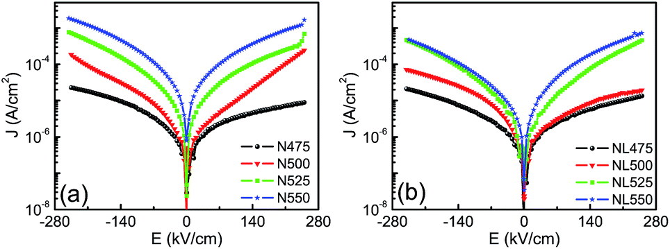 | ||
| Fig. 4 Room temperature leakage current density (J) on a log scale as a function of electric field (E) for the obtained BFO thin films (a) BFO/Ni, and (b) BFO/LSTO/Ni. | ||
3.4 Ferroelectric properties
Fig. 5 presents the evolution of the polarization with the applied electric field for all obtained BFO thin films. In fact, the thin films annealed at low temperatures show good ferroelectric hysteresis loops regardless of the use of the LSTO buffer layer. The higher the annealing temperature used, the lower the applied maximum electric field needed to obtain a ferroelectric hysteresis loop. Although the BFO/LSTO/Ni thin films annealed at low temperatures exhibit low maximum polarization, they display much better ferroelectric hysteresis loops with sharp shapes at the maximum electric fields. Additionally, as shown in Fig. 5, the coercive field (Ec, defined as the average electric field at zero polarization) derived from the polarization–electric field hysteresis loops decreases with increasing annealing temperature. Moreover, the value of Ec for the BFO/LSTO/Ni thin films is smaller than that of the BFO/Ni thin films. The decrease in Ec with increasing annealing temperature can be attributed to two factors. One is the decrease in individual-domain grains, induced by the enlarged grain size with increasing annealing temperature. The other is the reduced clamping of domain walls due to the decrease in grain boundaries with increasing annealing temperature. As discussed above, the crystallite size of the obtained BFO thin films is the same when a LSTO buffer layer is used or not used. Thus, the smaller Ec of the BFO/LSTO/Ni thin films does not originate from the variations in the individual-domain grains and clamping of domain walls. On the one side, as shown in Fig. 2 and the inset of Fig. 1, the wrinkles disappear and the microstrain is decreased in the BFO/LSTO/Ni thin films. Both factors will reduce the clamping of domain walls, resulting in the decreased Ec. On the other side, the decreased leakage current in the BFO thin films with a LSTO buffer layer, as shown in Fig. 4, suggests the decrease in oxygen vacancies, which act normally as the charge carriers in BFO. At the same time, the decrease in the oxygen vacancies can reduce the pinning of the domain walls motion,32 further leading to the lower Ec value. The reduced remnant polarization of the BFO/LSTO/Ni thin films should be caused by the same reasons. Additionally, the contribution of the leakage current to the polarization cannot be avoided in measurements of ferroelectric hysteresis loops,33 especially for the thin films with a high leakage value. The improved leakage of the BFO/LSTO/Ni thin films will also contribute to the decrease in the remnant and maximum polarizations.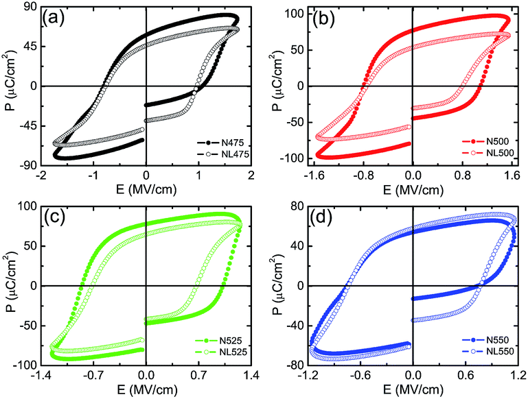 | ||
| Fig. 5 Evolution in polarization with applied electric fields for the BFO thin films, BFO/Ni and BFO/LSTO/Ni, annealed at different temperatures (a) 475, (b) 500, (c) 525, and (d) 550 °C. | ||
In order to eliminate the contribution of leakage current to the polarization as far as possible, a PUND measurement has been carried out with a varying field. The switched polarization (ΔP) values derived from these measurements are shown in Fig. 6. For each given annealing temperature, the field dependent ΔP of the obtained BFO thin films is displayed in the insets of Fig. 6. The switched polarization values ΔP derived from these measurements match well with the remnant polarization values obtained from the P–E loops. At a given applied electric field, ΔP increases initially and then decreases with increasing annealing temperature. The increase in the ΔP value is a result of two factors. One is the increase in multidomain grains as a consequence of grain growth with increasing annealing temperature. The other is the decreased pinning of the domain wall caused by the reduced grain boundary. However, the thin films, N550 and NL550, display lower ΔP values, which should be larger due to the larger crystallite size and fewer grain boundaries. Combining the microstrain and wrinkle results, the decreased ΔP can be attributed to the enhanced pinning or constraining of the polarization domain wall motion, caused by the increased compressive microstrain with increasing annealing temperature. Similarly, for each given annealing temperature, the reduced wrinkling and the low compressive microstrain32 may be the reasons for the large switched polarization of the derived BFO/LSTO/Ni thin films. On the other hand, the decreased oxygen vacancies as discussed above may be another reason, resulting in the decreased clamping of the domain walls.34 As a result, fewer domains are pinned, and a larger switching polarization value is exhibited. Generally, the variation of ferroelectric properties with annealing temperature is the result of the increased crystallite size and the microstrain, as well as the decreased grain boundaries. The crystallite size may be a major factor affecting the ferroelectric properties of the BFO/Ni thin films. For these thin films with the same crystallite size, the ferroelectric properties are affected by the thin film strain. The improved ferroelectric properties of the BFO/LSTO/Ni thin films are mainly caused by the smoothed wrinkles and the reduced microstrain as well as the improved leakage properties.
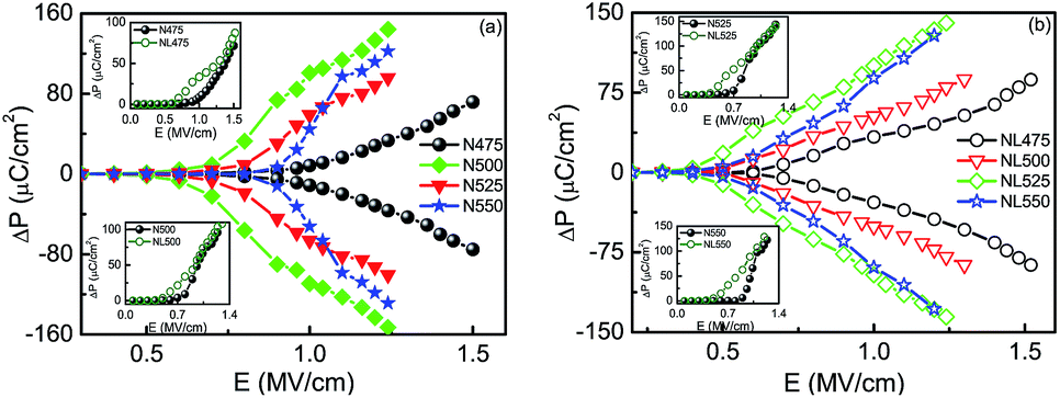 | ||
| Fig. 6 Switched polarization (ΔP) values at different maximum electric fields of the BFO thin films (a) BFO/Ni, and (b) BFO/LSTO/Ni. For a given annealing temperature, the field dependent ΔP values are shown in the inset. | ||
4 Conclusions
BFO thin films were prepared on metallic Ni tapes by chemical solution deposition. The effects of annealing temperature as well as the introduction of a LSTO buffer layer have been investigated systematically. With increasing annealing temperature, the crystallite size, the dielectric constant and the leakage current density are increased, while the coercive field is decreased. On the other hand, the microstrain is increased with increasing annealing temperature. The remnant polarization increases initially and then decreases with increasing annealing temperature. At each given annealing temperature, some wrinkles caused by the large mismatch in thermal expansion coefficient and lattice constant are observed in the BFO/Ni thin films, while they do not appear in the BFO/LSTO/Ni thin films. As a result, the BFO/LSTO/Ni thin films exhibit better ferroelectric hysteresis loops and smaller coercive fields, due to the smoothing of wrinkles and reduction of microstrain, as well as the improved leakage via the introduction of a LSTO buffer layer. These results will give a clear picture of the annealing temperature effects on the microstructure as well as the properties of CSD-derived BFO thin films on flexible Ni tapes. In addition, it will provide an instructive route to prepare and optimize the properties of BFO thin films on metallic tapes by the chemical solution deposition method.Acknowledgements
This work was supported by the National Science Foundation of China under Contract no.11204316.References
- Y. E. Roginskaya, Y. Y. Tomashpol'skii, Y. N. Venevtsev, V. M. Petrov and G. S. Zhdanov, Sov. Phys. JETP, 1966, 23, 47–51 Search PubMed.
- G. Catalan and J. F. Scott, Adv. Mater., 2009, 21, 2463–2485 CrossRef CAS.
- J. L. Wang, J. B. Neaton, H. Zheng, V. Nagarajan, S. B. Ogale, B. Liu, D. Viehland, V. Vaithyanathan, D. G. Schlom, U. V. Waghmare, N. A. Spaldin, K. M. Rabe, M. Wuttig and R. Ramesh, Science, 2003, 299, 1719–1722 CrossRef CAS PubMed.
- S. K. Singh, Y. K. Kim, H. Funakubo and H. Ishiwara, Appl. Phys. Lett., 2006, 88, 162904 CrossRef PubMed.
- S. Iakovlev, C. H. Solterbeck, M. Kuhnke and M. Es-Souni, J. Appl. Phys., 2005, 97, 094901 CrossRef PubMed.
- X. W. Tang, J. M. Dai, X. B. Zhu, J. C. Lin, Q. Chang, D. J. Wu, W. H. Song and Y. P. Sun, J. Am. Ceram. Soc., 2012, 95, 538–544 CrossRef CAS PubMed.
- X. W. Tang, X. B. Zhu, J. M. Dai and Y. P. Sun, Acta Mater., 2013, 61, 1739–1747 CrossRef CAS PubMed.
- J. T. Dawleya and P. G. Clem, Appl. Phys. Lett., 2002, 81, 3028 CrossRef PubMed.
- M. D. Losego, J. F. Ihlefeld and J. P. Maria, Chem. Mater., 2008, 20, 303–307 CrossRef CAS.
- J. Weaver, Z. Yuan, J. Liu, G. Collins, C. L. Chen, J. C. Jiang, J. He, E. I. Meletis, R. Y. Guo, A. Bhalla, B. Lin, V. Giiurgiutiu and M. W. Cole, Integr. Ferroelectr., 2008, 100, 61–71 CrossRef CAS.
- D. I. Woodward, I. M. Reaney, G. Y. Yang, E. C. Dickey and C. A. Randall, Appl. Phys. Lett., 2004, 84, 4650 CrossRef CAS PubMed.
- I. Bretos, T. Schneller, R. Waser, D. F. Hennings, S. Halder and F. Thomas, J. Am. Ceram. Soc., 2010, 93, 3983–3985 CrossRef PubMed.
- H. C. Lei, Y. P. Sun, X. B. Zhu, W. H. Song, J. Yang and H. W. Gu, IEEE Trans. Appl. Supercond., 2007, 17, 3819–3823 CrossRef CAS.
- L. Yan, M. Zhuo, Z. Wang, J. Yao, N. Haberkorn, S. Zhang, L. Civale, J. Li, D. Viehland and Q. X. Jia, Appl. Phys. Lett., 2012, 101, 012908 CrossRef PubMed.
- J. Shin, A. Goyal, S. Jesse and L. Heatherly, Appl. Phys. Express, 2011, 4, 021501 CrossRef.
- R. Y. Zheng, X. S. Gao, Z. H. Zhou and J. Wang, J. Appl. Phys., 2007, 101, 054104 CrossRef PubMed.
- Z. X. Cheng, H. Y. Zhao, Y. Du, H. Kimura, K. Ozawa and X. L. Wang, Scr. Mater., 2011, 65, 249–252 CrossRef CAS PubMed.
- Y. J. Qi, Z. H. Chen, C. W. Huang, L. H. Wang, X. D. Han, J. L. Wang, P. Yang, T. Sritharan and L. Chen, J. Appl. Phys., 2012, 111, 104117 CrossRef PubMed.
- M. S. Kartavtseva, O. Y. Gorbenko, A. R. Kaul, A. R. Akbashev, T. V. Murzina, S. Fusil, A. Barthlmy and F. Pailloux, Surf. Coat. Technol., 2007, 201, 9149–9153 CrossRef CAS PubMed.
- S. K. Singh, K. Maruyama and H. Ishiwara, Integr. Ferroelectr., 2008, 98, 83–89 CrossRef CAS.
- H. Naganuma and S. Okamura, J. Appl. Phys., 2007, 101, 09M103 CrossRef PubMed.
- S. K. Singh, H. Ishiwara and K. Maruyama, J. Appl. Phys., 2006, 100, 064102 CrossRef PubMed.
- R. W. Schwartz, Chem. Mater., 1997, 9, 2325–2340 CrossRef CAS.
- X. B. Zhu, S. B. Zhang, H. C. Lei, X. D. Zhu, G. Li, B. S. Wang, W. H. Song, Z. R. Yang, J. M. Dai, Y. P. Sun, D. Q. Shi and S. X. Do, J. Am. Ceram. Soc., 2009, 92, 800–804 CrossRef CAS PubMed.
- F. Tyholdt, H. Fjellvag, A. E. Gunsn and A. Olsen, J. Appl. Phys., 2007, 102, 074108 CrossRef PubMed.
- R. W. Schwartz, T. Schneller and R. Waser, C. R. Chim., 2004, 7, 433–461 CrossRef CAS PubMed.
- Y. Wang, Y. H. Lin and C. W. Nan, J. Appl. Phys., 2008, 104, 123912 CrossRef PubMed.
- K. Zalamova, N. Roma', A. Pomar, S. Morlens, T. Puig, J. Gazquez, A. E. Carrillo, F. Sandiumenge, S. Ricart, N. Mestres and X. Obradors, Chem. Mater., 2006, 18, 5897–5906 CrossRef CAS.
- F. Xu, S. T. McKinstry, W. Ren, B. M. Xu, Z. L. Xie and K. J. Hemker, J. Appl. Phys., 2001, 89, 1336 CrossRef CAS PubMed.
- J. P. Cruz, E. Joanni, P. M. Vilarinho and A. L. Kholkin, J. Appl. Phys., 2010, 108, 114106 CrossRef PubMed.
- B. Nagaraj, S. Aggarwal, T. K. Song, T. Sawhney and R. Ramesh, Phys. Rev. B: Condens. Matter Mater. Phys., 1999, 59, 16022–16027 CrossRef CAS.
- L. Jin, F. Li and S. J. Zhang, J. Am. Ceram. Soc., 2014, 97, 1–27 CrossRef CAS PubMed.
- M. Dawber, K. M. Rabe and J. F. Scott, Rev. Mod. Phys., 2005, 77, 1083–1130 CrossRef CAS.
- J. F. Scott and M. Dawber, Appl. Phys. Lett., 2000, 76, 3801–3803 CrossRef CAS PubMed.
| This journal is © The Royal Society of Chemistry 2014 |