Enhanced UV detection performance using a Cu-doped ZnO nanorod array film

Wen Dai, Xinhua Pan*, Cong Chen, Shanshan Chen, Wei Chen, Honghai Zhang and Zhizhen Ye*
State Key Laboratory of Silicon Materials, Cyrus Tang Center for Sensor Materials and Applications, Zhejiang University, Hangzhou 310027, P.R. China. E-mail: panxinhua@zju.edu.cn; yezz@zju.edu.cn; Fax: +86-571-87952124; Tel: +86-571-87952187

Received 7th May 2014 , Accepted 9th July 2014

First published on 9th July 2014


Abstract

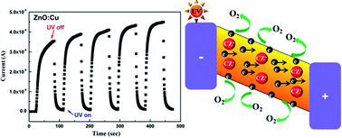
A compact Cu-doped ZnO nanorod (NR) array film was synthesized by a facile hydrothermal method and post-annealing process. The obtained ZnO NR array film-based UV photodetectors exhibit not only enhanced UV sensitivity but also faster reset time compared to undoped ZnO NR samples, which are attributed to the trapping and de-trapping of electrons by Cu-related defects.


Over the past decade, ultraviolet (UV) photodetectors have received extensive attention due to their various potential applications in many fields, including flame detection, space communication, pollution monitoring and military applications, etc.1–5 Generally, UV photodetectors with better quality factors, such as high UV sensitivity, fast response time, good reliability and low cost, are highly desirable for practical applications. Zinc oxide (ZnO), a typical n-type semiconductor with a wide direct band gap (3.37 eV at room temperature), has a large exciton binding energy of 60 meV compared to other wide band gap semiconductors.6 Therefore, ZnO is regarded as one of the most important materials for UV photodetection because of its unique characteristics such as high saturation drift velocity, strong radiation hardness, ease of manufacturing and low cost, etc. However, pure ZnO materials typically exhibit a relatively poor UV sensing performance due to the large n-type carrier concentration and fast recombination rate of photoexcited electron–hole pairs.7,8

To settle the above fundamental issues and improve the UV sensing properties of ZnO materials, defect engineering and doping processes have been applied to tailor certain properties of ZnO.9–12 More recently, copper (Cu) is regarded as one of the most effective dopants to enhance the UV sensing performance of ZnO, because the incorporation of Cu into ZnO can reduce the background carrier concentration which results in lower dark current.7,10,13 Furthermore, the radii of Cu2+ (73 pm) and Cu1+ (77 pm) ions are similar to Zn2+ (74 pm), and are thus more suitable for Zn2+ ion substitution compared to other doping ions. However, the role of Cu dopants in ZnO lattice is quite complicated due to the presence of various Cu-related complex defects. Therefore, it is necessary to further understand the photo-induced carrier behavior in Cu-doped ZnO. Many methods have been reported to synthesize Cu-doped ZnO, such as plasma-assisted molecular beam epitaxy (PA-MBE),14 sputtering,15 pulsed laser deposition (PLD),16 and vapor phase transport,17 which are relatively slow and expensive processes. Because of this, it is urgent to introduce a facile method with low cost, process simplicity, environmental friendliness and high yield of products to synthesize Cu-doped ZnO materials.

In this communication, we fabricated the Cu-doped ZnO nanorod (NR) array film by a simple hydrothermal method and post-annealing process. A reasonable formation mechanism is proposed to understand the morphological evolution between NR and NR array film after the introduction of Cu ions, which is closely related to the face-selective electrostatic adsorption and thermal diffusion of Cu ions. Moreover, the Cu-doped ZnO NR array film based UV photodetectors exhibit not only enhanced UV sensitivity but also faster reset time compared to undoped ZnO NR samples, which are closely related to the trapping and de-trapping of carriers by Cu-related defects. A model is also proposed to understand the complex photoconduction behavior in the Cu-doped ZnO NR array film.

The ZnO NR was synthesized via a facile hydrothermal method. Prior to the growth of ZnO NR array, a 30 nm ZnO seed layer was spin-coated on glass substrate (seed layer deposition details see ESI, Fig. S1). Afterwards, the seeded substrates were placed into a 100 mL growth solution containing 20 mM zinc acetate (Zn(CH3COO)2) and hexamethylenetetramine (C6H12N4, HMTA) at 90 °C for 4 h. For Cu doping, 2.5% copper acetate (Cu(CH3COO)2) (molar ratio of Cu precursor to ZnO precursor) was added into the growth solution to prepare Cu-doped ZnO NR array film. After the reaction was completed, the products were carefully cleaned with deionized water and ethanol several times followed by a drying step in an oven at 60 °C. Finally, post-annealing for 2 h at 400 °C in air atmosphere was performed for all samples.

The typical SEM images of ZnO NR and Cu-doped ZnO NR array film are shown in Fig. 1(a) and (b), respectively. The ZnO NR exhibits vertical, uniform, high-density NR arrays with an average diameter of 80 nm and a length of 1.5 μm, while the Cu-doped ZnO grains are also vertically aligned and fully coalesced throughout the film. It can be clearly seen that for Cu-doped ZnO, a much larger flat surface appears and the aspect ratio decreases considerably compared to that of undoped ZnO NR. These flat surfaces overlap with each other and coalesce to form a quasi-film (NR array film). With increasing the concentration of Cu ions, such change becomes more obvious (ESI, Fig. S2). The primary mechanism underlying the change of morphology is closely related to the face-selective electrostatic adsorption and thermal diffusion of Cu ions.18 By introducing Cu ions into the hydrothermal reaction, the Cu ions form complexes that can localize to the (0002) crystal surface of ZnO, thereby competitively limiting the access of the reactive zinc intermediates and inhibiting growth along the c-axis direction. Then, after thermal annealing at 400 °C, the electrostatic adsorbed Cu ions diffuse into the lattice site of ZnO and substitute Zn ions due to the similar ionic radii between Zn and Cu ions (see the description in ESI, Scheme S1). Fig. 1(c) depicts the XRD patterns of ZnO NR and Cu-doped ZnO NR array film. Except for one peak from the substrate, both samples show a very sharp (002) peak of wurtzite ZnO, which reveals that no Cu-related phases (Cu, CuO, or Cu2O) have been formed. To confirm the presence of Cu in the doped samples, the XPS measurement was carried out on the ZnO NR and Cu-doped ZnO NR array film, as shown in Fig. 1(d). No Cu related signal is found in ZnO NR, while strong Cu related signal is detected in the Cu-doped ZnO NR array film. Furthermore, the Cu 2p3/2 peak at 933.0 eV is asymmetric and can be deconvoluted into two peaks located at 932.6 eV and 933.6 eV, corresponding to Cu1+ and Cu2+ respectively (the inset of Fig. 1(d)).19,20 Thus, the presence of Cu in the doped samples is in Cu1+ and Cu2+ mixed state form.


image file: c4ra04249b-f1.tif
Fig. 1 Typical SEM images of (a) ZnO NR and (b) Cu-doped ZnO NR array film. The lengths of the scale bars are 200 nm for all images. (c) XRD patterns of ZnO NR and Cu-doped ZnO NR array film. (d) Cu 2p core-level XPS spectra of ZnO NR and Cu-doped ZnO NR array film. The inset shows the peak fitting of the Cu 2p3/2 peak.

For better understanding about the optical behavior of Cu dopants in ZnO, room temperature photoluminescence (PL) and PL excitation (PLE) measurements were performed, as shown in Fig. 2(a). It can be found that the Cu-doped sample exhibits a quite different PL spectrum compared with the pure one (the PL spectrum of pure ZnO NR see ESI, Fig. S3). The pure ZnO NR shows a strong near band emission and a weak broad visible emission. So far, there has been no consensus on the photoluminescence mechanism of the visible emission. It is generally considered that bulk defects such as oxygen vacancies may be responsible for this visible emission.21,22 While for Cu-doped ZnO NR array film, a huge visible emission dominates the whole PL spectrum, which seems to be related with the Cu doping. Moreover, the PLE spectra monitored at green-band (GB, peak at 500 nm) and yellow-band (YB, peak at 600 nm) emission are also quite different from each other. The YB PLE spectrum shows an onset close to 3.24 eV and a resonance at 3.37 eV. No other components occur at the low-energy side, indicating that the YB emission is mainly from intrinsic excitation of ZnO. On the contrary, besides the intrinsic excitation, the GB PLE spectrum also shows a Cu-related excitation band at the low-energy range, revealing a sub-bandgap light absorption and emission process.7 To further study the huge visible emission, the low-temperature (15 K) PL spectrum of the Cu-doped ZnO NR array film is given, showing a structured green emission (SGE) and a relatively strong YB, as shown in Fig. 2(b). The fine structures in SGE have an energy spacing of 72 meV, which is consistent with the longitudinal optical (LO) phonon replicas. The zero-phonon line for this SGE locates at 2.86 eV. Such features have been found in Cu doped ZnO.23 Meanwhile, the low-temperature PL spectrum of pure ZnO shows only a YB emission. Our data reconfirm that the GB emission is due to Cu transitions and the YB emission may be induced by the intrinsic defects in ZnO. And the extrapolated intercept of Cu-doped ZnO NR array film UV-vis absorbance spectrum on the photon energy axis yields a red-shifted optical band gap value compared with undoped ZnO NR (ESI, Fig. S4). Therefore, all above analyses indicate that Cu-related complex defects can be introduced into ZnO lattice through hydrothermal synthesis and post annealing process.


image file: c4ra04249b-f2.tif
Fig. 2 (a) Room temperature PL spectrum of Cu-doped ZnO NR array film, obtained by excitation by a 325 nm Xe lamp. Green and yellow solid lines represent the corresponding PLE spectra monitored at the peak of GB and YB, respectively. (b) PL spectra of ZnO NR and Cu-doped ZnO NR array film at 15 K.

The inset of Fig. 3(a) shows the structure illustration of the fabricated UV photodetector. The IV characteristics curves of the ZnO NR and the Cu-doped ZnO NR array film under dark conditions are shown in Fig. 3(a). The dark current of Cu-doped ZnO NR array is much smaller than that of ZnO NR, with the resistance increasing from 4.0 × 10⁷ to 2.0 × 10⁹ Ω. The Cu dopants in ZnO often act as a deep acceptor to trap electrons, thus the resistance of Cu-doped sample increases dramatically.13 The reduced dark current provides an opportunity to improve the UV sensitivity [sensitivity = (IphotoIdark)/Idark]. Fig. 3(b) and (c) show the time-resolved UV photocurrent on/off measurements of the ZnO NR and the Cu-doped ZnO NR array film at a bias of 5 V. As shown in Fig. 3(b) and (c), both devices show double exponential rise and decay under illumination. This indicates that two mechanisms may be attributed to the double exponential rise and decay, which widely exists in ZnO NRs based UV photodetectors.24,25 In Table 1, we review all parameters from the two devices. As compared with the undoped ZnO NR, the sensitivity of the Cu-doped ZnO NR array film has been improved more than one order of magnitude. Furthermore, the rise and decay time constants of the Cu-doped ZnO NR array film have been greatly decreased. Five repeated cycles are displayed in Fig. 3(d), in which the photocurrent is observed to be consistent and repeatable with no degenerate effect found during the detection process. Thereby, the Cu-doped ZnO NR array film greatly enhances the performance of UV detector. Moreover, our Cu-doped ZnO NR array film based UV photodetector shows similar performance to our previous reported polycrystalline ZnO: Cu-based film photodetector7 and much better UV sensing performance than other reported Cu-doped ZnO based UV photodetector.26


image file: c4ra04249b-f3.tif
Fig. 3 (a) IV characteristics curves of ZnO NR and Cu-doped ZnO NR array film under dark conditions, and the inset shows the schematic diagram of the fabricated UV detectors. The growth and decay of the photocurrent of ZnO NR and Cu-doped ZnO NR array film under 365 nm UV illumination: (b), (c) single-pulse and (d) multi-pulse observation.
Table 1 The parameters of the UV photodetectors fabricated from ZnO NR and Cu-doped ZnO NR array filma
Samples Idark (A) Iphoto (A) Sensitivity τg1 (s) τg2 (s) τd1 (s) τd2 (s)
a Sensitivity = (IphotoIdark)/Idark; τg1, τg2: 1st and 2nd growth time constant; τd1, τd2: 1st and 2nd decay time constant.
ZnO 1.3 × 10⁻⁷ 1.0 × 10⁻⁵ 76 2.2 23.7 4.5 35.5
ZnO:Cu 2.5 × 10⁻⁹ 5.2 × 10⁻⁶ 2080 1.9 7.3 0.9 4.1


Scheme 1 presents the scheme model of the Cu-doped ZnO NR array film based UV photodetector under dark and illumination conditions. When the ZnO NR was kept in the dark conditions, the oxygen molecules are absorbed on the surface of the ZnO NR by capturing free electrons from n-type ZnO NR [O2(g) + e → O2(ad)], leading to the formation of a high resistance region near the surface of ZnO NR. The electron–hole pairs are generated [ → e + h+] when the ZnO NR is illuminated by 365 nm UV light. The photogenerated holes oxidize the adsorbed oxygen molecules [O2(ad) + h+ → O2(g)] near the surface of ZnO NR; consequently, oxygen molecules are desorbed from the surface of ZnO NR, increasing free carrier concentration and producing a large photocurrent.5 However, for the Cu-doped ZnO NR array film, the adsorption and desorption of oxygen molecules are inefficient due to much decreased surface-to-volume ratio of the Cu-doped ZnO NR array film. In the dark conditions, Cu2+ usually acts as a deep acceptor trap center and interacts with native donors of ZnO to form [CuZn + Zni]0 complex which has been reported by West et al.,27 as shown in Scheme 1(a). Thus, the dark current is further decreased in the Cu-dope ZnO NR array film, as evidenced from the IV curves in Fig. 3(a). As shown in Scheme 1(b), when the Cu-doped ZnO NR array film is illuminated by 365 nm UV light, the [CuZn + Zni]0 complex is ionized to generate the [CuZn + Zni]+ complex and electrons, which produce a large photocurrent. Furthermore, the trapping and de-trapping of electrons by Cu-related complex defects are faster than the adsorption and desorption of oxygen molecules, which contributes to the faster reset time of the Cu-doped ZnO NR array film.28,29 Therefore, it is concluded that the enhanced UV sensing properties of the Cu-doped ZnO NR array film are mainly attributed to the trapping and de-trapping of electrons by Cu-related complex defects.


image file: c4ra04249b-s1.tif
Scheme 1 Schematic model to illustrate the mechanism of the high performance Cu-doped ZnO NR array film based UV photodetector.

In conclusion, Cu-doped ZnO NR array film has been synthesized for enhancing the UV detection performance by a facile hydrothermal method and post-annealing process. The PL and PLE measurements confirm the presence of Cu-related defects in ZnO NR. The Cu-doped ZnO NR array film based UV photodetector exhibits enhanced sensitivity and faster reset time. The enhanced UV sensing properties of the Cu-doped ZnO NR array film are mainly attributed to the trapping and de-trapping of electrons by Cu-related defects in ZnO NR. Through the introduction of Cu dopants into ZnO NR, a simple and efficient way is proposed to improve the UV sensing properties of ZnO NR.

Acknowledgements

This work was supported by National Natural Science Foundation of China under Grant nos 51302244 and 91333203, Zhejiang Provincial Public Technology Research of China under Grant no. 2012C21114, Zhejiang Provincial Natural Science Foundation of China under Grant no. LQ13E020001, and Doctoral Fund of Ministry of Education of China under Grant no. 2011010110013.

Notes and references

  1. S. Park, S. An, Y. Mun and C. Lee, Appl. Phys. A: Mater. Sci. Process., 2014, 114, 903–910 CrossRef CAS.
  2. K. Liu, M. Sakurai, M. Liao and M. Aono, J. Phys. Chem. C, 2010, 114, 19835–19839 CAS.
  3. X. Zhang, X. Han, J. Su, Q. Zhang and Y. Gao, Appl. Phys. A: Mater. Sci. Process., 2012, 107, 255–260 CrossRef CAS PubMed.
  4. W. Dai, X. H. Pan, S. S. Chen, C. Chen, Z. Wen, H. H. Zhang and Z. Z. Ye, J. Mater. Chem. C, 2014, 2, 4606–4614 RSC.
  5. C. Soci, A. Zhang, B. Xiang, S. A. Dayeh, D. P. R. Aplin, J. Park, X. Y. Bao, Y. H. Lo and D. Wang, Nano Lett., 2007, 7, 1003–1009 CrossRef CAS PubMed.
  6. W. Z. Lin, J. Phys.: Condens. Matter, 2004, 16, R829 CrossRef.
  7. L. Hu, L. Zhu, H. He, Y. Guo, G. Pan, J. Jiang, Y. Jin, L. Sun and Z. Ye, Nanoscale, 2013, 5, 9577–9581 RSC.
  8. T. Wang, Z. Jiao, T. Chen, Y. Li, W. Ren, S. Lin, G. Lu, J. Ye and Y. Bi, Nanoscale, 2013, 5, 7552–7557 RSC.
  9. Y. Li and X. Bi, Appl. Phys. A: Mater. Sci. Process., 2014, 114, 937–941 CrossRef CAS PubMed.
  10. C.-L. Hsu, Y.-D. Gao, Y.-S. Chen and T.-J. Hsueh, ACS Appl. Mater. Interfaces, 2014, 6, 4277–4285 CAS.
  11. S. Abd Aziz, S.-Y. Pung and Z. Lockman, Appl. Phys. A: Mater. Sci. Process., 2014, 1–11,  DOI:10.1007/s00339-014-8333-3.
  12. C.-L. Hsu, K.-C. Chen, T.-Y. Tsai and T.-J. Hsueh, Sens. Actuators, B, 2013, 182, 190–196 CrossRef CAS PubMed.
  13. R. Dingle, Phys. Rev. Lett., 1969, 23, 579–581 CrossRef CAS.
  14. J. B. Kim, D. Byun, S. Y. Ie, D. H. Park, W. K. Choi, C. Ji-Won and A. Basavaraj, Semicond. Sci. Technol., 2008, 23, 095004 CrossRef.
  15. H. Gong, J. Q. Hu, J. H. Wang, C. H. Ong and F. R. Zhu, Sens. Actuators, B, 2006, 115, 247–251 CrossRef CAS PubMed.
  16. D. B. Buchholz, R. P. H. Chang, J.-Y. Song and J. B. Ketterson, Appl. Phys. Lett., 2005, 87, 082504 CrossRef PubMed.
  17. G. Z. Xing, J. B. Yi, J. G. Tao, T. Liu, L. M. Wong, Z. Zhang, G. P. Li, S. J. Wang, J. Ding, T. C. Sum, C. H. A. Huan and T. Wu, Adv. Mater., 2008, 20, 3521–3527 CrossRef CAS.
  18. J. Joo, B. Y. Chow, M. Prakash, E. S. Boyden and J. M. Jacobson, Nat. Mater., 2011, 10, 596–601 CrossRef CAS PubMed.
  19. J.-L. Sun, J. Xu and J.-L. Zhu, Appl. Phys. Lett., 2007, 90, 201119 CrossRef PubMed.
  20. J. Cai and H. Gong, J. Appl. Phys., 2005, 98, 033707 CrossRef PubMed.
  21. A. B. Djurišić, Y. H. Leung, K. H. Tam, Y. F. Hsu, L. Ding, W. K. Ge, Y. C. Zhong, K. S. Wong, W. K. Chan, H. L. Tam, K. W. Cheah, W. M. Kwok and D. L. Phillips, Nanotechnology, 2007, 18, 095702 CrossRef.
  22. C. Ton-That, L. Weston and M. R. Phillips, Phys. Rev. B: Condens. Matter Mater. Phys., 2012, 86, 115205 CrossRef.
  23. N. Y. Garces, L. Wang, L. Bai, N. C. Giles, L. E. Halliburton and G. Cantwell, Appl. Phys. Lett., 2002, 81, 622–624 CrossRef CAS PubMed.
  24. R. Ghosh and D. Basak, Appl. Phys. Lett., 2007, 90, 243106 CrossRef PubMed.
  25. P.-N. Ni, C.-X. Shan, S.-P. Wang, X.-Y. Liu and D.-Z. Shen, J. Mater. Chem. C, 2013, 1, 4445–4449 RSC.
  26. S. Sarkar and D. Basak, Appl. Phys. Lett., 2013, 103, 041112 CrossRef PubMed.
  27. C. West, D. J. Robbins, P. J. Dean and W. Hayes, Physica B+C, 1983, 116, 492–499 CrossRef CAS.
  28. C. Shoou-Jinn, H. Ting-Jen, H. Cheng-Liang, L. Yan-Ru, I. C. Chen and H. Bohr-Ran, Nanotechnology, 2008, 19, 095505 CrossRef PubMed.
  29. J. S. Liu, C. X. Shan, B. H. Li, Z. Z. Zhang, C. L. Yang, D. Z. Shen and X. W. Fan, Appl. Phys. Lett., 2010, 97, 251102 CrossRef PubMed.

Footnote

Electronic supplementary information (ESI) available. See DOI: 10.1039/c4ra04249b

This journal is © The Royal Society of Chemistry 2014
Click here to see how this site uses Cookies. View our privacy policy here.