
Electronic and optical properties of silicene nanomeshes
Xue-Sheng Yea,
Zhi-Gang Shao*a,
Hongbo Zhaoa,
Lei Yangb and
Cang-Long Wangb
aLaboratory of Quantum Engineering and Quantum Materials, SPTE, South China Normal University, Guangzhou 510006, China. E-mail: zgshao@scnu.edu.cn
bChinese Academy of Sciences and Department of Physics, Institute of Modern Physics, Lanzhou University, Lanzhou 730000, China
First published on 1st August 2014
Abstract
We have investigated the electronic and optical properties of silicene nanomeshes (SNMs) using first-principle calculations. The emerging information indicates that the resulting properties are sensitive to the width (W) of the silicon chains between neighboring holes. Our results show that the bandgaps of SNMs with an odd W value remain closed. On the contrary, bandgaps are opened in SNMs with an even W value at the Γ points. Most importantly, SNMs possess a broad frequency photoresponse ranging from far infrared (0 eV) to ultraviolet (10 eV) and the optical properties of SNMs can be tuned by varying the value of W. Our results reveal that SNMs, as silicon-based materials, have a significant potential for electronic, photonic, and photovoltaic applications.
1 Introduction
Graphene, one of the most promising carbon-based materials with numerous potential applications, has been extensively studied since it was first obtained by Novoselov et al.,1,2 but cannot be used in transistor architectures because it is a semimetal with a closed bandgap.3–6 As a consequence, currently there is a surge in attempts to open the bandgap to make semimetallic graphene suitable for electronic applications, e.g. by being cut into nanoribbons,7–9 by applying a transverse electric field10–13 and by absorbing atoms in a regular pattern,14–19 and these methods meet particular nanotechnology challenges. Recently, graphene antidot lattices (i.e. graphene nanomeshes) have been first proposed by Pedersen et al.20 as a strategy to open the bandgap of graphene around the Fermi level. Since then, graphene nanomeshes have been extensively explored.3–6,20–30 Previous results show that the opened gap is associated with the size, shape, and symmetry of the nanomeshes.5,20–25,31,32 Exhilaratingly, essential experimental progresses in graphene nanomeshes have been achieved. Graphene nanomeshes have been successfully fabricated via electron beam lithography, block copolymer lithography, and self-assembly of mono-disperse colloidal microspheres.4,33–37Notably, Si, as a fundamental material, has played a key role in modern electronics industries. However, in photovoltaic industries, Si with an indirect bandgap of 1.1 eV (ref. 38) cannot make use of the energy below the gap.39 In addition, the carrier mobilities of Si are not balanced. The electron mobility (1400 cm2 v−1 s−1) is much larger than the hole mobility (450 cm2 v−1 s−1).40,41 The unbalanced charge-transport property results in hole accumulation42 in Si solar cell devices. Consequently, it reduces the photon to current conversion efficiency.43 Recently, silicene, the silicon-based counterpart of graphene with a linear dispersion of the band structure at the Fermi level, has been investigated quite intensively. Its extremely high carrier mobility makes it an ideal material, especially for electronic devices.44–50 It is useful for photovoltaic materials that the mobilities of the holes and electrons of silicene are in one order of magnitude (105 cm2 v−1 s−1).51 The more balanced transport of holes and electrons results in a better device performance.43 However, the pristine silicene is similar to graphene in that it lacks a band gap, which would be necessary for its use in transistor architectures.3–6,28,52
Therefore, in this work we introduce periodic holes in silicene to form silicene nanomeshes (SNMs) by first-principle calculations. Furthermore, we explore the electronic and optical properties of the SNMs via density functional theory.
2 Model and methods
The SNMs with periodically removed hexagonal silicon chains are shown in Fig. 1. The rhombus represents the super cell of the SNMs. W indicates the width of the silicon chains between the neighbouring holes. Each type of SNM is defined as {1,W}, with one removed hexagonal silicon chain (1) and the width (W) of the silicon chains between the neighboring holes.21 The dangling bonds are passivated by hydrogen. In the structures, the yellow and gray atoms represent silicon and hydrogen, respectively. The structural optimizations, band structures and optical spectra were calculated by first-principle calculations via the CASTEP code53–57 under periodic boundary conditions. The generalized gradient approximation (GGA) within the Perdew–Burke–Ernzerhof (PBE) exchange–correlation functional58 is employed to describe the exchange and correlation potentials. The Vanderbilt ultrasoft pseudopotential59 is used in the reciprocal space. The energy cutoff for the plane-wave expansion is set to 260 eV and 400 eV for the band structure and optical spectra calculations, respectively. The Monkhorst–Pack k-point mesh60 of 21 × 21 × 1 is set to provide sufficient accuracy in the Brillouin zone integration. SNM planes are separated by the vacuum of 16 Å in our calculations to avoid the effect of layers.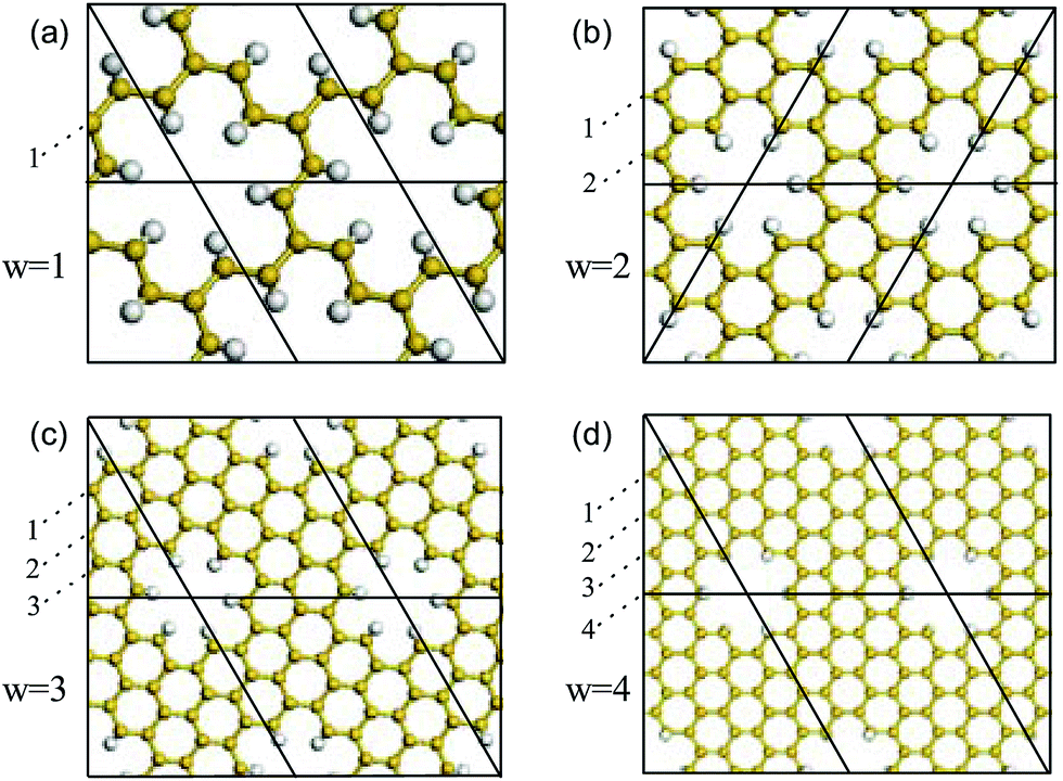 | ||
| Fig. 1 Structures of silicene nanomeshes (SNMs) with a varying width, W, in the silicon chains between the neighbouring holes, labeled as {1,1} (a), {1,2} (b), {1,3} (c), and {1,4} (d). The 1 in {1,W} represents a removed hexagonal silicon chain in the SNMs. In the structures, the yellow and gray atoms represent silicon and hydrogen, respectively. The numbers of the dashed lines illustrate the values of W. | ||
In the CASTEP calculations, the local field is not considered and therefore excitonic effects are not taken into account.53–57 The imaginary part of the dielectric constant can be expressed as:
 , where c is the speed of light and κ is the imaginary part of the refractive index,
  . In this work, we calculate the optical properties under unpolarized (U) and polarized (P) light conditions. E‖ polarization is defined if the electric field is parallel to the SNMs and the E⊥ polarization is defined if the electric field is perpendicular to the SNMs.63–65 We have only calculated the in-plane absorption since the SNMs are two-dimensional materials which are discontinuous in the perpendicular direction.65
3 Results and discussion
Fig. 2 illustrates the band structures of the SNMs calculated by the CASTEP code.53–57 After introducing the holes into silicene, the symmetry of the unit cell of the SNMs with an odd W value is reduced from P-3M1 (silicene) to P-3. However, the space group of the SNMs with an even W value changes from P-3M1 (silicene) to P-31M. But they still belong to the hexagonal group. Therefore, the area surrounded by the Γ–M–K–Γ path is the irreducible Brillouin zone of the two dimensional SNMs. As expected, the ones with an even W value have open bandgaps (0.64 eV and 0.32 eV for the {1,2} and {1,4} SNMs, respectively) around the Fermi level at the Γ points, as shown in Fig. 2(b) and (d). As far as we know, hydrogen passivation has a significant influence on the defects of silicene,66 but Pedersen et al. have proven that the antidot lattice, with regular holes in the graphene sheet, has important features as the size of the gap can be tuned via the antidot lattice parameters and the periodic perturbation turns the semimetal into a semiconductor.20 Compared to the SNMs with an odd value of W, it is found that SNMs with an even W value have a partially broken translational symmetry and the Dirac points are hybridized by the perforation and the passivated hydrogen,4,28,66–68 which lead to gaps.5,20–25,31,32,69,70 Hence, the energy gap opened in the SNMs results from the combination of quantum confinement and the periodic perturbation potential.22,25–28,69,70 Consequently, SNMs have a significant potential to be used as a transistor in logic applications and the small bandgap may be exploited to make new photonic devices for far infrared light detection. On the contrary, the SNMs with an odd W value remain semimetallic with Dirac cones in the Brillouin zone as shown in Fig. 2(a) and (c). Ouyang et al. have discussed that the closed bandgap at the k-point is related to the topological connection (bonding) between the carbon atoms in the graphene nanomeshes.21 In addition, the modulation behavior of the band gap, as a function of W in the SNMs, is similar to that in the graphene nanomeshes.21 Furthermore, we note that silicene has a linearly dispersing electronic band structure at the Fermi level, which contributes to its high carrier mobility.51 Though the introduced nanomeshes in silicene would reduce the mobilities of silicene, the valence band and the conduction band still preserve the symmetry and the linear dispersion around the Fermi level, as shown in Fig. 2. In this case, the high mobilities will still preserve well in the SNMs. Moreover, materials with higher mobilities can extremely improve the device performance. | ||
| Fig. 2 Band structures and density of states (DOS) of the {1,1} (a), {1,2} (b), {1,3} (c), and {1,4} (d) SNMs. | ||
Fig. 3 shows the imaginary part of the dielectric function, ε2(ω), of the SNMs. A striking difference between the optical spectra of the SNMs and Si is that, not only for the polarized light but also for the non-polarized light, ε2 of the SNMs has a nonzero value from a frequency of 0 eV, compared to that of Si which has a nonzero value from a frequency of 1.1 eV, which is the threshold for direct optical transitions between the valence band maximum and the conduction band minimum.71 In Fig. 3(a) and (b) the maximum values of ε2(ω) for the four types of SNMs lie within the visible to infrared part of the spectrum (<l eV) and the peak positions do not noticeably change for the unpolarized and the E‖ polarized light. But for the E‖ polarization, the height of the maximum values of ε2(ω) doubled compared to the non-polarization. However, a strong anisotropy in the imaginary part of the dielectric function is observed under E‖ and E⊥ polarization conditions. In the case of the E⊥ polarization for the four types of SNMs, the maximum values of ε2(ω) shift to a very high frequency region (∼8 eV).
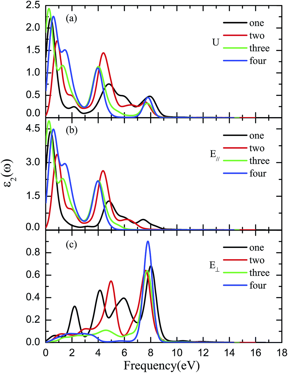 | ||
| Fig. 3 Imaginary part of the dielectric function ε2(ω) of the SNMs for unpolarized (U) (a) and E‖ (b) and E⊥ (c) polarized (P) light. The black, red, green, and blue lines correspond to {1,1}, {1,2}, {1,3}, and {1,4}, respectively. | ||
The real part of the dielectric function, ε1(ω), is shown in Fig. 4. It is found that Fig. 4(a) and (b) also show the same change tendency of ε1(ω) ranging from 0 eV to 6 eV, but the values of ε1(ω) in Fig. 4(b) are higher than the ones in Fig. 4(a) under polarized conditions. One important quantity of ε1(ω) is the zero frequency limit, ε1(0), which represents the dielectric response to the static electric field. Fig. 4(a) and (b) show the inverse relationship between the band gap and ε1(0). A smaller energy gap yields a larger ε1(0) value.71,72 This can be understood based on the equation  .71,72 In Fig. 4(b), ε1(0) describes the varying values ranging from 4.56 to 14.81 for the four types of SNMs under the polarized condition. A higher value in the static dielectric constants leads to larger available free charge carriers.61 For example, in Fig. 4(b) under E‖ polarization conditions the two types of SNMs ({1,1} and {1,3}) with Dirac points have higher values of 11.51 and 14.81, respectively. However, the SNM with W = 2 is a semiconductor with a larger bandgap about 0.64 eV and a lower corresponding ε1(0) value of 4.56 for the E‖ polarized light.
 | ||
| Fig. 4 Real part of the dielectric function, ε1(ω), of the SNMs for unpolarized (U) (a) and E‖ (b) and E⊥ (c) polarized light. The black, red, green, and blue lines correspond to {1,1}, {1,2}, {1,3}, and {1,4}, respectively. | ||
Fig. 5 describes the absorption spectra, which indicate the fraction of the energy lost by the light wave when it passes through the material.57 It is clearly found that the absorption coefficients of the four types of SNMs have nonzero values from 0 eV under E‖ polarized and unpolarized light conditions. They absorb light of different frequencies as W varies. It is obvious that the absorption spectra below 1 eV more intuitively correspond to the band structure of the four types of the SNMs around the Fermi level. SNMs with an odd W value reserve the Dirac cones, but their Dirac cones with larger W values become more flat, as shown in Fig. 2(a) and (c). The bandgap of the SNMs decreases as the value of the even W values increases. Therefore, a red shift appears in the absorption spectra of the SNM with W = 3 compared to the one with W = 1, and in the spectra of the one with W = 4 compared to the one with W = 2. In Fig. 5(a), under unpolarized light conditions, the four types of SMNs have three prominent peaks around 2 eV, 4.5 eV, and 8 eV, respectively. The first peak of the four types moves from the far infrared zone to the visible light zone, and the peak values locate from 1 eV to 2 eV as the corresponding W value varies from 1 to 4. In Fig. 5(b), under E‖ polarization light conditions, the four types of SNMs lack the third peak as shown in Fig. 5(a). However, under E⊥ polarization conditions, the four types of SNMs only preserve the third prominent peak around 8 eV. In Fig. 5(a)–(c) it can be easily seen that the absorption spectra are enhanced under polarization conditions compared to under non-polarization conditions. But the SNMs prefer to absorb the E‖ polarized light below 6 eV, while the SNMs only absorb the E⊥ polarized light around 8 eV.
 | ||
| Fig. 5 Absorption coefficients of the SNMs for unpolarized (a) and E‖ (b) and E⊥ (c) polarized light. The black, red, green, and blue lines correspond to {1,1}, {1,2}, {1,3}, and {1,4}, respectively. | ||
Moreover, Fig. 3–5 all reveal that the optical properties of the SNMs are sensitive to the value of W. Our results show that the SNMs possess a broad frequency photoresponse ranging from 0 eV to 10 eV. We note that a limitation of Si is that it has a band gap of 1.1 eV, which means that photons with an energy below the bandgap are lost.39,73 Nevertheless, the SNMs can make full use of the solar energy below 1.1 eV. If an SNM-based solar cell can be developed, the utilization of sunlight will be extremely improved. Furthermore, SNMs can be exploited to make new photonic devices for far infrared light detection with an absorption from 0 eV.65 In addition, a strong anisotropy in the optical properties is also observed, which is in contrast to the fact that Si is optically isotropic. Polarized dependent optical spectra would make the SNMs more versatile than Si in potential applications.
4 Conclusions
In summary, we have investigated the electronic and optical properties of SNMs. Our results show that the electronic and optical properties of SNMs are extremely sensitive to the W value of the silicon chains between the neighboring holes. The bandgap of the SMNs with an odd W value remains closed. On the contrary, substantial bandgaps are opened in SMNs with an even W value around the Fermi level. Hence, SNMs have a significant potential for applications in electronics, and the SNMs with an even W value, which are semiconductors, can be used for effective field-effect transistors operating at room temperature. SNMs also can be exploited to make new photonic devices for far infrared light detection with an absorption from 0 eV. In addition, our results show that the optical properties of the SNMs are anisotropic under E‖ and E⊥ polarized conditions. Furthermore, the optical properties of the SNMs can be tuned by varying W. SNMs, possessing a broad frequency photoresponse ranging from 0 eV to the ultra-violet region 10 eV, can be used for solar energy. Since photovoltaics can make a considerable contribution to solving the energy problem that our society faces,39 SNMs may pave a possible way towards solar cell materials.Acknowledgements
Zhi-Gang Shao acknowledges the support by the National Natural Science Foundation of China (Grant no. 11105054 and 11274124), PCSIRT (Grant no. IRT1243), China Scholarship Council, and by the high-performance computing platform of South China Normal University. Hongbo Zhao acknowledges the support by the National Natural Science Foundation of China (Grant no. 91026005). Lei Yang acknowledges the support by the “Strategic Priority Research Program” of the Chinese Academy of Sciences (Grant no. XDA03030100). Cang-Long Wang acknowledges the support by the National Natural Science Foundation of China (Grant no. 11304324).References
- K. S. Novoselov, A. K. Geim, S. V. Morozov, D. Jiang, Y. Zhang, S. V. Dubonos, I. V. Grigorieva and A. A. Frisov, Science, 2004, 306, 666–669 CrossRef CAS PubMed.
- K. S. Novoselov, A. K. Geim, S. V. Morozov, D. Jiang, M. I. Katsnelson, I. V. Grigorieva, S. V. Dubonos and A. A. Frisov, Nature, 2005, 438, 197 CrossRef CAS PubMed.
- R. Martinazzo, S. Casolo and G. F. Tantardini, Phys. Rev. B: Condens. Matter Mater. Phys., 2010, 81, 245420 CrossRef.
- J. Bai, X. Zhong, S. Jiang, Y. Huang and X. Duan, Nat. Nanotechnol., 2010, 5, 190–194 CrossRef CAS PubMed.
- R. Petersen, T. G. Pedersen and A.-P. Jauho, ACS Nano, 2011, 5, 523–529 CrossRef CAS PubMed.
- S. Yuan, R. Roldán, A.-P. Jauho and M. I. Katsnelson, Phys. Rev. B: Condens. Matter Mater. Phys., 2013, 87, 085430 CrossRef.
- M. Y. Han, B. Özyilmaz, Y. Zhang and P. Kim, Phys. Rev. Lett., 2007, 98, 206805 CrossRef.
- Y.-W. Son, M. L. Cohen and S. G. Louie, Phys. Rev. Lett., 2006, 97, 216803 CrossRef.
- L. Brey and H. A. Fertig, Phys. Rev. B: Condens. Matter Mater. Phys., 2006, 73, 235411 CrossRef.
- E. V. Castro, K. S. Novoselov, S. V. Morozov, N. M. R. Peres, J. M. B. L. dos Santos, J. Nilsson, F. Guinea, A. K. Geim and A. H. C. Neto, Phys. Rev. Lett., 2007, 99, 216802 CrossRef.
- E. McCann, Phys. Rev. B: Condens. Matter Mater. Phys., 2006, 74, 161403 CrossRef.
- A. Deshpande, W. Bao, Z. Zhao, C. N. Lau and B. J. LeRoy, Appl. Phys. Lett., 2009, 95, 243502 CrossRef PubMed.
- Z. Ni, Q. Liu, K. Tang, J. Zheng, J. Zhou, R. Qin, Z. Gao, D. Yu and J. Lu, Nano Lett., 2012, 12, 113–118 CrossRef CAS PubMed.
- R. Balog, B. Jorgensen, L. Nilsson, M. Andersen, E. Rienks, M. Bianchi, M. Fanetti, E. Laegsgaard, A. Baraldi, S. Lizzit, Z. Sljivancanin, F. Besenbacher, B. Hammer, T. G. Pedersen, P. Hofmann and L. Hornekaer, Nat. Mater., 2010, 9, 315–319 CrossRef CAS PubMed.
- J. O. Sofo, A. S. Chaudhari and G. D. Barber, Phys. Rev. B: Condens. Matter Mater. Phys., 2007, 75, 153401 CrossRef.
- L. Liu and Z. Shen, Appl. Phys. Lett., 2009, 95, 252104 CrossRef PubMed.
- X.-L. Wei, H. Fang, R.-Z. Wang, Y.-P. Chen and J.-X. Zhong, Appl. Phys. Lett., 2011, 99, 012107 CrossRef PubMed.
- X. Liu, Y. Wen, Z. Chen, H. Lin, R. Chen, K. Cho and B. Shan, AIP Adv., 2013, 3, 052126 CrossRef PubMed.
- R. Wang, X. Pi, Z. Ni, Y. Liu, S. Lin, M. Xu and D. Yang, Sci. Rep., 2013, 3, 1–6 Search PubMed.
- T. G. Pedersen, C. Flindt, J. Pedersen, N. A. Mortensen, A.-P. Jauho and K. Pedersen, Phys. Rev. Lett., 2008, 100, 136804 CrossRef.
- F. Ouyang, S. Peng, Z. Liu and Z. Liu, ACS Nano, 2011, 5, 4023–4030 CrossRef CAS PubMed.
- J. Lee, A. K. Roy, J. L. Wohlwend, V. Varshney, J. B. Ferguson, W. C. Mitchel and B. L. Farmer, Appl. Phys. Lett., 2013, 102, 203107 CrossRef PubMed.
- F. Ouyang, Z. Yang, S. Peng, X. Zheng and X. Xiong, Phys. E, 2014, 56, 222–226 CrossRef CAS PubMed.
- X. Y. Cui, R. K. Zheng, Z. W. Liu, L. Li, B. Delley, C. Stampfl and S. P. Ringer, Phys. Rev. B: Condens. Matter Mater. Phys., 2011, 84, 125410 CrossRef.
- H. Jippo, M. Ohfuchi and C. Kaneta, Phys. Rev. B: Condens. Matter Mater. Phys., 2011, 84, 075467 CrossRef.
- M. H. Schultz, A. P. Jauho and T. G. Pedersen, Phys. Rev. B: Condens. Matter Mater. Phys., 2011, 84, 045428 CrossRef.
- C.-H. Park, L. Yang, Y.-W. Son, M. L. Cohen and S. G. Louie, Phys. Rev. Lett., 2008, 101, 126804 CrossRef.
- K. Lopata, R. Thorpe, S. Pistinner, X. Duan and D. Neuhauser, Chem. Phys. Lett., 2010, 498, 334–337 CrossRef CAS PubMed.
- W. Oswald and Z. Wu, Phys. Rev. B: Condens. Matter Mater. Phys., 2012, 85, 115431 CrossRef.
- H. Şahin and S. Ciraci, Phys. Rev. B: Condens. Matter Mater. Phys., 2011, 84, 035452 CrossRef.
- J. A. Fürst, T. G. Pedersen, M. Brandbyge and A.-P. Jauho, Phys. Rev. B: Condens. Matter Mater. Phys., 2009, 80, 115117 CrossRef.
- H. Y. He, Y. Zhang and B. C. Pan, J. Appl. Phys., 2010, 107, 114322 CrossRef PubMed.
- M. Kim, N. S. Safron, E. Han, M. S. Arnold and P. Gopalan, Nano Lett., 2010, 10, 1125–1131 CrossRef CAS PubMed.
- X. Liang, Y.-S. Jung, S. Wu, A. Ismach, D. L. Olynick, S. Cabrini and J. Bokor, Nano Lett., 2010, 10, 2454–2460 CrossRef CAS PubMed.
- T. Shen, Y. Q. Wu, M. A. Capano, L. P. Rokhinson, L. W. Engel and P. D. Ye, Appl. Phys. Lett., 2008, 93, 122102 CrossRef PubMed.
- S. Heydrich, M. Hirmer, C. Preis, T. Korn, J. Eroms, D. Weiss and C. Schüller, Appl. Phys. Lett., 2010, 97, 043113 CrossRef PubMed.
- A. Sinitskii and J. M. Tour, J. Am. Chem. Soc., 2010, 132, 14730–14732 CrossRef CAS PubMed.
- J. D. Holmes, K. P. Johnston, R. C. Doty and B. A. Korgel, Science, 2000, 287, 1471–1473 CrossRef CAS.
- H. A. Atwater and A. Polman, Nat. Mater., 2010, 9, 205–213 CrossRef CAS PubMed.
- G. W. Ludwig and R. L. Watters, Phys. Rev., 1956, 101, 1699–1701 CrossRef CAS.
- M. B. Prince, Phys. Rev., 1954, 93, 1204–1206 CrossRef CAS.
- C. Melzer, E. J. Koop, V. D. Mihailetchi and P. W. M. Blom, Adv. Funct. Mater., 2004, 14, 865–870 CrossRef CAS PubMed.
- G. Li, V. Shrotriya, J. Huang, Y. Yao, T. Moriarty, K. Emery and Y. Yang, Nat. Mater., 2005, 4, 864–868 CrossRef CAS.
- P. De Padova, C. Quaresima, C. Ottaviani, P. M. Sheverdyaeva, P. Moras, C. Carbone, D. Topwal, B. Olivieri, A. Kara, H. Oughaddou, B. Aufray and G. Le Lay, Appl. Phys. Lett., 2010, 96, 261905 CrossRef PubMed.
- B. Lalmi, H. Oughaddou, H. Enriquez, A. Kara, S. Vizzini, B. Ealet and B. Aufray, Appl. Phys. Lett., 2010, 97, 223109 CrossRef PubMed.
- S. Cahangirov, M. Topsakal, E. Aktürk, H. Şahin and S. Ciraci, Phys. Rev. Lett., 2009, 102, 236804 CrossRef CAS.
- C.-C. Liu, W. Feng and Y. Yao, Phys. Rev. Lett., 2011, 107, 076802 CrossRef.
- G. G. Guzmán-Verri and L. C. Lew Yan Voon, Phys. Rev. B: Condens. Matter Mater. Phys., 2007, 76, 075131 CrossRef.
- F.-B. Zheng, C.-W. Zhang, P.-J. Wang and S.-S. Li, J. Appl. Phys., 2013, 113, 154302 CrossRef PubMed.
- T. P. Kaloni, Y. C. Cheng and U. Schwingenschlögl, J. Appl. Phys., 2013, 113, 104305 CrossRef PubMed.
- Z.-G. Shao, X.-S. Ye, L. Yang and C.-L. Wang, J. Appl. Phys., 2013, 114, 093712 CrossRef PubMed.
- M. L. Trolle, U. S. Møller and T. G. Pedersen, Phys. Rev. B: Condens. Matter Mater. Phys., 2013, 88, 195418 CrossRef.
- M. D. Segall, P. J. D. Lindan, M. J. Probert, C. J. Pickard, P. J. Hasnip, S. J. Clark and M. C. Payne, J. Phys.: Condens. Matter, 2002, 14, 2717 CrossRef CAS.
- P. Hohenberg and W. Kohn, Phys. Rev., 1964, 136, B864–B871 CrossRef.
- W. Kohn and L. J. Sham, Phys. Rev., 1965, 140, A1133–A1138 CrossRef.
- M. C. Payne, M. P. Teter, D. C. Allan, T. Arias and J. D. Joannopoulos, Rev. Mod. Phys., 1992, 64, 1045–1097 CrossRef CAS.
- S. J. Clark, M. D. Segall, C. J. Pickard, P. J. Hasnip, M. J. Probert, K. Refson and M. Payne, Z. Kristallogr., 2005, 220, 567–570 CAS.
- J. P. Perdew, K. Burke and M. Ernzerhof, Phys. Rev. Lett., 1996, 77, 3865–3868 CrossRef CAS.
- D. Vanderbilt, Phys. Rev. B: Condens. Matter Mater. Phys., 1990, 41, 7892–7895 CrossRef.
- J. D. Monkhorst and H. J. Pack, Phys. Rev. B: Condens. Matter Mater. Phys., 1976, 13, 5188–5192 CrossRef.
- S. Kumar Jain and P. Srivastava, J. Appl. Phys., 2013, 114, 073514 CrossRef PubMed.
- N. Singh, T. P. Kaloni and U. Schwingenschlögl, Appl. Phys. Lett., 2013, 102, 023101 CrossRef PubMed.
- J. Kang, J. Li, F. Wu, S.-S. Li and J.-B. Xia, J. Phys. Chem. C, 2011, 115, 20466–20470 CAS.
- Y. Liu, H. Shu, P. Liang, D. Cao, X. Chen and W. Lu, J. Appl. Phys., 2013, 114, 20466–20470 Search PubMed.
- L. Matthes, P. Gori, O. Pulci and F. Bechstedt, Phys. Rev. B: Condens. Matter Mater. Phys., 2013, 87, 035438 CrossRef.
- J. Gao, J. Zhang, H. Liu, Q. Zhang and J. Zhao, Nanoscale, 2013, 5, 9785–9792 RSC.
- T. H. Osborn, A. A. Farajian, O. V. Pupysheva, R. S. Aga and L. L. Y. Voon, Chem. Phys. Lett., 2011, 511, 101–105 CrossRef CAS PubMed.
- E. Bekaroglu, M. Topsakal, S. Cahangirov and S. Ciraci, Phys. Rev. B: Condens. Matter Mater. Phys., 2010, 81, 075433 CrossRef.
- C.-L. Lin, R. Arafune, K. Kawahara, M. Kanno, N. Tsukahara, E. Minamitani, Y. Kim, M. Kawai and N. Takagi, Phys. Rev. Lett., 2013, 110, 076801 CrossRef.
- Y.-L. Song, Y. Zhang, J.-M. Zhang, D.-B. Lu and K.-W. Xu, J. Mol. Struct., 2011, 990, 75–78 CrossRef CAS PubMed.
- L. Guo, S. Zhang, W. Feng, G. Hu and W. Li, J. Alloys Compd., 2013, 579, 583–593 CrossRef CAS PubMed.
- D. R. Penn, Phys. Rev., 1962, 128, 2093–2097 CrossRef CAS.
- C. Solanki and G. Beaucarne, Energy Sustainable Dev., 2007, 11, 17–23 CrossRef CAS.
| This journal is © The Royal Society of Chemistry 2014 |