Vapour-based processing of hole-conductor-free CH3NH3PbI3 perovskite/C60 fullerene planar solar cells†
Hao Huac,
Dong Wangac,
Yuanyuan Zhoub,
Jiliang Zhangd,
Siliu Lva,
Shuping Pang*a,
Xiao Chena,
Zhihong Liua,
Nitin P. Padtureb and
Guanglei Cui*a
aQingdao Institute of Bioenergy and Bioprocess Technology, Chinese Academy of Sciences, Qingdao 266101, P.R. China
bSchool of Engineering, Brown University, Providence, RI 02912, USA
cUniversity of Chinese Academy of Sciences, Beijing 100049, P. R. China
dDepartment of Physics and Materials Science, City University of Hong Kong, SAR, Hong Kong
First published on 19th June 2014
Abstract
A new sequential-vapour-deposition method is demonstrated for the growth of high-quality CH3NH3PbI3 perovskite films. This has enabled the all-vapour, low-temperature fabrication of hole-conductor-free planar perovskite solar cells consisting of only a CH3NH3PbI3/C60 bi-layer sandwiched between two electrical contacts, with a power conversion efficiency of 5.4%.
Organometallic trihalide perovskites with the general formula (RNH3)MeX3 (where R is an organic group, Me is Pb or Sn, and X is a halogen I, Br, or Cl) have recently emerged as new generation light harvesting materials in excitonic solar cells.1–3 In particular, methylammonium (MA) lead triiodide (CH3NH3PbI3 or MAPbI3) has attracted great deal of attention since it was first applied as the light absorber in mesoscopic solar cells.4–6 Within a short period of time the power conversion efficiency (PCE) of MAPbI3-based solar cells has shot up dramatically to 16.2%.4,6,7 This rapid rise in the performance is the result of the innate desirable properties of MAPbI3, including favourable direct band gap, large adsorption coefficient, high carrier mobilities and long carrier (balanced) diffusion lengths.1,5,6,8 With regards to the latter, Xing et al.8 showed that the carrier diffusion length in solution-processed MAPbI3 thin films is at least 100 nm, despite the non-ideal nature of the solution-spun MAPbI3 films. Higher PCEs of ∼12% were obtained by Malinkiewicz et al.9 and Chen et al.10 in planar (non-mesoscopic) solar cells based on better quality MAPbI3 films of ∼300 nm thickness. This suggests that maximizing the quality (coverage, crystallinity, texture) of MAPbI3 films can lead to carriers diffusion lengths >300 nm, which is the key to realizing planar perovskite-based solar cells with high efficiencies.8,9
However, reliable deposition of high-quality films of phase-pure MAPbI3 perovskites with full coverage and high crystallinity still remains a challenge.5,6 One-step solution-spun MAPbI3 generally results in films with pinholes due to high reaction rate between MAI and PbI2.4,10 To address this issue Burschka, et al.4 developed a two-step method, where mesoporous TiO2 is first infiltrated by solution-processed PbI2, followed by dipping it in a MAI solution for the in situ formation of MAPbI3. However, in the case of planar solar cells, where a mesoporous TiO2 scaffold is not used, several hours are needed for the complete conversion of MAPbI3, which can result in the peeling of the films.4 In another study involving planar solar cells, the dipping process was replaced by extended annealing of the solution-processed PbI2 film in a MAI-vapour-rich N2 atmosphere at 150 °C.10 However, this process may be not amenable to producing uniform MAPbI3 films on organic substrates.10 Meanwhile, Liu et al.11 and Malinkiewicz et al.9 used dual-source co-evaporation deposition to prepare uniform, pinhole-free films of MAPbI3 or chorine-doped MAPbI3, where the resulting planar solar cells delivered one of the highest PCEs. However, careful control of evaporation rates of the organic and the inorganic precursors is needed to achieve proper stoichiometry in the deposited films.
To that end, we demonstrate here a facile sequential-vapour-deposition (SVD) approach for the growth of high-quality MAPbI3 films, which has enabled the fabrication of simple perovskite-based planar solar cells consisting of a MAPbI3 perovskite/C60 fullerene bi-layer sandwiched between two electrical contacts (indium tin oxide (ITO) coated glass and thermally-evaporated Ag). A maximum PCE of 5.4% is achieved in these solar cells. To our knowledge, this type of bi-layer architecture, which is devoid of any additional blocking layer, any mesoporous scaffold (e.g. TiO2, ZnO, or Al2O3), and any additional conducting organic layers, constitutes the simplest perovskite-based working solar cell reported thus far. Especially, while several groups have hole-conductor-free mesoscopic perovskite solar cells, this is the first report of planar perovskite solar cells without use of hole conductors.
Fig. 1 is a schematic diagram of the SVD method for the growth of MAPbI3 films. A nanostructured porous PbI2 film is first vapour-deposited (Fig. 1A), followed by the vapour-deposition of MAI (Fig. 1B), which reacts in situ with the PbI2 film (Fig. 1C). The freshly prepared MAPbI3 film is further annealed at 100 °C for 30 min to produce a textured film (Fig. 1D). Note that strong texture in perovskite films have been suggested to be beneficial, most likely due to their improved carriers-transport properties.12,13
 | ||
| Fig. 1 Schematic representation of the sequential-vapour deposition (SVD) process for the growth of MAPbI3 perovskite films. | ||
Detailed experimental procedures, including SVD growth of the films and solar cells fabrication, are presented in the accompanying (ESI†). Also presented in ESI are characterization procedures, including X-ray diffractometry (XRD), scanning electron microscopy (SEM), optical microscopy and ultraviolet-visible (UV-vis) optical spectroscopy, and procedures for solar cells testing.
Fig. 2 shows XRD patterns from the films at different stages of the SVD growth, and the evolution of the surface morphology of the thin films. The XRD pattern in Fig. 2A confirms the presence of layered PbI2 (space group P3m1; a = 4.600(2) Å, b = 4.600(2) Å, c = 6.9926(9) Å) in the film after the first step, and shows a strong 001 texture. The corresponding SEM image in Fig. 2B shows full-coverage, smooth film consisting of randomly-oriented packing of plate-like PbI2. There is some amount of porosity between the adjacent PbI2 plates in the film. The thickness of the PbI2 plate-like structures is estimated at ∼20–30 nm (see Fig. S1 in ESI†), which is responsible for the broadening of the XRD peaks in Fig. 2A. In contrast, solution-processed PbI2 films prepared by spin-coating are relatively rough, with equiaxed grains of PbI2 of few hundred nanometers size.4 Fig. 2C is XRD pattern of PbI2 film exposed to MAI vapour for 5 min, showing the presence of both PbI2 and MAPbI3. The corresponding SEM image in Fig. 2D shows features such as unreacted PbI2 and pinholes. Visually, the side exposed to MAI vapour appears black (MAPbI3), while the back side appears yellow (PbI2) through the glass. This indicates that the PbI2 + MAI → MAPbI3 reaction is diffusion limited. After additional 10 min of MAI vapour exposure the reaction is complete, as confirmed by XRD (Fig. 2E); the XRD pattern shows phase-pure tetragonal MAPbI3 (space group I4/mcm; a = b = 8.8745(7) Å, c = 12.665(2) Å) and the absence of PbI2. The corresponding SEM image (Fig. 2F) shows a uniform, smooth film of polycrystalline MAPbI3 with a grain size of ∼500 nm. The entire thickness (∼350 nm) of the MAPbI3 film appears dark visually. Heat-treatment (100 °C, 30 min.) of the MAPbI3 perovskite film results in the development of strong 110 texture (Fig. 2G), and a slightly distorted structure (a = 8.876(5), b = 8356(2) Å, c = 12.530(6) Å). SEM image in Fig. 2H shows no grain coarsening as a result of the heat-treatment, but shows faceting of the individual grains. How this texture develops during this modest heat-treatment is not know at this time.
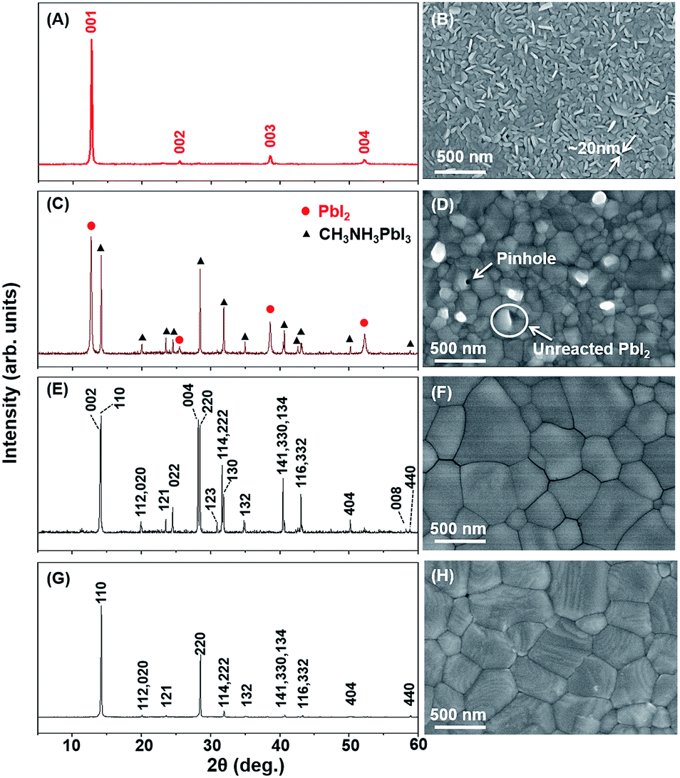 | ||
| Fig. 2 Indexed XRD patterns and corresponding SEM images (top surface) of films at the different stages during SVD growth: (A and B) after PbI2 vapour deposition; (C and D) partially reacted with MAI vapour (5 min); (E and F) fully reacted with MAI vapour (15 min); (G and H) after annealing at 100 °C for 30 min. | ||
It appears that the nanoporous nature of the vapour-deposited PbI2 film (Fig. 2B), with its large specific surface area, allows easy ingress and contact with MAI vapour, promoting rapid and more uniform reaction between PbI2 and MAI. This results in phase-pure MAPbI3 films that are pinhole-free, uniform, and smooth (Fig. 2F). Since the film thickness is ∼350 nm, and the size of the MAPbI3 grains is ∼500 nm, most of the MAPbI3 grains span the entire thickness of the film. In other words, majority of the grain boundaries in the SVD-processed MAPbI3 films are expected to run vertically between the substrate and the film surface, and that the horizontal grain boundaries across the path of carriers transport are likely to be in the minority.
Fig. 3A shows the UV-vis absorbance spectrum of the MAPbI3 perovskite film (on ITO) prepared by the SVD method and the corresponding differential transmission (ΔT/T) spectrum (inset is an optical photograph showing dark-colored film). The CH3NH3PbI3 perovskite film exhibits strong adsorption of UV-vis light up to ∼790 nm wavelength, which is consistent with what is reported in the literature.8,14,15 However, from the differential transmission spectrum, the SVD-processed CH3NH3PbI3 perovskite film shows only one intense photobleaching peak at ∼760 nm which is assigned to the direct band gap transition. The broad photobleaching peak at ∼480 nm, which is typically observed in MAPbI3 perovskite films, is virtually absent in the ΔT/T spectrum in Fig. 3A. This is probably related to unique band structure in the SVD-processed MAPbI3 perovskite films that exhibits unique crystal morphology. These distinct UV-vis absorption characteristics of the SVD-processed MAPbI3 perovskite films also indicate the likelihood of an efficient photo-induced charge transfer during the solar cell operation.16
 | ||
| Fig. 3 (A) UV-vis absorption spectrum and transformed differential transmission spectrum of MAPbI3 perovskite film (inset: optical photograph). (B) Cross-sectional SEM image of a MAPbI3/C60 solar cell (false color). (C) Current density (J) – voltage (V) response of a MAPbI3/C60 solar cell under AM1.5G one sun illumination (top inset: energy-levels diagram; bottom inset: extracted solar cell performance parameters). | ||
Fig. 3B is a color-enhanced cross-sectional SEM image of a typical MAPbI3/C60 bilayer solar cell fabricated in this study, illustrating the simple cell architecture. All three layers—MAPbI3, C60, Ag—are vapour deposited (see ESI†). The energy-levels diagram of this simple cell architecture is shown in the Fig. 3C inset. Here the MAPbI3 film serves as absorber, electron-donor, hole-conductor, and electron-blocking layer. Whereas the C60 layer serves as electron-acceptor, electron-conductor, and hole-blocking layer. Since MAPbI3 is a good hole-conductor, additional hole-conducting layers typically used in perovskite-based solar cells can be eliminated while retaining high PCEs.17–19 Furthermore, the widely used mesoporous TiO2 electron-acceptor/-conductor scaffold and/or dense TiO2 hole-blocking layer, which require high-temperature processing, have been eliminated in these solar cells.17–19 Efficient electron-hole dissociation occurs at the MAPbI3/C60 interface, making C60 a promising candidate as a non-oxide electron-acceptor/-conductor and hole-blocking layer in perovskite-based solar cells.14,15
Fig. 3C shows a typical current density (J) – voltage (V) response of the MAPbI3/C60 bilayer solar cell under AM1.5G simulated one sun illumination, and the solar-cell performance parameters are reported in the inset. Ten solar cells were tested, and their performance data are summarized in Table S1 (see ESI†), with the PCE ranging from 4.1% to 5.4%. Considering the simplicity of these solar cells, a maximum PCE of 5.4%, an open-circuit voltage (VOC) of 0.8 V, and a short circuit current density (JSC) of 13.6 mA cm−2, are promising, and they can be attributed to the high quality of the SVD-processed MAPbI3 films. The estimate of the maximum VOC is given by:14
 | (1) |
Substituting the values from the energy-levels diagram in Fig. 3C (inset) in eqn (1), the maximum VOC is estimated at 1.0 V for the MAPbI3/C60 heterojunction, representing a 20% loss in the measured VOC (0.8 V) in the MAPbI3/C60 bi-layer solar cell (Fig. 3C).
Jeng et al.14 and Chiang et al.20 report PCEs of 1.6% and 3.62%, respectively, for solution-processed MAPbI3/C60 solar cells, but their solar cells also contain additional layers of poly(3,4-ehylenedioxythiophene) poly(styrene-sulfonated) (PEDOT:PSS) and bathocuproine (BCP). The PEDOT:PSS layer is the hole transporter and it appears necessary for one-step solution processing of MAPbI3,18 and the BCP layer is used as a hole-blocker. The voltage loss in MAPbI3/C60 solar cells by Jeng et al.17 is 45%, whereas cells by Chiang et al.10 show a lower loss of 16%. The use of a layer of a C60 derivate—(6,6)-phenyl-C61-butyric acid methyl ester (PC61BM)—instead of the C60 layer, in solution-processed MAPbI3/PC61BM solar cells results in higher PCE (7.4%),18 however, those cells also use the additional layer of PEDOT:PSS. The maximum estimated VOC for these MAPbI3/PC61BM is 1.23 V, and the measured VOC in those cells is 0.91 V (ref. 18) or a 26% loss. Thus, the voltage loss in the simple MAPbI3/C60 bi-layer solar reported here is one of the lowest for solar cells based on MAPbI3/fullerene heterojunctions, which is attributed to the improved coverage of perovskite film by SVD method.
With regard to JSC, the measured value of 13.6 mA cm−2 reported here is the highest among all the MAPbI3/fullerene heterojunction solar cells reported so far.14,15,20 This is attributed to the relatively thicker and denser SVD-processed MAPbI3 films used here that are able to absorb light more efficiently. The fill factor (FF) of 50% is relatively low in these MAPbI3/C60 solar cells, which could be due to various factors, including non-ideal electrical contacts. Thus, there is plenty of room for improvement in this regard through further optimization of the ITO surface and the C60/Ag interface.
Conclusions
An SVD method is demonstrated for the growth of high-quality MAPbI3 films, and the possible growth mechanisms are elucidated. This constitutes a new contribution to the menu of processing methods available for the growth of MAPbI3 perovskite films. The resulting MAPbI3 films are pinhole-free, uniform and smooth, and most of the textured MAPbI3 grains within the films span the entire thickness of the film. The high quality of the MAPbI3 films allowed us to fabricate hole-conductor-free planar MAPbI3 perovskite solar cells at low temperature (100 °C maximum) that deliver a promising PCE of 5.4% with VOC of 0.8 V. While the simple bi-layer cell architecture is used here to demonstrate the efficacy of the SVD process, high-quality MAPbI3 films grown by the SVD process can be used in more complex solar cell architectures for much higher performance, and also in other future optoelectronic devices.Acknowledgements
This research was funded by the Chinese National Natural Science Foundation (grant no. 51202266), Natural Science Foundation of Shandong Province (ZR2013FZ001), the Research Program of Qingdao (13-1-4-228-jch, 12-1-4-9-(4)-jch, 12-4-1-24-gx) and the U.S. National Science Foundation (grant no. DMR-1305913).Notes and references
- G. Hodes, Science, 2013, 342, 317–318 CrossRef CAS PubMed.
- B. V. Lotsch, Angew. Chem., Int. Ed., 2014, 53, 635–637 CrossRef CAS PubMed.
- S. Kazim, M. K. Nazeeruddin, M. Grätzel and S. Ahmad, Angew. Chem., Int. Ed., 2014, 53, 2812–2824 CrossRef CAS PubMed.
- J. Burschka, N. Pellet, S. J. Moon, R. Humphry-Baker, P. Gao, M. K. Nazeeruddin and M. Gratzel, Nature, 2013, 499, 316–319 CrossRef CAS PubMed.
- N. G. Park, J. Phys. Chem. Lett., 2013, 4, 2423–2429 CrossRef CAS.
- H. S. Kim, S. H. Im and N. G. Park, J. Phys. Chem. C, 2014, 118, 5615–5625 CAS.
- A. Kojima, K. Teshima, Y. Shirai and T. Miyasaka, J. Am. Chem. Soc., 2009, 131, 6050–6051 CrossRef CAS PubMed.
- G. C. Xing, N. Mathews, S. Y. Sun, S. S. Lim, Y. M. Lam, M. Grätzel, S. Mhaisalkar and T. C. Sum, Science, 2013, 342, 344–347 CrossRef CAS PubMed.
- O. Malinkiewicz, A. Yella, Y. H. Lee, G. M. Espallargas, M. Grätzel, M. K. Nazeeruddin and H. J. Bolink, Nat. Photonics, 2014, 8, 128–132 CrossRef CAS.
- Q. Chen, H. Zhou, Z. Hong, S. Luo, H. S. Duan, H. H. Wang, Y. Liu, G. Li and Y. Yang, J. Am. Chem. Soc., 2014, 136, 622–625 CrossRef CAS PubMed.
- M. Liu, M. B. Johnston and H. J. Snaith, Nature, 2013, 501, 395–398 CrossRef CAS PubMed.
- J. M. Ball, M. M. Lee, A. Hey and H. J. Snaith, Energy Environ. Sci., 2013, 6, 1739–1743 CAS.
- E. Edri, S. Kirmayer, A. Henning, S. Mukhopadhyay, K. Gartsman, Y. Rosenwaks, G. Hodes and D. Cahen, Nano Lett., 2014, 14, 1000–1004 CrossRef CAS PubMed.
- S. Y. Sun, T. Salim, N. Mathews, M. Duchamp, C. Boothroyd, G. C. Xing, T. C. Sum and Y. M. Lam, Energy Environ. Sci., 2014, 7, 399–407 CAS.
- J. Y. Jeng, Y. F. Chiang, M. H. Lee, S. R. Peng, T. F. Guo, P. Chen and T. C. Wen, Adv. Mater., 2013, 25, 3727–3732 CrossRef CAS PubMed.
- A. Marchioro, J. Teuscher, D. Friedrich, M. Kunst, R. Krol, T. Moehl, M. Grätzel and J. E. Moser, Nat. Photonics, 2014, 8, 250–255 CrossRef CAS.
- L. Etgar, P. Gao, Z. S. Xue, Q. Peng, A. K. Chandiran, B. Liu, M. K. Nazeeruddin and M. Grätzel, J. Am. Chem. Soc., 2012, 134, 17396–17399 CrossRef CAS PubMed.
- W. Abu Laban and L. Etgar, Energy Environ. Sci., 2013, 6, 3249–3253 Search PubMed.
- J. Shi, J. Dong, S. Lv, Y. Xu, L. Zhu, J. Xiao, X. Xu, H. Wu, D. Li, Y. Luo and Q. Meng, Appl. Phys. Lett., 2014, 104, 063901 CrossRef PubMed.
- Y. F. Chiang, J. Y. Jeng, M. H. Lee, S. R. Peng, P. Chen, T. F. Guo, T. C. Wen, Y. J. Hsu and C. M. Hsu, Phys. Chem. Chem. Phys., 2014, 16, 6033–6040 RSC.
Footnote |
| † Electronic supplementary information (ESI) available. See DOI: 10.1039/c4ra03820g |
| This journal is © The Royal Society of Chemistry 2014 |