
 Open Access Article
 This Open Access Article is licensed under a
 Creative Commons Attribution 3.0 Unported Licence
Origin and effect of In–Sn ordering in InSnCo3S2: a neutron diffraction and DFT study†
Jan
Rothballer
a,
Frederik
Bachhuber
ab,
Stefan M.
Rommel
a,
Tilo
Söhnel
*bc and
Richard
Weihrich
*a
aUniversität Regensburg, Institute of Inorganic Chemistry, Universitätsstraße 31, 93040 Regensburg, Germany. E-mail: richard.weihrich@ur.de; Web: http://www.uni-regensburg.de/chemie-pharmazie/anorganische-chemie-weihrich/ Fax: +49-941-943-4983
bSchool of Chemical Sciences, The University of Auckland, Private Bag, 92019, Auckland, New Zealand. E-mail: t.soehnel@auckland.ac.nz; Web: http://www.science.auckland.ac.nz/people/t-soehnel
cCentre for Theoretical Chemistry and Physics, The New Zealand Institute for Advanced Study, Massey University, Auckland, New Zealand
First published on 29th August 2014
Abstract
The solid solution In2−xSnxCo3S2 is attractive due to a variety of interesting properties depending on the In/Sn content, i.e. half metal ferromagnetic Sn2Co3S2, low dimensional metal In2Co3S2, and semiconducting thermoelectric InSnCo3S2. For the latter, crystal structure effects and a metal to insulator transition are not only related to electron counting but also to ordering of In and Sn within and between Co Kagomé nets. These observations have not been adequately understood to date. The degree of ordering is now evaluated from neutron diffraction data to distinguish In and Sn. The origin and effects on crystal and electronic structures are studied by DFT calculations on a superstructure model. Relations of local bonding (electron localization function ELF and Bader's AIM theory), In/Sn site preference, crystal structure distortions, and the opening of the gap are explored. Results are generalised from predictions on isoelectronic compounds.
Introduction
Structure–property relations are the backbone of research on modern materials. Therein, low dimensional structures help to design storage, superconducting, magnetic and thermoelectric properties, and topological insulators.1–3 As a second adjusting screw, electronic flexibility is exploited. A promising combination of structural and electronic properties is given for thiocobaltates A2[Co3Ch2] (A = Sn, In; Ch = S, Se).4 Within the solid solution In2−xSnxCo3S2, the half metal ferromagnet (HFM) Sn2Co3S2,5 the low dimensional metal In2Co3S2,6 and low gap semiconducting thermoelectric InSnCo3S27,8 were discovered. These compounds consist of layered partial structures [Co3S2]δ−. Their trigonal shandite (Pb2Ni3S2) type crystal structures are understood by the concept of ordered half antiperovskites (HAP).4,9 It deduces the crystal structures from antiperovskites like MgNi3C10 as Co atoms occupy half of the available S2A4 sites therein, similar to superconducting parkerites (Bi2Ni3S2).9The behaviour of the mentioned A2Co3S2 compounds is ostensibly understood by electron counting. For InSnCo3S2 (46 valence electrons, VE), the Fermi energy (EF) is found in a band gap. For the pure A = In (45 VE) and Sn (47 VE) compounds, it is shifted above or below EF and causes metal and magnetic properties. However, in case of InSnCo3S2 the semiconducting properties were not only found to be sensitive to electron counting. Due to DFT calculations ordering of In and Sn on crystallographic sites between and within the Co Kagomé lattices opens and closes the gap.11 A completely ordered semiconducting ground state is predicted to be preferred in energy by 0.11 eV with respect to the ordered metallic state. This prediction is in line with the observation of semiconducting and thermoelectrical properties.7,8 However, non-Vegard like behaviour of crystal structure data, trigonal distortion in the solid solution In2−xSn2Co3S2, and 119Sn-Mößbauer spectroscopy on powder samples indicate incomplete ordering and site preference for In and Sn.11 These observations are not yet understood and raise the question on the real structure and origin and effects of partial In/Sn disorder on electronic and crystal structure in InSnCo3S2. If a general principle applies, substitution effects should allow for a systematic design of novel exciting HAP compounds.
As In and Sn cannot be distinguished by X-rays, high resolution neutron powder diffraction measurements were performed as the method of choice on the ECHIDNA instrument at the OPAL reactor12 on In2Co3S2, InSnCo3S2, and Sn2Co3S2. From refined diffraction data a supercell model was obtained for DFT modelling. The origin of crystal and electronic structure effects on bonding of In and Sn were analysed in direct space using the Electron Localization Function (ELF)13 and Bader's theory of atoms in molecules (AIM).14 Special attention is spent on the question of multicenter metal bonds as found for Laves phases.15 Finally, effects on crystal structures and band gaps upon substitution are probed by DFT modelling to conclude on general rules for novel promising materials.
Experimental and calculation methods
All In2−xSnxCo3S2 (x = 2, 1, 0) samples were prepared by high temperature solid state synthesis as described earlier.4–7 Neutron powder diffraction data was collected on the high resolution powder diffractometer ECHIDNA12 at the OPAL facility (Lucas Height, Australia), using neutrons with a wavelength of 1.62209 Å. For these measurements, the samples were contained in a 9 mm diameter vanadium can. Refinement of the neutron powder data was done with the Rietveld method within the FullProf suite program16 by using pseudo-Voigt functions for reflection profiles. The background was modelled by a polynom of 6th order. The zero point was refined. All quantum chemical calculations were performed with DFT-GGA methods.17 Full geometry optimizations were performed with a projector-augmented-wave (PAW) approach and the conjugant gradient algorithm as implemented in VASP4.6.18,19 Convergence is considered at differences in total energy less than 10−5 eV and maximum Hellmann–Feynman forces of 10−4 eV Å−1 as also applied earlier.20 DOS and band structures were executed with the scalar relativistic full-potential local orbital scheme (FPLO14).21 The calculations were converged to 12 × 12 × 12 k-point meshes (4 × 4 × 4 for supercells). For ELF and AIM analyses TOPOND98 and CRYSTAL9822 were used. Valence and all electron basis sets (In/Sn-976631d311G*, Co-86411d311G*, S-86311d1G*, see also ESI† and ref. 4 and 11) were optimised and tested for comparable performance in crystal and electronic structure prediction with CRYSTAL09.22Results and discussion
Neutron powder diffraction
Measured neutron powder diffraction patterns for In2Co3S2, InSnCo3S2, and Sn2Co3S2 (Fig. 1) were refined first within the shandite-type structure (space group R![[3 with combining macron]](https://www.rsc.org/images/entities/char_0033_0304.gif) m) as found from earlier investigations.4,23 The trigonal distortion from the A = Sn to the A = In containing compounds is seen from a splitting of prominent reflections. Sn2Co3S2 is metrically cubic (a = 5.36 Å, c = 13.16 Å, Table 1). The values found for InSnCo3S2 (5.31 Å, 13.47 Å) are closer to In2Co3S2 (5.31 Å, 13.65 Å).23 Shorter ahex, longer chex axes, i.e. larger c/a values signal non-Vegard behaviour as found in the solid solution In2−xSnxCo3S2.4,7,8 Therein, A = In, Sn atoms form a primitive substructure (Fig. 2). It splits to 3a (0,0,0) and 3b (0,0,1/2) sites, subsequently named A1 and A2 with respect to positions between (3a) and within (3b) Kagomé nets of Co atoms on 9d (0,1/2,1/2).11 Sulphur atoms on 6c (0,0,z) centre the A substructure and form [Co3S2] networks with linear, short S–Co–S bonds (dCo–S < 2.2 Å).6 In InSnCo3S2 the A site occupation offers three possibilities (see Table 2): all indium atoms on A1 and all tin atoms on A2 sites (scheme SI), opposite (SV), or mixed occupation of both sites (SIII) by In and Sn. According to R values from present Rietveld refinements, SI is preferred over SV. In scheme III the occupation numbers of In and Sn were coupled to sum up to one for each position 3a and 3b. The obtained preference of 69% for Sn on 3b and In on 3a agrees with the results from Mössbauer spectroscopy (70–80%).11
m) as found from earlier investigations.4,23 The trigonal distortion from the A = Sn to the A = In containing compounds is seen from a splitting of prominent reflections. Sn2Co3S2 is metrically cubic (a = 5.36 Å, c = 13.16 Å, Table 1). The values found for InSnCo3S2 (5.31 Å, 13.47 Å) are closer to In2Co3S2 (5.31 Å, 13.65 Å).23 Shorter ahex, longer chex axes, i.e. larger c/a values signal non-Vegard behaviour as found in the solid solution In2−xSnxCo3S2.4,7,8 Therein, A = In, Sn atoms form a primitive substructure (Fig. 2). It splits to 3a (0,0,0) and 3b (0,0,1/2) sites, subsequently named A1 and A2 with respect to positions between (3a) and within (3b) Kagomé nets of Co atoms on 9d (0,1/2,1/2).11 Sulphur atoms on 6c (0,0,z) centre the A substructure and form [Co3S2] networks with linear, short S–Co–S bonds (dCo–S < 2.2 Å).6 In InSnCo3S2 the A site occupation offers three possibilities (see Table 2): all indium atoms on A1 and all tin atoms on A2 sites (scheme SI), opposite (SV), or mixed occupation of both sites (SIII) by In and Sn. According to R values from present Rietveld refinements, SI is preferred over SV. In scheme III the occupation numbers of In and Sn were coupled to sum up to one for each position 3a and 3b. The obtained preference of 69% for Sn on 3b and In on 3a agrees with the results from Mössbauer spectroscopy (70–80%).11
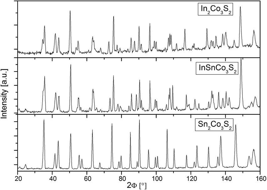 | ||
| Fig. 1 Neutron powder diffraction patterns of In2−xSnxCo3S2 (x = 2, 1, 0). | ||
| In2Co3S2 | InSnCo3S2 | Sn2Co3S2 | |
|---|---|---|---|
| Diffractometer | Echidna | ||
| Temperature [K] | 298 | 298 | 298 |
| Space group |
Rm |
Rm |
Rm |
| a hex [Å] | 5.3129(7) | 5.3124(6) | 5.3638(4) |
| c hex [Å] | 13.652(2) | 13.478(2) | 13.166(1) |
| a sup [Å] | 7.6384(8) | 7.6035(5) | 7.5909(3) |
| α sup [°] | 88.143(1) | 88.642(1) | 89.919(1) |
| Z(S) | 0.2791(3) | 0.2808(3) | 0.2818(2) |
| B iso Co on 9d [Å2] | 0.68(5) | 0.51(4) | 0.49(5) |
| B iso In/Sn on 3a [Å2] | 1.59(8) | 0.90(9) | 0.70(7) |
| B iso In/Sn on 3b [Å2] | 1.36(9) | 0.65(8) | 0.26(6) |
| B iso S on 6c [Å2] | 0.77(7) | 0.77(6) | 0.37(7) |
| ρ calc [g cm−3] | 7.017 | 7.175 | 7.261 |
| V [Å]3 | 333.72(9) | 329.42(7) | 328.06(4) |
| R p | 3.70 | 3.65 | 3.40 |
| R wp | 4.83 | 4.90 | 4.62 |
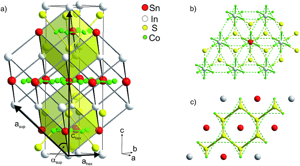 | ||
| Fig. 2 (a) Hexagonal crystallographic cell (ahex, chex) and primitive supercell (asup, αsup), (b) occupation of 75% of A1 sites by In, (c) of 75% A2 sites by Sn. | ||
| Occupation scheme | SI | SII | SIII | SIV | SV |
|---|---|---|---|---|---|
| In on 3a [%] | 100 | 75 | 69(4) | 25 | 0 |
| In on 3b [%] | 0 | 25 | 31(4) | 75 | 100 |
| R p | 3.78 | 3.67 | 3.67 | 3.88 | 4.15 |
| R wp | 5.08 | 4.94 | 4.93 | 5.20 | 5.68 |
Mixed occupation of In and Sn on inter-A1 and intralayer A2 sites in InSnCo3S2 is modelled within a trigonal supercell (Fig. 2a–c). It is obtained by a klassengleiche supergroup-relation from the crystallographic cell by doubling the ahex axis (ahsup = 2 × ahex).6 The related primitive cell pictures the 8-fold perovskite-related superstructure of the HAP concept4,9 as deduced from antiperovskites like MgNi3C.11,24 The trigonal distortion therein is reflected by the deviation of the supercell angle αsup = 90° for Sn2Co3S2 to 88° for In2Co3S2. The primitive A site substructure is now split into two A1 sites, i.e. 1a (0,0,0) and 3d (0,0,1/2), and two A2 sites, i.e. 1b (1/2,1/2,1/2) and 3e (1/2,0,1/2). In the hexagonal setting A1 sites are 3a and 9e (1/2,0,0), and A2 sites 3b and 9e (1/2,0,1/2). The occupation of A1 and A2 sites by In and Sn is modelled similar to partial substitution in the solid solution In2−xSnxCo3S2 (x = 1/4, 3/4, 1¼, 1¾).6 However, here we focus on the effect of A site occupation for the InSnCo3S2 composition. According to the refinements a scheme with 75% Sn on A2 and 75% In on A1 sites (SII, Fig. 2b and c) serves as an appropriate model with R values close to the SIII scheme, while the opposite occupation (SIV) is less preferred.
DFT calculations
Electronic effects of A site occupation were thus computed with respect to the SI, SII, SIV, and SV schemes after full structure optimisations (Fig. 3). It helps to gain a better insight into the semiconductor to metal transition of InSnCo3S2. The gap remains when 25% of A2 sites are occupied by In and A1 sites by In. Thus, not only complete ordering with In on A1 sites and Sn on A2 sites results in semiconducting behaviour. This is in line with the experimentally found semiconducting and thermoelectric properties. To the contrary, metal behaviour is predicted to occur already for scheme SIV when 75% of A2 sites within the Co layers are occupied by In and 75% of A1 sites by Sn. At this point one might conclude on a continuous transition from semiconducting to metal characteristics between schemes SII and SIV that might be interesting for e.g. topological insulators that are related to thermoelectrics.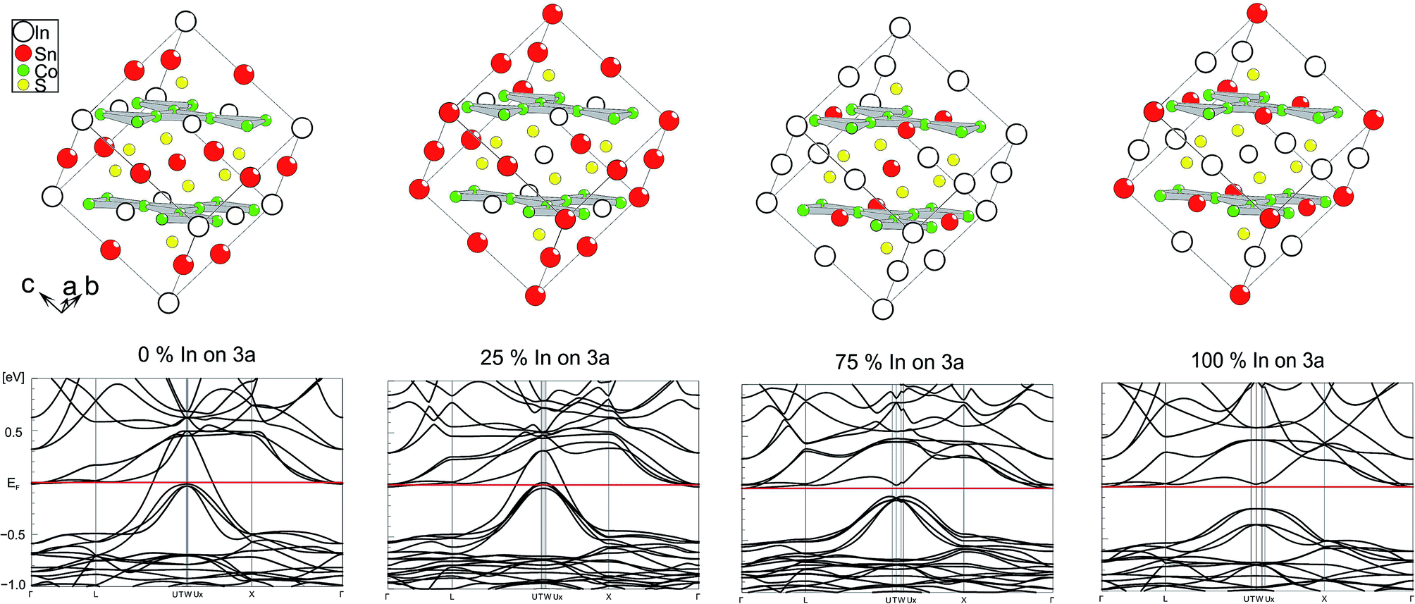 | ||
| Fig. 3 Electronic band structure for different supercell occupation schemes (SV, SIV–SII, SI from left to right). | ||
One can conclude now on the relation of A site occupation and the closing of the gap looking again at the electronic structures of Sn2Co3S2, InSnCo3S2, and In2Co3S2 (Fig. 4). At first sight, semiconducting behaviour of InSnCo3S2 (46 VE) is only the result of Fermi level shifting. In Sn2Co3S2 (47 VE, type IA HFM) one electron per formula unit is found in a conduction band like state which is completely spin polarized in the electronic ground state. The resulting characteristics of a semiconductor for one spin channel and a metal for the second is interesting for spintronics.25
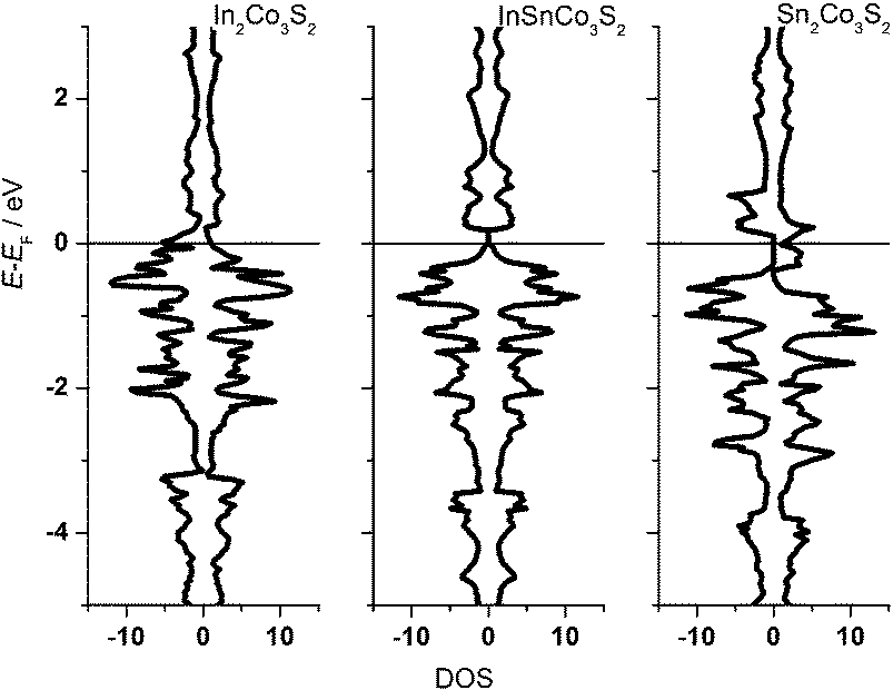 | ||
| Fig. 4 DOS for In2Co3S2 (45 electrons), InSnCo3S2 (46 electrons) and Sn2Co3S2 (47 electrons). | ||
InSnCo3S2 has one electron less. The Fermi energy (EF) is shifted into the gap for both spin channels. This is only true for preferred occupation of In on A1 sites. On A2 sites they cause metallic behaviour as previously seen. Accordingly, for In2Co3S2 not only a shift of EF below the gap is observed, but also a closing of the gap due to an electronic structure distortion. This was not understood from partial substitution of Sn by In.6 With the new results, one must conclude that the gap is not closed when In partially occupies A2 sites and Sn the A1 sites. As a content of 75% Sn on A2 sites keeps the gap open it seems mandatory that continuous Sn–Co–Sn–Co chains are maintained within the Co layers.
Next, the relations of A site occupation and crystal structure distortions are addressed by comparison of experimental data4,8 for In2Co3S2, InSnCo3S2, and Sn2Co3S2 with DFT predictions for ordered schemes of InSnCo3S2. According to the results (Fig. 5, see also ESI†) the asup and chex lattice parameters are continuous functions of In/Sn ordering on A1 and A2 sites that explain the kink of the curves.4,8 The experimental parameters deviate from values predicted for the fully ordered semiconducting SI scheme, but they are close to the results for the SII model. Towards the SIV and SV schemes calculated lattice parameters are closer to values known for Sn2Co3S2. Thus, replacing Sn by In causes huge changes in chex and ahex on the A1 site, but only minor effects on the A2 site. Similarly, a large contraction of chex and an enlargement of ahex are found, when In1 in In2Co3S2 is replaced by Sn. When all A2 sites in InSnCo3S2 are occupied by Sn, a contraction of the ahex axis is predicted (S1). Predicted structures are thus similar to In2Co3S2 for A1 = In, but similar to Sn2Co3S2 for A1 = Sn. One must conclude that the trigonal distortion is mainly driven by the A1 site. A1 = In causes longer chex and shorter ahex axis, A1 = Sn the contrary. A hint on the responsible bonds is given as ahex = 2dA2–Co = 2dCo–Co determines metal distances within the Kagomé layers, while the chex axis mainly affects the interlayer metal distances dA1–Co.
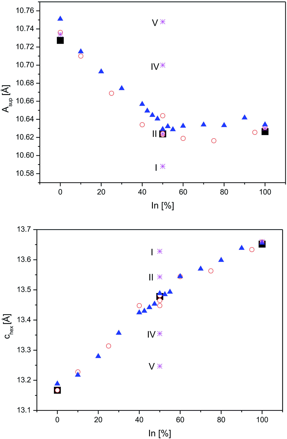 | ||
| Fig. 5 Lattice parameters from neutron data (square symbols) and DFT optimizations (stars) for InSnCo3S2 (SI, SII, SIV, and SV), compared to earlier XRD data from23 (triangles) and8 (circles) for In2−xSnxCo3S2 are shown for the asup (top) and the chex axes (below). | ||
Bonding analysis by ELF and AIM
Local bonds are analysed with respect to A = In, Sn site preference in InSnCo3S2 from the electron localization function (ELF)13 in Fig. 6a. The cut along the (200) plane is exemplified for the charge density of the cell (middle). It includes S, A1, and A2 sites perpendicular to the Co Kagomé layers. The same slide is applied for ELF analyses for occupation schemes I (left) and V (right). In both cases, ELF maxima around In and Sn indicate highly anisotropic valence charge distribution as signalled by quadrupole splitting from Mössbauer spectroscopy and calculated EFG values.11 This is in contrast to spherical 5s lone pairs as expected for ionic In(+I) and Sn(+II) (5s25p0). It is in line with bonding contributions of A-5s orbitals as concluded from 119Sn-Mössbauer isomer shifts (2.2 mm s−1). According to the ELF plots anisotropy in bonding of the A site atoms must be attributed to hybrid states from mixing of 5s and 5p. For both A positions, the valence charges of In and Sn point to Co neighbours and avoid the S neighbours. One can conclude on anisodesmic bonding26 for In and Sn that behave as donors for bonds to Co, but as acceptors for bonds to S neighbours.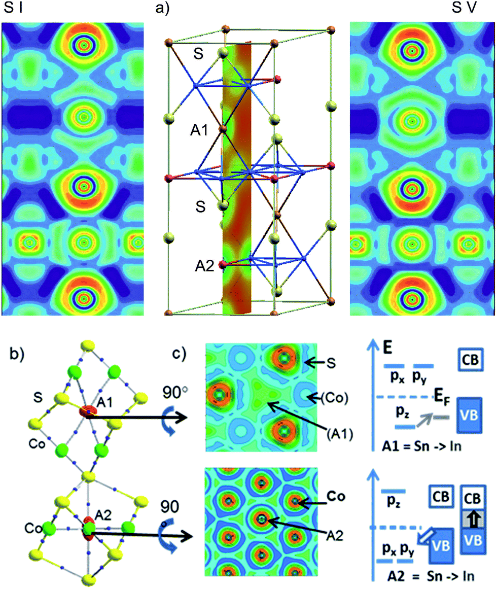 | ||
| Fig. 6 (a) Representation of the ELF for both occupation schemes: In between (A1) and Sn within (A2) the Co Kagomé layers (left) and vice versa (right). A part of the hexagonal unit cell is displayed in the centre including a cut through the (200) plane showing the charge density. (b) AIM analysis of bond critical points (black dots) and ELF slides perpendicular to chex below A1 and A2 and (c) orbital splitting of In/Sn-5pxy and 5pz orbitals for A1 and A2 sites. | ||
Metal A–Co bonds appear thus significant in InSnCo3S2 similar to Laves phases.15 Further, ionic A–S interactions must be considered to explain the found results. ELF valence maxima in Fig. 6 appear overloaded for Sn on A1 sites that interlink two Co3A1 tetrahedra. Within the Kagomé nets weak ELF maxima towards the Co neighbours indicate a deficit in valence electron density on A2 sites. Sn seems to have more than enough electrons for bonds on A1 sites, but In only few electrons to form bonds within the Kagomé layers.
The nature of the metal bonds is uncovered by ELF plots perpendicular to the chex axis at approx. 0.1 Å above the atomic positions of A1 and A2 (Fig. 6b, middle). They signal two 4-centre bonds to Co triangles above and below the A1 sites and six 3-centre bonds for A2 to Co neighbours within the Kagomé nets. Similar characteristics were found for Laves phases.15 Accordingly, the Co–A bonds determine crystal and electronic structure properties, as well as site preference in the shandites. On A1 sites In or Sn atoms form two sp-like hybrid orbitals and 4-centre bonds of corner shared tetrahedrons. The A1-5pz orbitals contribute to bonding here. The 5px, 5py-orbitals that point towards S neighbours are shift above EF. On A2 sites, the degenerate 5px and 5py orbitals contribute to bonding within the Kagomé nets. They are lowered in energy while 5pz is shifted above EF. The contrary behaviour of A1- and A2-5p orbitals is visualised by the crystal field like scheme in Fig. 6c. Now, the shortened chex and ahex axis are easily explained by stronger Sn–Co bonds compared to In–Co. This causes shorter chex axis for A1 = Sn and shorter ahex axis for A2 = Sn in InSnCo3S2. Concerning the band gap two effects turn out as significant: Sn has a higher core charge (50) and more valence electrons (4) than In (49, 3). The Sn-5s and 5p orbitals are lowered by 1 eV in shandites compared to A = In.11 On the A1 sites In has enough electrons for bonding with its 5pz orbital. The gap remains, when Sn is replaced by In here. On A2 sites, the degenerate In-5px,y-orbitals seemingly act as a sink for the valence band (VB). The gap to the conduction band (CB) closes. Here, the Sn-5px,y orbitals open the gap. This bonding situation is seen as the reason the for the incomplete preference site. Both, In and Sn can do the bonds on A1 and A2, but the latter is better done by Sn.
This picture is completed by an analyses according to the AIM (atoms in molecules) theory.14 In Fig. 6b (left) bond critical points (BCP) are drawn out. BCP are saddle points, i.e. (3, −1) critical points in the 3D charge density. Within the AIM theory, they indicate atomic interactions along a bond path (BP) for 2 atoms.27 Independent from the occupation scheme applied for InSnCo3S2 BCP are found for A1–Co, A2–Co, and Co–S within occupied tetragonal bipyramides Co[S2A12A22] by numerical analysis. Additional BCP are detected for S–S interactions within the unoccupied bipyramides [S2A12A22] and the shortened A2–S distance due to the shift z(S) along chex. No BCP are found for direct Co–Co or S–A1 interactions.
Extending the analysis to three dimensions, the BCP are situated on faces of zero flux surfaces (ZFS). In Fig. 7 atomic ZFS as obtained for InSnCo3S2 are related to the respective atomic coordination spheres. ZFS determine the surfaces of space filling atomic volumes. Integration of charge density therein reveals atomic volumes (Vat) and atomic charges (Qat). For the Co atoms the close S (dCo–S = 2.18 Å) and A neighbours determine the obtained tetragonally shaped ZFS. Its asymmetry is determined by distances dCo–A2 = ahex/2 and dCo–A1 = arh/2 that depend on the c/a ratio.
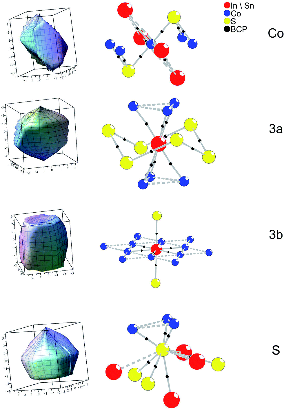 | ||
| Fig. 7 ZFS and atomic coordination with BCP (black dots) for InSnCo3S2. | ||
The ZFS of the A site atoms are clearly determined by bonding to the six Co neighbours. Additionally, the A2–S bonds (dSn2–S = 2.85 Å and dIn2–S) are mirrored by faces of the ZFS for A2 and S. For the S atoms, also three large faces point to the Co neighbours. Integrated atomic charges and volumes (Table 3) for In2Co3S2, Sn2Co3S2, and InSnCo3S2 clearly indicate a Co(0) state as expected from the linear S–Co–S coordination and the covalent [Co3S2] networks. Its atomic volume is comparable to metal Co. The charge of S (−0.6 to −0.7 e) is due to its covalent bonding to Co and ionic behaviour towards In and Sn. Concerning the A sites higher charges, but smaller atomic volumes are determined for the In than for the Sn atoms. Further, a certain disproportion between 3a (+0.75 to +0.83 e) and 3b (+0.67 to +0.70 e) sites is found for indium. In both occupation schemes (SI and SV) tin shows almost similar charges (+0.65 e to +0.69 e). The highest charge is found for In on 3a sites in the SI scheme, while it is lower in scheme SIV and In2Co3S2. Thus, the ordering in InSnCo3S2 is also related to charge balance.
| Q/e− | V/Å3 | ||
|---|---|---|---|
| Sn2Co3S2 | Sn(3a) | 0.638 | 19.49 |
| Sn(3b) | 0.646 | 19.00 | |
| Co | −0.026 | 11.71 | |
| S | −0.612 | 18.05 | |
| InSnCo3S2(SI) | In(3a) | 0.830 | 17.54 |
| Sn(3b) | 0.689 | 18.93 | |
| Co | −0.046 | 11.94 | |
| S | −0.686 | 18.68 | |
| InSnCo3S2(SV) | Sn(3a) | 0.672 | 19.78 |
| In(3b) | 0.767 | 17.47 | |
| Co | −0.033 | 12.18 | |
| S | −0.658 | 18.53 | |
| In2Co3S2 | In(3a) | 0.752 | 18.39 |
| In(3b) | 0.699 | 18.07 | |
| Co | −0.035 | 12.29 | |
| S | −0.670 | 16.06 |
Finally, a generalisation of structural and electronic characteristics found for InSnCo3S2 is concluded by modelling isoelectronic structures where either In or Sn in A1A2Co3S2 is substituted by A = Al, Ga, Tl, Si, Ge, Pb (Table 4). The results clearly show that in all cases semiconducting products are predicted when the main group III element is found on the A1 site and the main group IV element on the A2 site. The reduction of the cell volumes by 10% does not cause closing but larger band gaps for InSiCo3S2, InGeCo3S2, or InSnCo3O2. Inverse occupation closes the gap and causes systematically larger trigonal angles arh (and in turn large c/a values) as seen for PbInCo3S2 and SnTlCo3S2 similar to SnInCo3S2. Smaller band gaps are predicted for the substitution of In by Al and Ga, as well as for the substitution of S by Se. For InSnCo3Te2 a closing of the gap is predicted. These results confirm that the found behaviour of InSnCo3S2 can be generalized to isoelectonic shandites. Besides partial substitution of S by Se7 the mentioned compounds were not yet synthesised. However, the predicted data can give hints for the design of thermoelectric and related interesting properties of InSnCo3S2 based materials upon partial substitution.
| A1 | A2 | Ch | V/Å3 | a rh/Å | α/° | z(S) | ΔEgap/eV |
|---|---|---|---|---|---|---|---|
| In | Si | S | 100.8 | 5.423 | 55.4 | 0.282 | 0.329 |
| In | Ge | S | 103.9 | 5.442 | 56.2 | 0.281 | 0.300 |
| In | Sn | O | 99.3 | 5.262 | 58.4 | 0.259 | 0.291 |
| In | Sn | S | 110.2 | 5.472 | 57.9 | 0.280 | 0.206 |
| Sn | In | S | 111.0 | 5.405 | 59.7 | 0.228 | 0 |
| In | Pb | S | 114.4 | 5.522 | 58.3 | 0.277 | 0.187 |
| Pb | In | S | 114.7 | 5.519 | 58.5 | 0.276 | 0 |
| In | Sn | Se | 118.3 | 5.673 | 56.5 | 0.285 | 0.153 |
| In | Pb | Se | 122.5 | 5.706 | 57.1 | 0.283 | 0.151 |
| In | Pb | Te | 136.9 | 6.017 | 55.2 | 0.288 | 0 |
| Al | Sn | S | 103.1 | 5.285 | 59.5 | 0.283 | 0.077 |
| Ga | Sn | S | 104.1 | 5.281 | 60.0 | 0.283 | 0.066 |
| Tl | Sn | S | 113.4 | 5.529 | 57.8 | 0.277 | 0.197 |
| Sn | Tl | S | 114.2 | 5.478 | 59.2 | 0.276 | 0 |
| Tl | Sn | Se | 121.3 | 5.702 | 56.8 | 0.283 | 0.163 |
Conclusions
We investigated the effect of In and Sn ordering in InSnCo3S2 on electronic and crystallographic structure distortion. To clarify the percentage and the driving force for ordering of In and Sn, neutron powder diffraction measurements were applied and compared with detailed quantum chemical calculations based on DFT. The room temperature neutron powder diffraction data show a clear preference for In between the Co Kagomé layers, but a complete ordering cannot be observed at room temperature. To study the metal to insulator transition for partial ordering, a supercell was established. DFT structure predictions thereon show good agreement with crystallographic results, not for complete (100%), but for 75% a site preference of In on A1 and Sn on A2. The found model still shows semiconducting behaviour. It explains thus the experimentally found crystal structure, incomplete ordering, and the thermoelectric properties. Crystal and electronic structure effects could be related to local bonding of In and Sn from ELF and AIM analyses. Based on these investigations, anisotropic metal A1–Co and A2–Co bonds are identified as main reasons to cause site preference, crystal and electronic structure distortions. Modelling of crystal and electronic structures confirms similar effects upon isoelectronic substitution of InSnCo3S2 and gives hints to design systematically properties of related known and novel HAP compounds.Acknowledgements
We thank Maxim Adeev (ANSTO) for this help while performing experiments on Echinda beamline at ANSTO as well as Holger Kohlmann for the support with data refinement. The Deutsche Forschungsgemeinschaft (DFG, WE 4284/1-2) and the DAAD is acknowledged for financial support. We would like to thank and acknowledge the financial support provided by the Australian Institute of Nuclear Science and Engineering Inc. (AINSE).References
- S. M. Rommel, N. Schall, C. Brünig and R. Weihrich, Monatsh. Chem., 2014, 145, 385–404 CrossRef CAS PubMed.
- (a) M. Wuttig, D. Lusebrink, D. Wamwangi, W. Welnic, M. Gillessen and R. Dronskowski, Nat. Mater., 2007, 6, 122–U127 CrossRef CAS PubMed; (b) L. Müchler, F. Casper, B. Yan, S. Chadov and C. Felser, Phys. Status Solidi RRL, 2013, 7, 91–100 CrossRef.
- T. Nilges, O. Osters, M. Bawohl, J. L. Bobet, B. Chevalier, R. Decourt and R. Weihrich, Chem. Mater., 2010, 22, 2946–2954 CrossRef CAS.
- (a) R. Weihrich, I. Anusca and M. Zabel, Z. Anorg. Allg. Chem., 2005, 631, 1463–1470 CrossRef CAS; (b) R. Weihrich and I. Anusca, Z. Anorg. Allg. Chem., 2006, 632, 1531–1537 CrossRef CAS.
- W. Schnelle, A. Leithe-Jasper, H. Rosner, F. M. Schappacher, R. Poettgen, F. Pielnhofer and R. Weihrich, Phys. Rev. B 88, 2013, 205116 Search PubMed.
- F. Pielnhofer, J. Rothballer, P. Peter, W. Yan, F. M. Schappacher, R. Poettgen and R. Weihrich, Z. Anorg. Allg. Chem., 2014, 640, 286–294 CrossRef CAS.
- (a) A. Umetani, E. Nagoshi, T. Kubodera and M. Matoba, Phys. B, 2008, 403, 1356–1358 CrossRef CAS PubMed; (b) M. Fujioka, T. Sibuya, J. Nakai, K. Yoshiyasu, Y. Takano, Y. Kamihara and M. Matoba, arXiv preprint arXiv:1211.4467, 2012; (c) S. Natarajan, G. V. S. Rao, R. Baskaran and T. S. Radhakrishnan, J. Less-Common Met., 1988, 138, 215–224 CrossRef CAS.
- J. Corps, P. Vaqueiro and A. V. Powell, J. Mater. Chem. A, 2013, 6553–6557 CAS.
- (a) R. Weihrich, S. F. Matar, V. Eyert, F. Rau, M. Zabel, M. Andratschke, I. Anusca and T. Bernert, Prog. Solid State Chem., 2007, 35, 309–327 CrossRef CAS PubMed; (b) R. Weihrich, S. F. Matar, V. Eyert, I. Anusca, F. Bachhuber and S. Seidlmayer, J. Solid State Chem., 2011, 184, 797–804 CrossRef CAS PubMed.
- T. He, Q. Huang, A. P. Ramirez, Y. Wang, K. A. Regan, N. Rogado, M. A. Hayward, M. K. Haas, J. S. Slusky, K. Inumara, H. W. Zandbergen, N. P. Ong and R. J. Cava, Nature, 2001, 411, 54–56 CrossRef CAS PubMed.
- J. Rothballer, F. Bachhuber, F. Pielnhofer, F. M. Schappacher, R. Poettgen and R. Weihrich, Eur. J. Inorg. Chem., 2013, 248–255 CrossRef CAS.
- K.-D. Liss, B. Hunter, M. Hagen, T. Noakes and S. Kennedy, Phys. B, 2006, 385–386, 1010–1012 CrossRef CAS PubMed.
- A. D. Becke and K. E. Edgecombe, J. Chem. Phys., 1990, 92, 5397–5403 CrossRef CAS PubMed.
- R. F. Bader, Atoms in molecules, Oxford university press, 1990 Search PubMed.
- O. Osters, T. Nilges, M. Schoneich, P. Schmidt, J. Rothballer, F. Pielnhofer and R. Weihrich, Inorg. Chem., 2012, 51, 8119–8127 CrossRef CAS PubMed.
- J. Rodriguez-Carvajal and T. Roisnel, Mater. Sci. Forum, 2004, 443–4, 123–126 CrossRef.
- J. P. Perdew, K. Burke and M. Ernzerhof, Phys. Rev. Lett., 1996, 77, 3865–3868 CrossRef CAS.
- (a) G. Kresse and J. Hafner, Phys. Rev. B: Condens. Matter Mater. Phys., 1994, 64, 14251–14269 CrossRef; (b) G. Kresse and J. Furthmuller, Comput. Mater. Sci., 1996, 6, 15–50 CrossRef CAS; (c) G. Kresse and J. Furthmuller, Phys. Rev. B: Condens. Matter Mater. Phys., 1996, 54, 11169–11186 CrossRef CAS.
- G. Kresse and D. Joubert, Phys. Rev. B: Condens. Matter Mater. Phys., 1999, 59, 1758–1775 CrossRef CAS.
- (a) F. Bachhuber, J. Rothballer, T. Söhnel and R. Weihrich, J. Chem. Phys., 2013, 139, 214705 CrossRef CAS PubMed; (b) R. Weihrich, V. Eyert and S. F. Matar, Chem. Phys. Lett., 2003, 373, 636–641 CrossRef CAS; (c) R. Weihrich, S. F. Matar, E. Betranhandy and V. Eyert, Solid State Sci., 2003, 5, 701–704 CrossRef CAS.
- (a) H. E. K. Koepernik, Phys. Rev. B: Condens. Matter Mater. Phys., 1999, 59, 1743–1757 CrossRef; (b) K. K. I. Opahle and H. Eschrig, Phys. Rev. B: Condens. Matter Mater. Phys., 1999, 60, 14035–14041 CrossRef.
- (a) V. R. Saunders, R. Dovesi, C. Roetti, M. Causá, N. M. Harrison, R. Orlando and C. M. Zicovich-Wilson, CRYSTAL98, User's Manual, Universityof Torino, 1998 Search PubMed; (b) R. Dovesi, V. R. Saunders, C. Roetti, R. Orlando, C. M. Zicovich-Wilson, F. Pascale, B. Civalleri, K. Doll, N. M. Harrison, I. J. Bush, Ph. D'Arco and M. Llunell, CRYSTAL09, User's Manual, University of Torino, 2009 Search PubMed; (c) C. Gatti, Topond98, user's manual, Milano, 1998 Search PubMed.
- P. Vaqueiro and G. G. Sobany, Solid State Sci., 2009, 11, 513–518 CrossRef CAS PubMed.
- L. J. Huetter and H. H. Stadelmaier, Acta Metall., 1958, 6, 367–370 CrossRef CAS.
- C. Felser, G. H. Fecher and B. Balke, Angew. Chem., 2007, 119, 680–713 ( Angew. Chem., Int. Ed. , 2007 , 46 , 668–699 ) CrossRef.
- M. K. A. Baranov, F. R. Wagner, Y. Grin, R. Kniep and W. Bronger, Z. Anorg. Allg. Chem., 2008, 634, 2747–2753 CrossRef.
- R. F. W. Bader, W. H. Henneker and P. E. Cade, Chem. Phys., 1967, 46, 3341–3363 CAS.
Footnote |
| † Electronic supplementary information (ESI) available: Supplementary information is available on VASP and CRYSTAL optimisations and obtained structures. Deposited structure data includes atomic site parameters for the supercells. CCDC 933688, 933689 and 933690. For ESI and crystallographic data in CIF or other electronic format see DOI: 10.1039/c4ra03800b |
| This journal is © The Royal Society of Chemistry 2014 |