Structural properties and electrical characteristics of Ho2O3 and HoTixOy gate dielectrics for a-InGaZnO thin-film transistors

Tung-Ming Pan*, Ching-Hung Chen and Jiang-Hung Liu
Department of Electronics Engineering, Chang Gung University, Taoyuan 333, Taiwan. E-mail: tmpan@mail.cgu.edu.tw; Fax: +886-3-2118507; Tel: +886-3-2118800 ext. 3349

Received 18th April 2014 , Accepted 19th June 2014

First published on 19th June 2014


Abstract

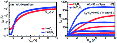
In this study, we developed high-κ Ho2O3 and HoTixOy gate dielectrics for amorphous indium–gallium–zinc oxide (a-IGZO) thin-film transistor (TFT) applications. X-ray diffraction, atomic force microscopy, and X-ray photoelectron spectroscopy were used to study the structural, morphological and chemical features of Ho2O3 and HoTixOy dielectric films. Compared with the Ho2O3 dielectric, the a-IGZO TFT incorporating the high-κ HoTixOy gate dielectric exhibited very good electrical characteristics, such as a high Ion/off ratio of 1.1 × 10⁸, a high field effect mobility of 20.6 cm2 V−1 s−1, a low threshold voltage of 0.23 V, and a low subthreshold swing of 183 mV decade−1. These results are probably due to the incorporation of Ti into the Ho2O3 film, resulting in the formation of a smooth surface and a low density of interface states at the oxide/channel interface. In addition, the stability of high-κ Ho2O3 and HoTixOy a-IGZO TFTs was investigated under positive gate-bias stress (PGBS) and negative gate-bias stress (NGBS). The electron charge trapping at the dielectric–channel interface resulted from the PGBS, whereas the oxygen vacancies occurred in the a-IGZO under the NGBS.


Introduction

Amorphous oxide semiconductors (AOSs) are actively researched for applications to transparent electronics, backplanes of large area active-matrix organic light-emitting diode displays, and liquid-crystal displays.1–3 Among various AOS materials, amorphous indium–gallium–zinc oxide (a-IGZO) is considered one of the most promising channel materials for thin-film transistors (TFTs) because of its high field effect mobility (μFE), low leakage current, good uniformity and stability, high transparency to visible light, and low process temperature.2–7 In order to obtain excellent device performance, a-IGZO materials with high carrier mobility are critical. Moreover, a high-capacitance gate dielectric is also desired to achieve a low operating voltage to reduce the device power consumption. Insulating silicon dioxide (SiO2) has been traditionally used as the gate dielectric material in IGZO TFTs. However, SiO2 with a moderate dielectric constant (3.9) is not an ideal material for high-capacitance gate dielectric. In addition, SiO2 thin-film easily induces higher leakage current due to direct tunnelling through the film,8 which makes it difficult to obtain high-performance IGZO TFTs. Therefore, search for stable and high-capacitance gate dielectric to replace SiO2 is currently one of the most important tasks and challenges in IGZO TFTs. High dielectric constant (high-κ) materials as a gate dielectric have been investigated to maintain the high capacitance density and inhibit the gate direct tunnelling current.9–12 In addition to the electrical requirements, such as a high dielectric constant, low gate current, low interface state density, and good thermal stability, are also very important for high-κ materials. IGZO TFTs featuring high-κ materials such as Al2O3, Ta2O5, or HfO2 were already reported in the literature.13–15 Given the physical deposition processes, interface quality is expected to be considerably worse than the one achieved with the conventional SiO2.12 Most of high-κ dielectrics present a polycrystalline structure and have a rough surface, leading to reduced reliability and degraded interface properties.8,16

To solve the problems related with high-κ dielectrics, thin rare-earth (RE) oxides have attracted interest for use as gate dielectrics for TFT applications because they have high dielectric constants and good thermal stability.17,18 Holmium oxide (Ho2O3) film has been studied for gate dielectric applications due to its high κ value, wide bandgap energy, high breakdown field, and low leakage current.19–22 Exposure to air, however, causes hygroscopic lanthanide oxides to react with moisture to form hydroxides,23 causing lower values of κ. The incorporation of Ti or TiO2 films into RE oxides increases their stability toward moisture.24 van Dover25 also demonstrated that the Ti adding RE oxide exhibited excellent electrical performance. Moreover, we reported that HoTiO3 thin-film as a gate dielectric showed excellent electrical characteristics such as a high capacitance value, a low density of interface state, a small leakage current, and almost no hysteresis voltage.26,27 Up to date, the physical and electrical properties of Ho2O3 and HoTixOy films as a gate dielectric for a-IGZO TFT devices are still not known. In addition, the reliability and stability are also key concerns for practical TFT applications, and the gate bias stress test is a general method that is used to determine the electrical stability of such an a-IGZO TFT device.28 In this paper, we compared the structural properties and electrical characteristics of high-κ Ho2O3 and HoTixOy gate dielectrics for a-IGZO TFT device applications. We employed X-ray diffraction (XRD), atomic force microscopy (AFM) and X-ray spectroscopy (XPS) to analyze the structural, morphological and compositional changes, respectively, of the Ho2O3 and HoTixOy films. Finally, the electrical and reliability characteristics of high-κ Ho2O3 and HoTixOy a-IGZO TFTs were investigated.

Experimental

In this study, we fabricated a-IGZO TFT devices with inverted-staggered structures featuring high-κ Ho2O3 and HoTixOy gate dielectrics as shown in Fig. 1. The a-IGZO TFT device was fabricated on thermally grown SiO2 on Si substrate. A 40 nm TaN bottom gate was deposited on the SiO2/Si substrate by reactive sputtering. A ∼50 nm Ho2O3 film was deposited on the bottom gate through reactive sputtering from a Ho target in an Ar/O2 gas ratio of 20/5 at room temperature, while a ∼50 nm HoTixOy film was deposited through co-sputtering from both Ho and Ti targets in the same condition. During the sputtering of dielectrics, the dc power of Ho and Ti was 100 and 60 W, respectively, and the chamber pressure was maintained at 10 mTorr. The deposition rate of dielectric films was ∼0.2 Å s−1. Then, samples were subjected to furnace annealing in O2 ambient for 10 min at 400 °C to form Ho2O3 and HoTixOy structures. A 20 nm IGZO active layer was deposited from a-IGZO target (In2O3[thin space (1/6-em)]:[thin space (1/6-em)]Ga2O3[thin space (1/6-em)]:[thin space (1/6-em)]ZnO = 1[thin space (1/6-em)]:[thin space (1/6-em)]1[thin space (1/6-em)]:[thin space (1/6-em)]1 mol%) by reactive sputtering at room temperature. After the deposition of active channel layer, TFT devices were annealed at 200 °C in N2 ambient for 10 min. Finally, a 50 nm Al film as the source/drain electrodes was deposited by a thermal evaporation system. The active region was defined at the channel width and length (W/L = 50 μm/5 μm) by lift-off process.
image file: c4ra03556a-f1.tif
Fig. 1 Three-dimensional view of the high-κ Ho2O3 and HoTixOy a-IGZO TFT devices.

The crystalline structure and the chemical composition of the Ho2O3 and HoTixOy films were investigated using XRD and XPS analyses, respectively. XRD analysis was performed using grazing-incidence Cu Kα (λ = 1.542 Å) radiation. The chemical bonding of the dielectric was determined using a monochromatic Al Kα (1486.7 eV) source. The surface morphology and roughness of the films were analyzed using an NT-MDT Solver P47 (AFM). The AFM was operated in the tapping mode for imaging. The root-mean-square (Rrms) roughness was measured from the AFM height images. The dielectric constant and gate leakage of the dielectric films were evaluated from the Al/Ho2O3/TaN and Al/HoTixOy/TaN capacitors. The capacitance-voltage (CV) curves of Ho2O3 and HoTixOy capacitor devices were measured in the frequency of 1 MHz using a Hewlett-Packard (HP) 4285A LCR meter. The current-voltage (IV) characteristics of the Ho2O3 and HoTixOy a-IGZO TFT devices were measured using a semiconductor parameter HP 4156C.

Results and discussion

We used XRD to examine the crystalline structures of the Ho2O3 and HoTixOy dielectric films, as shown in Fig. 2. The crystalline structure of Ho2O3 is body-centered cubic, whereas HoTiO3 film is orthorhombic. A strong HoTiO3 (122) peak and a weak HoTiO3 (004) peak are observed for the HoTixOy sample. In contrast, for the Ho2O3 sample, one strong Ho2O3 (622) peak and two weak Ho2O3 (400) and (440) peaks were found in the 2θ diagram.
image file: c4ra03556a-f2.tif
Fig. 2 XRD patterns of Ho2O3 and HoTixOy dielectric films.

Fig. 3a and b illustrate the AFM images of the Ho2O3 and HoTixOy dielectric films, respectively. The surface roughness of Ho2O3 film is about three times larger than that of HoTixOy film. It has been reported that oxygen vacancies can exist in the RE oxide films with different charged states,29 including neutral state, positively charged state, or negatively charged state. The negatively charged oxygen vacancy comprises one electron (VO) or two electrons (VO2−). These electrons can react with the water by the following reaction equations:

 
image file: c4ra03556a-t1.tif(1)


image file: c4ra03556a-f3.tif
Fig. 3 AFM surface images of Ho2O3 and HoTixOy dielectric films. Typical parameters: scan size = 3 μm, scan rate = 1.001 Hz, data type = height, number of samples = 512, and data scale = 30 nm.

The large surface roughness may be due to the moisture absorption of Ho2O3 to form a Ho(OH)x layer, causing the nonuniform volume expansion of the film.30 The HoTixOy film has a smooth surface (0.49 nm). The strong resistance to the moisture of HoTixOy film is higher compared with Ho2O3 film. This behavior is attributed to the presence of less water reactive TiOx in HoTixOy.31

We used XPS to analyze the compositional changes in the Ho2O3 and HoTixOy dielectric films. The atomic ratio of Ho[thin space (1/6-em)]:[thin space (1/6-em)]O is 41.1[thin space (1/6-em)]:[thin space (1/6-em)]58.9 in the Ho2O3 film, whereas Ho[thin space (1/6-em)]:[thin space (1/6-em)]Ti[thin space (1/6-em)]:[thin space (1/6-em)]O is 24.6[thin space (1/6-em)]:[thin space (1/6-em)]8.7[thin space (1/6-em)]:[thin space (1/6-em)]66.7 in the HoTixOy film. The atomic ratio was determined from the peak intensity areas of XPS spectra. Fig. 4a shows the Ho 4d5/2 XPS spectra of the Ho2O3 and HoTixOy films. The Ho 4d5/2 peaks of the reference Ho2O3 located at 161.3 eV.32 It is found that the Ho 4d5/2 peak of the HoTixOy sample is shifted higher binding energy by about 1 eV as compared to the Ho2O3 reference position. We attribute this behavior to the reactions of Ho with the O and Ti atoms to form a HoTixOy structure. Fig. 4b displays the O 1s spectra of the Ho2O3 and HoTixOy films with appropriate curve-fitting of peaks. Each fitting peak followed the general shape of the Lorentzian–Gaussian function. In the three sets of spectra, the O 1s peaks at 531.9, 530.1, and 529.3 eV represent the Ho–OH,33 Ho–O–Ti, and Ho–O34 bonds, respectively. Since hydrogen is more electronegative than Ho metal, the oxygen atoms in Ho(OH)x species are less negatively charged than those in the oxide, resulting in a shift toward higher binding energies. The intensity of the O 1s peak corresponding to Ho(OH)x for HoTixOy sample was lower compared to Ho2O3 one. This result can be attributed to the fact that the added TiOx during co-sputtering with Ho2O3 increases the oxygen potential to lessen the formation of oxygen vacancies, thus reducing the reaction of water with Ho2O3 film. Moreover, the O 1s peak corresponding to HoTixOy had a larger intensity than that of Ho2O3. This result may be attributed to the addition of TiOx into the Ho2O3 film reducing in the oxygen vacancies, and thus forming a HoTixOy structure. Therefore, HoTixOy film is a stronger resistance to moisture than Ho2O3 one.


image file: c4ra03556a-f4.tif
Fig. 4 XPS spectra of (a) Ho 4d5/2 and (b) O 1s for Ho2O3 and HoTixOy dielectric films.

Fig. 5a shows the CV curves of the Al/Ho2O3/TaN and Al/HoTixOy/TaN capacitor devices. The Al/HoTixOy/TaN device exhibited a higher capacitance density value of 228 nF cm−2 than Al/Ho2O3/TaN one. Fig. 5b displays the effective dielectric constant (κeff) of the Ho2O3 and HoTixOy capacitors as a function of frequency. The results show that the κeff value of Ho2O3 and HoTixOy dielectric films keeps around 10 and 13, respectively, at frequency range from 100 kHz to 10 MHz. The HoTixOy film has a higher κeff value compared with Ho2O3 film. This result is due to the large dielectric constant of TiOx incorporating the Ho2O3 film.16 Fig. 5c illustrates the current density–voltage characteristics of the Al/Ho2O3/TaN and Al/HoTixOy/TaN devices. It is generally believed that the leakage current of the dielectric film is associated with the surface roughness, crystal defect, and grain boundary.14 The Al/Ho2O3/TaN device exhibited a higher leakage current of 8.8 × 10⁻⁵ A cm−2 at 5 V in comparison with the Al/HoTixOy/TaN one (6.4 × 10⁻⁷ A cm−2). This result is attributed to the enhancement of leakage conduction path related to the surface roughness, defect states at the interface between channel and insulator layers, and oxygen vacancies in the film. In contrast, a lower leakage current in the HoTixOy film is due to the less defective microstructure and the low surface roughness, as evidenced by AFM image.


image file: c4ra03556a-f5.tif
Fig. 5 (a) Capacitance–voltage and (b) κeff–frequency characteristics of Al/Ho2O3/TaN and Al/HoTixOy/TaN capacitor devices. (c) Current–voltage curves of Al/Ho2O3/TaN and Al/HoTixOy/TaN capacitors.

Fig. 6a shows the transfer characteristics of the high-κ Ho2O3 and HoTixOy a-IGZO TFT devices. The threshold voltage (Vth) was defined at a fixed normalized drain current (10−9 × W/L). The Vth of the a-IGZO TFT devices featuring Ho2O3 and HoTixOy gate dielectrics is 0.47 and 0.23 V, whereas the Ion/off ratio is 9.3 × 10⁵ and 1.1 × 10⁸, respectively. This high Ion/off ratio is due to the high capacitance density value and low gate leakage current. In contrast, the low Ion/off ratio may be attributed to the rough surface and the presence of oxygen vacancies in the Ho2O3 film. Furthermore, the μFE was determined by the maximum transconductance at constant drain voltage. The μFE of a-IGZO TFT devices incorporating Ho2O3 and HoTixOy gate dielectrics is 15.5 and 20.6 cm2 V−1 s−1, respectively. The high mobility characteristic may be attributed to the smooth surface between the dielectric film and IGZO channel, resulting in the low density of interface states at the dielectric–IGZO interface and small amount of bulk traps in the dielectric. The quality of interface at the dielectric–IGZO of the IGZO TFT can be indirectly evaluated using the subthreshold slope (SS) as is described by the following equation:35

 
image file: c4ra03556a-t2.tif(2)
where k is the Boltzmann's constant, T is the absolute temperature, q is the elementary charge, Dit is the trap density at the dielectric/channel interface, CB is the depletion capacitance per unit area, and Cox is the capacitance per unit area of the gate oxide. If we want to turn on the TFT by applying low voltage, we must obtain a small SS value; this demonstrates that a little bias can greatly increase the output current. The small value of SS may be attributed to both the high gate capacitance density and the good interface charge density. The small SS of 183 mV decade−1 obtained from the IGZO TFTs with a HoTixOy dielectric can be ascribed to the reduced Dit at the interface of the IGZO–dielectric because of the smooth surface. On the other hand, the high SS of 520 mV decade−1 is noticed in the IGZO TFT with a Ho2O3 dielectric. The moisture absorption of Ho2O3 film may be attributed to the oxygen vacancies in the film and thus increasing its surface roughness. The deposition of IGZO layer on the rough surface produces the high interface trap densities, such as vacancies and dangling bonds, at the IGZO–dielectric interface, which results in SS degradation. The output characteristics of the high-κ Ho2O3 and HoTixOy a-IGZO TFT devices are shown in Fig. 6b. The a-IGZO TFT device using a HoTixOy gate dielectric has a larger driving current compared to Ho2O3 dielectric, suggesting the higher mobility and smaller threshold voltage.


image file: c4ra03556a-f6.tif
Fig. 6 (a) Transfer (IDSVGS) and (b) output (IDSVDS) characteristics of high-κ Ho2O3 and HoTixOy a-IGZO TFT devices.

Only a few papers have discussed positive gate-bias stress (PGBS) and negative gate-bias stress (NGBS) conditions concurrently,36 and the relationship of instability of the high-κ Ho2O3 and HoTixOy a-IGZO TFTs under PGBS and NGBS conditions is not clear. Fig. 7 depicts the threshold voltage shift (ΔVth) as a function of stress time for the high-κ Ho2O3 and HoTixOy a-IGZO TFT devices under PGBS and NGBS. The gate voltage stress was performed at VGS = ±10 V for 1000 s. The positive shift in threshold voltage is due to the fact that accumulated electrons near the dielectric-channel interface were trapped by shallow acceptor-like trap states.37 Under PGBS condition, the large Vth shift (1.31 V) of the a-IGZO TFT device using a Ho2O3 dielectric film indicates that more electrons are trapped near/at the dielectric and IGZO interface, while the low Vth shift (0.57 V) of TFT device using a HoTixOy dielectric film shows suppressed the trapped charge in the film due to low interface states at the dielectric and channel interface. Moreover, the negative Vth shift may be attributed to the fact that the state creation is negligible and more interface states are filled during NGBS. Therefore, the negative Vth shift is related to extra free electrons from oxygen vacancies in the IGZO film.38 The NGBS is more degradation in IGZO TFT than PGBS. To demonstrate the validity of stretched-exponential model to describe the PGBS and NGBS results, we followed a similar methodology that has been developed for PGBS and NGBS experiments.36 The stretched-exponential model describes the ΔVth by the following formula:38

 
image file: c4ra03556a-t3.tif(3)
where ΔVth0 is the threshold voltage shift for infinite time, τ is the constant characteristic trapping time, and β is the stretched-exponential exponent. The ΔVth0 value of Ho2O3 TFT under PGBS and NGBS is 5.6 and 2.6 V, respectively. The τ value of a-IGZO TFT device under PGBS and NGBS is determined to be 1.1 × 10⁴ and 1 × 10⁴ s, whereas the β value is 0.48 and 0.49, respectively. In contrast, the ΔVth0 value of HoTixOy TFT under PGBS and NGBS is 4.9 and 2.2 V, respectively. The τ value of a-IGZO TFT under PGBS and NGBS is evaluated to be 1.2 × 10⁴ and 1.3 × 10⁴ s, while β value is 0.49 and 0.48, respectively. The results were in good agreement with previously reported data.38


image file: c4ra03556a-f7.tif
Fig. 7 (a) Threshold voltage shift as a function of stress time for Ho2O3 and HoTixOy a-IGZO TFT devices.

Conclusions

In this paper, we have successfully demonstrated a high performance a-IGZO TFT device incorporating a high-κ HoTixOy gate dielectric. The a-IGZO TFT device using a HoTixOy gate dielectric exhibited better electrical characteristics, such as a low threshold voltage of 0.23 V, a high Ion/off ratio of 1.1 × 10⁸, large field effect mobility of 20.6 cm2 V−1 s−1, and a small SS of 183 mV decade−1, in comparison with that of Ho2O3 dielectric. We attribute this behaviour to the HoTixOy film forming a smooth surface and reducing the density of interface states at the oxide/channel interface. Moreover, the Vth stability on Ho2O3 and HoTixOy a-IGZO TFTs was studied under PGBS and NGBS. We found that NGBS is more degradation in a-IGZO TFT than PGBS. The electron charge trapping in the gate dielectric arises from the PGBS, while the oxygen vacancies generated under the NGBS can make a balance of electron trapping for PGBS.

Acknowledgements

This work was supported by the National Science Council, Taiwan, Republic of China, under contract no. NSC-102-2221-E-182-072-MY3.

References

  1. H. Yabuta, M. Sano, K. Abe, T. Aiba, T. Den, H. Kumomi, K. Nomura and H. Hosono, Appl. Phys. Lett., 2006, 89, 112123 CrossRef PubMed.
  2. E. Fortunato, P. Barquinha and R. Martins, Adv. Mater, 2012, 24, 2945 CrossRef CAS PubMed.
  3. K. Nomura, H. Ohta, A. Takagi, T. Kamiya, M. Hirano and H. Hosono, Nature, 2004, 432, 488 CrossRef CAS PubMed.
  4. J. Jeong, G. J. Lee, J. Kim and B. Choi, J. Phys. D: Appl. Phys., 2012, 45, 135103 CrossRef.
  5. T. Kamiya, K. Nomura and H. Hosono, Sci. Technol. Adv. Mater., 2010, 11, 044305 CrossRef.
  6. G. H. Kim, B. D. Ahn, H. S. Shin, W. H. Jeong, H. J. Kim and H. J. Kim, Appl. Phys. Lett., 2009, 94, 233501 CrossRef PubMed.
  7. H. Hosono, J. Non-Cryst. Solids, 2006, 352, 851 CrossRef CAS PubMed.
  8. G. D. Wilk, R. M. Wallace and J. M. Anthony, J. Appl. Phys., 2001, 89, 5243 CrossRef CAS PubMed.
  9. J. S. Lee, S. Chang, S. M. Koo and S. Y. Lee, IEEE Electron Device Lett., 2010, 31, 225 CrossRef CAS.
  10. L. Yuan, X. Zou, G. Fang, J. Wan, H. Zhou and X. Zhao, IEEE Electron Device Lett., 2011, 32, 42 CrossRef CAS.
  11. N. C. Su, S. J. Wang and A. Chin, IEEE Electron Device Lett., 2009, 30, 1317 CrossRef CAS.
  12. P. Barquinha, L. Pereira, G. Goncalves, R. Martins, E. Fortunato, D. Kuscer, M. Kosec, A. Vila, A. Olziersky and J. R. Morante, J. Soc. Inf. Disp., 2010, 18, 762 CrossRef CAS.
  13. J. I. Song, J. S. Park, H. Kim, Y. W. Heo, J. H. Lee, J. J. Kim, G. M. Kim and B. D. Choi, Appl. Phys. Lett., 2007, 90, 022106 CrossRef PubMed.
  14. C. J. Chiu, S. P. Chang and S. J. Chang, IEEE Electron Device Lett., 2010, 31, 1245 CAS.
  15. W. Lim, S. H. Kim, Y. L. Wang, J. W. Lee, D. P. Norton, S. J. Pearton, F. Ren and I. I. Kravchenko, J. Electrochem. Soc., 2008, 155, H383 CrossRef CAS PubMed.
  16. High-k Gate Dielectrics, ed. M. Houssa, Institute of Physics Publishing, Bristol and Philadelphia, 2004 Search PubMed.
  17. C. W. Chang, C. K. Deng, J. J. Huang, H. R. Chang and T. F. Lei, IEEE Electron Device Lett., 2008, 29, 96 CrossRef CAS.
  18. F. H. Chen, J. L. Her, S. Mondal, M. N. Hung and T. M. Pan, Appl. Phys. Lett., 2013, 102, 193515 CrossRef PubMed.
  19. O. Engstrom, B. Raeissi, S. Hall, O. Buiu, M. Lemme, H. D. B. Gottlob, P. K. Hurley and K. Cherkaoui, Solid-State Electron., 2007, 51, 622 CrossRef PubMed.
  20. J. Paivasaari, M. Putkonen and L. Niinisto, Thin Solid Films, 2005, 472, 275 CrossRef PubMed.
  21. T. M. Pan, W. T. Chang and F. C. Chiu, Thin Solid Films, 2010, 519, 923 CrossRef CAS PubMed.
  22. Rare Earth Oxide Thin Film: Growth, Characterization, and Applications, ed. M. Fanciulli and G. Scarel, Springer, Berlin, 2007 Search PubMed.
  23. S. Jeon and H. Hwang, J. Appl. Phys., 2003, 93, 6393 CrossRef CAS PubMed.
  24. T. Schroeder, G. Lupina, J. Dabrowski, A. Mane, C. Wenger, G. Lippert and H. J. Mussig, Appl. Phys. Lett., 2005, 87, 022902 CrossRef PubMed.
  25. R. B. van Dover, Appl. Phys. Lett., 1999, 74, 3041 CrossRef CAS PubMed.
  26. T. M. Pan, L. C. Yen and S. H. Su, Appl. Surf. Sci., 2009, 256, 1534 CrossRef CAS PubMed.
  27. T. M. Pan, C. H. Chen, J. H. Liu, J. L. Her and K. Koyama, IEEE Electron Device Lett., 2014, 35, 66 CrossRef CAS.
  28. R. N. P. Vemuri, W. P. Mathews, M. Marrs and T. L. Alford, J. Phys. D: Appl. Phys., 2013, 46, 045101 CrossRef.
  29. Y. Zhao, K. Kita, K. Kyuno and A. Toriumi, Jpn. J. Appl. Phys., 2007, 46, 4189 CrossRef CAS.
  30. Y. Zhao, M. Toyama, K. Kita, K. Kyuno and A. Toriumi, Appl. Phys. Lett., 2006, 88, 072904 CrossRef PubMed.
  31. S. Jeon and H. Hwang, Appl. Phys. Lett., 2002, 81, 4856 CrossRef CAS PubMed.
  32. J. F. Moulder, W. F. Stickle, P. E. Sobol, and K. D. Bomben, Handbook of X-ray Photoelectron Spectroscopy: A Reference Book of Standard Spectra for Identification and Interpretation of XPS Data, Physical Electronics, Chanhassen, MN, 1995 Search PubMed.
  33. B. S. Jeong, Y. G. Ha, J. Moon, A. Facchetti and T. J. Marks, Adv. Mater., 2010, 22, 1346 CrossRef PubMed.
  34. Y. A. Teterin and A. Y. Teterin, Russ. Chem. Rev., 2002, 71, 347 CrossRef CAS PubMed.
  35. S. M. Sze and K. K. Ng, Physics of Semiconductor Devices, John Wiley & Sons, 3rd edn, 2007 Search PubMed.
  36. A. Suresh and J. F. Muth, Appl. Phys. Lett., 2008, 92, 033502 CrossRef PubMed.
  37. W. T. Chen, S. Y. Lo, S. C. Kao, H. W. Zan, C. C. Tsai, J. H. Lin, C. H. Fang and C. C. Lee, IEEE Electron Device Lett., 2011, 32, 1552 CrossRef CAS.
  38. J. M. Lee, I. T. Cho, J. H. Lee and H. I. Kwon, Appl. Phys. Lett., 2008, 93, 093504 CrossRef PubMed.

This journal is © The Royal Society of Chemistry 2014
Click here to see how this site uses Cookies. View our privacy policy here.