Zhenggang Liab,
John C. W. Hoab,
Kian Keat Leeb,
Xin Zengab,
Tianliang Zhangb,
Lydia Helena Wongab and
Yeng Ming Lam*abc
aSchool of Materials Science and Engineering, Nanyang Technological University, Blk N4.1, Nanyang Avenue, Singapore 639798. E-mail: ymlam@ntu.edu.sg
bEnergy Research Institute @ NTU (ERI@N), Research Technoplaza Level 5, Nanyang Drive, Singapore 637553
cInstitute of Materials for Electronic Engineering II, RWTH-Aachen, Sommerfeldstr. 24, D-52074 Aachen, Germany
First published on 30th May 2014
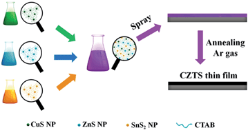
Quaternary kesterite Cu2ZnSnS4 (CZTS) and Cu2ZnSn(S,Se)4 (CZTSSe) thin films have been prepared from a mixture of CuS, ZnS and SnS2 nanoparticles and solar cells were made from the CZTSSe films. The binary sulfide nanoparticles were pre-synthesized in aqueous solution and then spray deposited onto glass substrates. The nano-sized binary sulfide nanoparticles have a large surface area that provides the driving force for solid-state reactions between the nanoparticles and results in the formation of the quaternary CZTS phase at moderate temperatures. The CZTSSe solar cells were prepared using the binary sulfide nanoparticles films annealed in Se vapor and the cells showed an encouraging efficiency of 5.12% (Voc = 378 mV, Jsc = 26.2 mA cm−2 and FF = 51.7%). Our synthetic approach provides a low-cost, environmentally friendly and easy to scale up option for the preparation of CZTSSe thin films for solar cell applications.
:
Zn
:
Sn ratio can be controlled by varying the thickness of each metal layer. More recently, Shin et al. made use of co-evaporation of Cu, Zn, Sn and S followed by annealing to obtain a device with a high efficiency of 8.4% from a device area of 0.45 cm2.12 Despite the excellent progress, vacuum-based techniques still require a high energy input and impose a significant cost on devices. Hence, there is a move towards finding an alternative low-cost fabrication method to the vacuum deposition techniques.
In recent years, there is an increasing amount of work done on the deposition of CZTS thin films using low-cost solution-based methods. Scragg et al. fabricated CZTS thin film solar cells using electrodeposited stacked metal layers and was able to achieve an efficiency of 3.2%.13 Kumar et al. synthesized CZTS thin films by spray pyrolysis, where the precursor solution contained Cu-, Zn-, Sn-salts and thiourea.14,15 The CZTS nanoparticle approach and hybrid solution-particle approach have attracted more interest than other methods due to the possibility of generating solar cells with a high power conversion efficiency – 7.2% for the nanoparticle method and beyond 12.0% for the solution method.16,17 For the CZTS nanoparticle approach, the CZTS nanocrystals have often been synthesized using the hot coordinating solvent method and the nanocrystals then deposited on the substrate and annealed to form the absorber layer.18–22 The hybrid solution-particles approach made use of a slurry containing Cu- and Sn-chalcogenide solution precursors and Zn-chalcogenide nanoparticles dispersed in hydrazine (N2H4), which was then spin-coated and annealed to form the CZTS layer.23
To date, it has been shown that solution processed CZTS solar cells have a reasonably high conversion efficiency and hence considering both device performance and cost, there is potential for this technology to compete with the more mature CdTe and CIGS technologies. The chemicals involved as well as the by-products of the synthesis process have low toxicity which is an added advantage. Since CZTS can be processed in solution, the fabrication process can be easily scaled up for mass production.
There are disadvantages associated with some of the solution deposition processes. Compared to the other solution deposition methods, the electrodeposition method suffers from low conversion efficiency. For the spray pyrolysis method, the NH3 and HCl byproducts generated suggest that this method is less environmentally friendly, especially for large quantity production.24,25 Although the CZTS nanoparticle approach and hybrid solution-particle approach were able produce high efficiency solar cells, both methods have issues that limit large scale practical applications: (i) the use of expensive and toxic organic solvents (oleylamine, hexadecylamine for the former, and hydrazine for the latter) that may increase the fabrication cost and also lead to environmental issues; (ii) highly demanding processing conditions such as high reaction temperature and inert environment make the processes difficult to scale up. Therefore, a novel synthesis method that is cost-effective, environmentally benign and easily up-scalable is required.
Here, we report one such method for the preparation of CZTS thin films. Since Cu2ZnSnS4 is a quaternary compound, instead of using ionic compounds as the precursors, a combination of CuS, ZnS and SnS2 binary sulfide in the ratio 2
:
1
:
1 can be transformed into quaternary films via solid state reactions. These binary sulfide nanoparticles can be easily synthesized in an aqueous environment. This method allows the use of the most common Cu-, Zn- and Sn-precursors including chlorides, sulfates, nitrates and acetates, while the sulfur source is from hydrated sodium sulfide (Na2S·9H2O). The deposition techniques for these solutions could then be spray coating, printing, spin-coating, and many other solution deposition techniques. This route could allow easy tuning of the composition of the films and the possibility of preparing stable inks for printing. Hence, this work paves the way for a large scale and environmentally friendly way to fabricate thin film solar cells.
![]() | ||
| Fig. 1 Experimental method for preparation of CZTS thin films using CuS, ZnS and SnS2 nanoparticles (NP). | ||
Ethanol was used as a solvent in the synthesis of the CZTS thin film because its boiling point is low compared to water thus allowing for a low substrate temperature during the spray process (∼100 °C), minimizing possible oxidation issues. A mixture of CuS, ZnS and SnS2 nanoparticles (molar ratio 2
:
1
:
1) in ethanol was sprayed onto glass substrates and the precursor films were annealed at different temperatures – 200, 300, 400 and 450 °C for 30 min under Ar gas. As shown in Fig. 3, the XRD pattern of the as-deposited precursor film is a composite of the XRD patterns of the CuS, ZnS and SnS2 nanoparticles. After annealing at 200 °C for 30 min, the 2θ peaks at 29.3°, 31.8°, 32.9°, 47.9°, 52.7° and 58.7° became sharper compared to the as deposited precursor film, indicating an increase in the crystallinity of the CuS nanoparticles. Sharp peaks at 28.5°, 47.3° and 56.2° can be observed for samples annealed at 300, 400 and 450 °C, which correspond to the (112), (220) and (312) planes of kesterite CZTS (JCPDS no. 26-0575). In addition to the three major peaks, minor peaks at 18.2°, 23.1°, 33.0°, 69.3° and 76.5° could also be observed for samples annealed at 400 and 450 °C. Therefore, both the major and minor peaks indicate that the CZTS phase has been formed. Comparing the XRD patterns of the films annealed at various temperatures, the full width at half maximum (FWHM) for the (112) peak is found to decrease as the annealing temperature increases from 300 to 450 °C, which indicates that the average CZTS crystallite size in the annealed film increases with annealing temperature.
From the previous discussion, it is evident that the kesterite CZTS phase was formed at temperatures higher than 300 °C. Unfortunately, some binary and ternary phases, Cu2S (JCPDS no. 4-15-2234), ZnS (JCPDS no. 5-0566) and Cu2SnS3 (JCPDS no. 1-089-4714), also share a similar crystal structure, which makes it difficult to conclusively demonstrate the formation of pure CZTS using only XRD data. Raman spectra provide information on the vibrational properties of crystalline samples and are therefore useful for determining the presence of binary and ternary phases in thin films. This technique has been well-established for the identification of impurity phases in CZTS films.28,29 The Raman peaks for CZTS (288, 338 and 368 cm−1), Cu2S (475 cm−1), ZnS (278 and 351 cm−1) and Cu2SnS3 (298 and 356 cm−1) are distinct.30–33 Hence, in order to confirm the phase purity, Raman analysis was performed. As shown in Fig. 4, samples annealed at all three temperatures exhibit a strong peak at 336 cm−1 with two weaker shoulder peaks at 288 and 368 cm−1. The above three peaks are indicative of the presence of the CZTS phase in the films annealed at 300, 400 and 450 °C. The strong peak at 336 cm−1 corresponds to the symmetric A mode vibration.34 In addition, within the resolution of the Raman measurement, no noticeable peaks corresponding to Cu2S (475 cm−1), ZnS (278 and 351 cm−1) or Cu2SnS3 (298 and 356 cm−1) could be observed, which excludes the existence of all three possible impurity phases. Raman analysis thus confirms that pure CZTS films were formed at temperatures higher than 300 °C.
![]() | ||
| Fig. 4 Raman spectra from the films annealed at 300, 400 and 450 °C. The peak position of the 288, 336 and 368 cm−1 lines are marked with vertical dotted lines. | ||
The grain size of the CZTS films is important in determining the performance of the solar cells. In CZTS based thin film solar cells, a large CZTS grain size is favored due to improved charge transport properties as compared to small grain sized films. When annealed at higher temperatures (400 °C), the grain size of the CZTS thin film can reach an average of around 100 nm (Fig. 5a) for a film that is about 1 μm thick (Fig. 5b).
![]() | ||
| Fig. 5 Scanning electron micrographs from the sample annealed at 400 °C. (a) Plan view and (b) cross-sectional view of the as-prepared CZTS thin film. | ||
As the absorption and electrical properties are determined by the composition of the film, it is important to determine the relative elemental composition. The Cu
:
Zn
:
Sn
:
S elemental ratio was determined to be 1.9
:
0.9
:
0.9
:
4.2 for the precursor film using SEM energy-dispersive X-ray spectroscopy (EDS), which is in agreement with the amount of CuS, ZnS and SnS2 added initially. This is close to the starting ratio but slightly rich in S, because the binary sulfide precursors contain excess S due to the oxidation states of the Cu binary compound. After annealing at 400 °C for 30 min, the CZTS films has a Cu
:
Zn
:
Sn
:
S ratio of 1.9
:
1.0
:
0.9
:
4.1, similar to the as-deposited composition. The chemical reaction for the formation of CZTS is proposed to be
![]() | (1) |
Sulfur vapor is formed as a by-product of the reaction. This creates a S-rich environment within the CZTS film, which reduces the need for a sulfurization or selenization process. Generally, CZTS films suffer from loss of Sn and S during annealing.35 From the EDS data, the Sn content in the annealed CZTS films was found to remain fairly constant compared to the precursor film with only a slight S loss. This is mainly due to the relatively low annealing temperature of 400 °C.
For the application in thin film solar cells, the as deposited binary sulfide particles films were thermally annealed at 500 °C for 30 min in an Ar environment after deposition to encourage the inter-diffusion of the elements resulting in the formation of CZTS films. Annealing at this high temperature will allow faster diffusion of the elements and some grain growth. To encourage further grain growth, the film was then selenized in selenium vapour at 520 °C for 12 min. Fig. 6a shows XRD patterns from the annealed film and the selenized film. The XRD pattern from the annealed film matches the kesterite CZTS phase with characteristic 2θ angles of 28.5°, 47.3° and 56.2°. The XRD peaks from the selenized film are shifted to lower 2θ values as compared with the annealed film. The major peak at 28.5° for the CZTS film is shifted by 1° to 27.5° for the CZTSSe film. This is because the smaller sized S atoms are replaced by the larger Se atoms during the selenization process, resulting in larger lattice spacings for CZTSSe than for CZTS.
![]() | ||
| Fig. 6 (a) XRD patterns from a CZTS film prepared by annealing the precursor film at 500 °C and from a CZTSSe film prepared by selenizing the precursor film. (b) Enlargement of the 112 reflection. | ||
Solar cells were fabricated using the selenized film with a Cu-poor and Zn-rich composition. The composition used was Cu/(Zn + Sn) = 0.72 and Zn/Sn = 1.2. The Se/(S + Se) ratio determined by EDX was found to be approximately 0.8. Fig. 7a shows the cross-section of a typical as-prepared CZTSSe solar cell with the configuration – Mo/CZTSSe/CdS/ZnO/ITO/Au. The size of the CZTSSe solar cells (0.11 cm2) were defined by the Au electrode deposition. The current density–voltage (J–V) characteristics for a typical as-prepared CZTSSe solar cell measured in the dark and under AM1.5G illumination are shown in Fig. 7b. The device demonstrates a power conversion efficiency of 5.12% with an open-circuit voltage (Voc) of 378 mV, a short-circuit current density (Jsc) of 26.2 mA cm−2 and a fill factor (FF) of 51.7%. The series resistance (Rs) and shunt resistance (Rsh) are determined to be 3.6 Ω cm2 and 404 Ω cm2 respectively. The device performance is comparable with some of the best performing nanoparticle based CZTSSe solar cells, showing that our approach is highly promising for CZTSSe based solar cells.16,26,27 The thickness of our absorber film was around 800 nm and the grain size less than 500 nm, both of which are well below that for optimum CZTSSe device performance.23 Further optimization could be made by increasing the thickness of the CZTSSe film, which would certainly lead to an improvement in Jsc and hence the efficiency of the solar cell. On top of this, by modifying the film composition as well as the selenization processes, the grain size can be increased and this will lead to an increased photocurrent generation and a reduction in recombination.
![]() | ||
| Fig. 7 (a) Cross-sectional SEM image of the CZTSSe thin film solar cell and (b) J–V curve from the as-prepared CZTSSe solar cells in dark and under AM1.5G illumination. | ||
Fig. 8 shows the external quantum efficiency (EQE) of the CZTSSe based solar cell as a function of photon wavelength. The EQE is fairly high (more than 60%) between 500 to 900 nm. The band gap of the absorber layer is determined to be 1.18 eV by fitting a plot of [hν
ln(1 − EQE)]2 vs. hν near the band edge (inset of Fig. 8). Our calculated band gap matches well with the reported range of 1.0 eV to 1.5 eV for CZTSSe using EQE measurements.36 It is also in good agreement with the band gap of CZTSSe based on optical absorption measurements.37 The band gap estimate based on EQE is reasonable considering the majority of S atoms are replaced with Se during the selenization process.
Footnote |
| † Electronic supplementary information (ESI) available. See DOI: 10.1039/c4ra03349c |
| This journal is © The Royal Society of Chemistry 2014 |