Piezoelectric power generation of vertically aligned lead-free (K,Na)NbO3 nanorod arrays†
Pil Gu Kanga,
Byung Kil Yuna,
Kil Dong Sunga,
Tae Kwon Leea,
Minbaek Leea,
Nuri Leeb,
Seol Hee Ohb,
William Job,
Hae Jin Seogc,
Chang Won Ahnc,
Ill Won Kimc and
Jong Hoon Jung*a
aDepartment of physics, Inha University, Incheon 402-751, Republic of Korea. E-mail: jhjung@inha.ac.kr; Fax: +82-32-872-7562; Tel: +82-32-860-7659
bDepartment of physics, Ewha Womans University, Seoul 120-750, Republic of Korea
cDepartment of Physics and Energy Harvest-Storage Research Center, University of Ulsan, Ulsan 680-749, Republic of Korea
First published on 24th June 2014
Abstract
We report piezoelectric power generation at room temperature, as well as at elevated temperature, using vertically aligned lead-free (K,Na)NbO3 nanorod arrays on a conducting substrate. Ferroelectric (K0.6Na0.4)NbO3 nanorod arrays having a high piezoelectric coefficient of ca. 180 pm V−1 were epitaxially grown on a conducting SrRuO3/SrTiO3 substrate via the facile hydrothermal method at low temperature (ca. 190 °C). After electric poling, the (K,Na)NbO3 nanorod array-based nanogenerator generated a stable high power density of ∼101 μW cm−3 at 20 °C, almost 16 times greater than a BaTiO3 nanowire-based vibrational energy harvester (ca. 6.27 μW cm−3). The (K,Na)NbO3 nanorod array-based nanogenerator exhibited little frequency dependence on external force over a relatively low-frequency range (≤10 Hz) and showed long-term durability even at 100 °C, with a power density of 29 μW cm−3. This work demonstrates the potential of eco-friendly nanogenerators based on (K,Na)NbO3 nanorod arrays for high-output power generation under various environmental conditions.
1. Introduction
Energy harvesting from ambient energy sources such as vibration, heat, and light has attracted a great deal of attention because it provides the means to realise new applications, such as self-powered electronic devices.1,2 For effective conversion of ubiquitous mechanical energy into electricity, in particular, one-dimensional (1-D) piezoelectric/ferroelectric nanostructures have been considered a suitable choice for nanogenerator (NG) applications due to their extremely high piezoelectricity, effective transport of charge carriers, and high sensitivity to small random mechanical disturbances.3 Additionally, the flexibility available for choosing the appropriate piezoelectric and dielectric constants and Curie temperature, simply by tuning the doping parameters and chemical substitution, makes piezoelectric/ferroelectric nanostructure-based NGs useful for high power generation under variable environmental conditions, such as low and high temperatures.4NG application using randomly oriented ferroelectric nanostructures, such as Pb(Zr,Ti)O3 (PZT),5–8 Pb(Mg,Nb)O3–PbTiO3,9 BaTiO3 (BTO),10 ZnSnO3,11,12 LiNbO3,13,14 NaNbO3,15,16 and KNbO3,17 have been reported in numerous studies. However, few works have been reported on NG applications using vertically aligned ferroelectric nanostructures on conducting substrates partly due to the difficulty in synthesis.18–20 Vertically aligned ferroelectric nanostructures provide fundamental insight into the enhancement of conversion efficiency and the application of NG in various environments. Xu et al. reported the chemical synthesis of epitaxial PZT nanowire arrays on conducting Nb:SrTiO3 substrates and their application as high-output converters; the NG, fabricated using a single array of PZT nanowires, produced a peak output voltage of 0.7 V, a current density of 4 μA cm−2, and an average power density of 2.8 mW cm−3.18 Koka et al. reported the synthesis of a polycrystalline BTO nanowire array on a conducting FTO glass substrate and its application as a nano-electromechanical-system vibrational-energy harvester; the electrically poled BTO ferroelectric nanowire arrays produced an average power density of 6.27 μW cm−3 from 1g acceleration, offering a power density 16 times that of ZnO nanowire-based energy harvesters.19 Although the above results are outstanding, environmentally friendly and non-toxic NGs should be explored for high power generation and their broad applications over various environments.21
In this paper, we report the epitaxial growth of vertically aligned lead-free (K,Na)NbO3 (KNN) nanorod (NR) arrays on a conducting SrRuO3/SrTiO3 (SRO/STO) substrate and their application to eco-friendly piezoelectric power generation over a wide temperature range. High-quality single-crystalline KNN NR arrays were obtained via a suitable KOH/NaOH mole ratio and seed layer during a hydrothermal reaction. The KNN NR array exhibited ferroelectricity and a high piezoelectric coefficient, d33 = 180 pm V−1. After electric poling, the KNN NR array-based NG produced an open-circuit voltage of 0.38 V, a closed-circuit current of 6.4 nA (current density: 18.8 nA cm−2), and an average power density of 101 μW cm−3, almost 16 times greater than a BTO nanowire-based vibrational energy harvester. Additionally, the KNN NR array-based NG generated high power density of ca. 29 μW cm−3 at elevated temperatures (∼100 °C). Considering the large piezoelectricity and electro-mechanical coupling constant, and high Curie temperature of KNN, our work demonstrates the potential of KNN NR array-based NGs for high output green power generation over a wide temperature range.
2. Experimental section
Synthesis of KNN NR arrays
A single-crystalline KNN NR array on a SRO/STO substrate was synthesised using the hydrothermal method. In this process, 82.14 mmol KOH (4.609 g, 90%) and 17.8 mmol NaOH (0.7143 g, 98%) were dissolved in 12 mL of distilled (DI) water; 3.76 mmol Nb2O5 (1 g, 99.99%) was then added to the KOH/NaOH solution. After stirring for 2 h, the solution was transferred to a 25 mL Teflon-lined stainless steel autoclave. The KNN seed-layer-coated SRO/STO substrate was positioned face down and placed ∼3 cm above the bottom of the Teflon liner. The 50 nm-thick KNN seed layer and 20 nm-thick SRO film were deposited onto a STO substrate by spin-coating and pulsed laser deposition, respectively.22,23 The hydrothermal reaction was performed at 190 °C for 48 h. After the reaction was complete, the as-grown NR arrays were washed with DI water and dried at 80 °C for 12 h. To remove any possible hydroxyl defects, we further annealed the NR arrays at 600 °C for 12 h.The use of a KNN seed layer and single-crystalline SRO/STO substrate are crucial for pure KNN NR array formation.24 Without the seed layer, only sparse nanoplates formed on the SRO/STO substrate (Fig. S1a in ESI†). Without the single-crystalline SRO/STO substrates, nanoplates significantly aggregated (Fig. S1b in ESI†) and exhibited two phases, i.e., the coexistence of orthorhombic and monoclinic structures (Fig. S1c in ESI†). As shown in Fig. 2S in ESI,† the mole ratio of KOH/NaOH was also crucial to NR morphology; a decrease in the mole ratio resulted in nanoparticle formation instead of NR creation.
Characterisation of KNN NR arrays
The crystallinity and microstructure of the KNN NRs were examined by high-resolution X-ray diffraction (HR-XRD) (Bruker, AXS D8 Discover), field-emission scanning electron microscopy (FE-SEM) (S-4200, Hitachi), and aberration-corrected high-resolution transmission electron microscopy (HR-TEM) (JEM-2100F, Jeol). Just before the HR-TEM measurement, a cross-section of the KNN NR arrays was prepared using a focused ion beam (FIB). The composition of KNN was carefully examined using inductive-coupled plasma (ICP) spectroscopy (Optima 7300DV, Perkin Elmer, Inc.) and electron probe microanalysis (EMPA) (EPMA-1600, Shimadzu). Piezoelectric force microscopy (PFM) (N-Tracer, Nanofocus) was used to investigate the piezoelectricity and piezoelectric/ferroelectric domains. The PFM measurements were performed using an atomic force microscope (AFM) operating at 1 V and 73 kHz. To scan the surface, we used Pt-coated tips and a force constant of 3 N m−1.Fabrication and piezoelectric power measurement of KNN NR-based NG
An Au/Cr-coated Kapton polyimide film (thickness: 125 μm) was attached to the top surface of the KNN as a top electrode. An electric field of ca. 250 kV cm−1 was applied between Au/Cr and the SRO electrodes for electric poling at room temperature.22 NGs were mounted on a custom-designed mechanical system, in which a linear motor was used to periodically apply and release compressive forces to the device. The pushing amplitude and frequency were varied over the course of the measurement, and the input force was instantaneously monitored with a force sensor. The output signal of the piezoelectric device was recorded by low-noise voltage (SR560, Stanford Research Systems) and current preamplifiers (SR570, Stanford Research Systems). For high-temperature measurements, a custom-designed heater was used to adjust the NG temperature, which was monitored by a K-type thermocouple (Fig. S3 in ESI†). All electrical measurements were conducted in a Faraday cage to minimise any undesired noise.3. Results and discussion
Fig. 1a and b show top-view and 45° tilt-view SEM images of KNN NR arrays on a SRO/STO substrate, respectively. All of the KNN NRs were vertically aligned, having a width of ca. 45 nm. Fig. 1c and d show medium- and high-resolution TEM images, respectively, of the cross-section of KNN NR arrays on a SRO/STO substrate. The KNN NRs (height: ca. 280–550 nm) were densely grown on top of the SRO/STO substrate. Based on clear lattice fringe and selected-area electron diffraction (SAED), we concluded that the KNN NRs were single-crystalline and grown along the [001] direction. | ||
| Fig. 1 Vertical alignment and single crystallinity of the (K,Na)NbO3 (KNN) nanorod (NR) arrays on a conducting SrRuO3/SrTiO3 (SRO/STO) substrate. Scanning electron microscopy (SEM) images of (a) top and (b) 45° tilt views. (c) Medium- and (d) high-resolution transmission electron microscopy (TEM) images; in the inset of (d), selected-area electron diffraction (SAED) pattern. (e) Energy-dispersive X-ray spectroscopy (EDX) results for the chemical elements. (f) Spatial dependence of the chemical elements near the interface. In the bottom of (f), a medium-resolution TEM image near the interface is shown. | ||
Because the piezoelectricity and Curie temperature of KNN depends on the mole ratio of K/Na,25 we performed energy-dispersive X-ray spectroscopy (EDX), ICP spectroscopy, and EPMA to examine the chemical composition. While slight variations were observed, all of the results obtained indicated that the KNN NRs consisted of only K, Na, Nb, and O elements (Fig. 1e), with a mole ratio of K![[thin space (1/6-em)]](https://www.rsc.org/images/entities/char_2009.gif) :Na = 0.6:0.4. Consistent with a previous report,26 a large difference in the mole ratio for synthesised KNN NRs (K/Na = 1.5) was observed, as compared with that for the starting material (KOH/NaOH = 4.6). Fig. 1f shows spatial variation in the chemical elements near the interface of KNN NRs on a SRO/STO substrate. The sharp discontinuity of Nb, Ru, and Ti, as well as the continuity of O near the interface, signifies chemical homogeneity and the absence of inter-diffusion during growth.
:Na = 0.6:0.4. Consistent with a previous report,26 a large difference in the mole ratio for synthesised KNN NRs (K/Na = 1.5) was observed, as compared with that for the starting material (KOH/NaOH = 4.6). Fig. 1f shows spatial variation in the chemical elements near the interface of KNN NRs on a SRO/STO substrate. The sharp discontinuity of Nb, Ru, and Ti, as well as the continuity of O near the interface, signifies chemical homogeneity and the absence of inter-diffusion during growth.
High-resolution XRD was performed to reveal the detailed structure of KNN NR arrays on SRO/STO substrates. Fig. 2a and b show the high-resolution XRD for θ–2θ and ϕ scans, respectively. Only the (001), (002), and (003) peaks of KNN (red indices), SRO (green indices), and STO (blue indices) were visible in the θ–2θ scan. Additionally, four KNN peaks were observed at the same ϕ positions of STO in the ϕ scan. These results support the conclusion that single-crystalline KNN NRs were epitaxially grown on the SRO/STO substrate. The epitaxial relationship between KNN NRs and the SRO/STO substrate was (001) KNN ‖ (001) SRO/STO and [100] KNN ‖ [100] SRO/STO.
 | ||
| Fig. 2 Epitaxial growth of the KNN NR arrays on SRO/STO substrates. High-resolution X-ray diffraction (XRD) for (a) θ–2θ, (b) ϕ scans (101 reflection), and (c) reciprocal space mapping (RSM) (−103 reflection) of the KNN NR arrays on a SRO/STO substrate. In the inset of (a), a magnified view of the XRD θ–2θ scan near 2θ = 46° is shown. The red, green, and blue indices represent the peaks of KNN, SRO, and STO, respectively. In (c), r.i.u. represents reciprocal lattice units. | ||
To investigate the epitaxial strain of KNN NRs on SRO/STO, we show the reciprocal space map (RSM) of high-resolution XRD for the (−103) Bragg peaks of KNN and STO in Fig. 2c. The in-plane reciprocal lattice vector (h) of KNN did not coincide with that of STO, which implies the relaxation of compressive strain. From the centre positions of the reciprocal map, the lattice constants of the KNN NRs were estimated to be a = 3.986 Å and c = 4.029 Å. Comparing the lattice constants of (K0.6Na0.4)NbO3 bulk (a = 4.0122 Å, b = 3.9505 Å, and c = 4.0098 Å),27 we noticed that the in-plane lattice contracted, while the out-of-plane lattice became elongated, due to the partial relaxation of compressive strain from the SRO/STO substrate (a = b = c = 3.905 Å).28
The piezoelectricity of KNN NRs was examined using PFM, as schematically shown in Fig. 3a. Before the PFM measurement, we coated 10 nm-thick Pt onto KNN NRs to obtain a uniform electric field and minimise electrostatic effects. Fig. 3b shows the three-dimensional (3-D) topography of KNN NRs. A Pt-coated tip was positioned on top of the NR to measure the current and piezoelectric response when a direct current (dc) voltage was applied. From the current map from conductive AFM and current–voltage (I–V) characteristics (Fig. 3c and d), we confirmed that the leakage current of the KNN NRs was negligible.
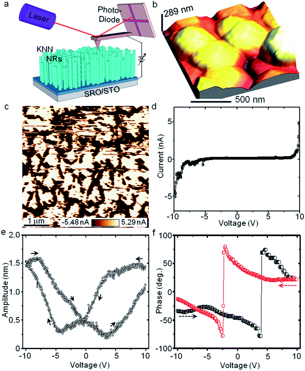 | ||
| Fig. 3 Piezoelectricity/ferroelectricity of KNN NR arrays. (a) Schematic diagram of piezoelectric force microscopy (PFM) measurements. (b) Three-dimensional (3-D) topography of the NR arrays (scanning area: 1 × 1 μm2). (c) Conductive atomic force microscopy (C-AFM) image of the NR arrays for an applied voltage of −1 V. (d) Current–voltage (I–V) characteristics of a NR. Applied direct current (dc) voltage dependences of the piezoelectric (e) amplitude and (f) phase in PFM measurements. | ||
The applied dc voltage dependences of the piezoelectric amplitude and phase are shown in Fig. 3e and f, respectively; the piezoelectric amplitude and phase correspond to the strength of the piezoelectric response and the direction of electric polarisation, respectively.29 With the sweeping of dc voltage, hysteresis of the piezoelectric amplitude was observed, along with abrupt changes in the piezoelectric phase. Such behaviour clearly suggests the switching of domains in KNN, which is generally associated with ferroelectric behaviour.30 The piezoelectric coefficient of the KNN NRs was estimated as d33 = 180 pm V−1 from the linear portion of the piezoelectric amplitude. Comparing the KNN ceramic bulk with the similar mole ratio of K/Na (d33 = 97 pm V−1),31 the significant enhancement in the piezoelectric coefficient of KNN NRs was attributed to the single-crystalline nature of the NRs.
We fabricated the KNN NR array-based piezoelectric NG, as schematically shown in Fig. 4a. The NG device consisted of Au/Cr-coated Kapton polyimide film and KNN NR arrays on a conducting SRO/STO substrate. Due to ferroelectricity, all of the piezoelectric domains in the KNN NR arrays were aligned along the electric-field direction (E) of the poling voltage. Under the application of a uniaxial compressive force F(t), a piezoelectric potential was created inside the KNN NRs. The transient flow of free carriers under an external load screened the piezoelectric potential. When the force was removed, the piezoelectric potential disappeared and the accumulated carriers were released. Thus, the alternating force drove the carriers in the external circuit, creating an alternating voltage and current.32
 | ||
| Fig. 4 Piezoelectric power generation of the KNN NR arrays-based nanogenerator (NG). (a) Schematic diagram of the KNN NR array-based NG. Dark brown, yellow, cyan, light blue, and grey represent the polyimide film, Au/Cr electrode, KNN NRs, SRO electrode, and STO substrate, respectively. (b) Open-circuit voltage and closed-circuit current for specific compressive forces. (c) Compressive force and (d) frequency dependences of the voltage and current for the poled KNN NR array-based NG (solid circles). For comparison, we show the voltage and current for an unpoled KNN NR array-based NG (open rectangles) in (c). Load resistance dependences of (e) the voltage and current and (f) the power density of the poled KNN NR array-based NG. | ||
Fig. 4b shows the open-circuit voltage and closed-circuit current of the KNN NR array-based NG under various compressive forces applied at a frequency of 1 Hz. Using the polarity test, we confirmed that the signal originated from the piezoelectricity of KNN NRs (Fig. S4 in ESI†). With an increase in force, both the voltage and current increased logarithmically rather than linearly (Fig. 4c). A logarithmic increase in the power may be related to the density of the KNN NRs, reducing their susceptibility to large compressive forces. For a compressive force of 1 kgf, values of ca. 0.38 V, 6.4 nA, and 18.8 nA cm−2 were obtained for the voltage, current, and current density of the KNN NR array-based NG, respectively. For comparison, we observed small values for the voltage and current for the unpoled KNN NR array-based NG, which further support the ferroelectricity of KNN NRs. The finite values for the voltage and current may have originated from partial alignment of the piezoelectric domains, due to a self-poling effect, observed in ferroelectric nanostructures.33,34 The poled KNN NR array-based NG generated very stable power for up to at least 105 cycles of 1 kgf compressive force application at a frequency of 1 Hz (Fig. S5 in ESI†). Fig. 4d and S6 in ESI† show the frequency dependence of the open-circuit voltage and closed-circuit current for an amplitude of 1 kgf. Although a slight decrease in the voltage and current was observed below 0.5 Hz, the values obtained for the voltage and current were within 0.37 ± 0.1 V and 6.7 ± 0.5 nA, respectively, over a wide frequency range (0.1–10 Hz).
To further investigate the optimum output power of the KNN NR array-based NG, we conducted electrical measurements by varying the resistance of the external load. The current decreased with an increase in the load resistance due to ohmic loss, and the voltage followed the reverse trend, as shown in Fig. 4e. As a result, the piezoelectric power reached its maximum value for a load resistance of 60 MΩ, corresponding to a peak power density of 101 μW cm−3 (Fig. 4f).
One noteworthy merit of KNN is its relatively high Curie temperature compared with other lead-free ferroelectric materials such as BTO. As a proof of concept, we show the open-circuit voltage and closed-circuit current of the KNN NR array-based piezoelectric NG under high-temperature conditions (Fig. 5a). For all measurements, the compressive force and frequency were set to 1 kgf and 1 Hz, respectively. With an increase in temperature, the output power slowly decreased initially but rapidly decreased above 60 °C (Fig. 5b). For example, the piezoelectric power at 20 °C was reduced to 92% at 60 °C, but 30% at 100 °C. However, the KNN NR array-based NG generated stable power for up to 105 cycles of compressive force, even at 100 °C (Fig. 5c).
 | ||
| Fig. 5 Performance of the KNN NR array-based NG at elevated temperatures and its long-term durability at high temperature. (a) Open-circuit voltage and closed-circuit current versus temperature. (b) Temperature dependences of the voltage and current for the KNN NR array-based NG (solid circles). For comparison, we show the voltage and current for the KNN NR array-based NG with Pt electrode on Si substrate (open circles) in (b). (c) Long-term durability test of the KNN NR array-based NG at 100 °C over 105 cycles. | ||
To understand the rapid decrease in the piezoelectric power above 60 °C, we replaced the top electrode of the Au/Cr-coated Kapton film with a Pt-coated Si substrate in the KNN NR array-based NG; the temperature dependence of the piezoelectric power is shown in Fig. 5b and S7 in ESI.† The Pt-coated Si electrode resulted in smaller piezoelectric power compared with the Au/Cr-coated Kapton electrode, most likely due to the inability of the rigid Si substrate to deliver compressive force to short KNN NRs. The lower electrical conductivity and higher work function of Pt than Au might also affect the smaller piezoelectric power.35 However, the piezoelectric power for the Pt-coated Si electrode showed much slower temperature dependence than did the Au/Cr-coated Kapton electrode. This result implies that the origin of the rapid decrease in the piezoelectric power above 60 °C in Fig. 5b was partially related to the mechanical behaviour of the polymer substrate such as decreased Young's modulus of Kapton and reduced adhesion of Au/Cr due to shrinkage/expansion of Kapton.36 On the other hand, the slow decrease in the piezoelectric power, even for the Pt-coated Si top electrode, implies that other effects also influenced the piezoelectric power at high temperatures. In ferroelectric materials, the piezoelectric coefficient usually decreases with increasing temperature and disappears above the Curie temperature, whereas the dielectric constant increases with increasing temperature and then decreases above the Curie temperature.37 Considering the fact that piezoelectric power is proportional to the square of the piezoelectric coefficient divided by the dielectric constant,9,19 the origin of the rapid decrease in the piezoelectric power above 60 °C in Fig. 5b must also be partially related to the temperature dependences of the piezoelectric coefficient and the dielectric constant of KNN NRs.
Compared with PZT and BTO arrays,18,19 there are several advantages of KNN NR array-based NGs. While the PZT nanowire-based NG showed higher average power density (ca. 2.8 mW cm−3) compared with that of KNN (101 μW cm−3) and BTO (6.27 μW cm−3) at room temperature, PZT contains more than 60 wt% lead oxide. Thus, due to the restricted use of certain hazardous substances in electronic equipment, toxic lead-containing PZT nanowire-based NGs should be replaced by lead-free equivalents.38 While both KNN and BTO are lead-free piezoelectric materials and have similar piezoelectricity values, KNN has a higher Curie temperature (∼420 °C) than BTO (∼135 °C).38,39 The piezoelectricity becomes diminished above the Curie temperature; thus, the KNN NR array-based NG may be more stable than a BTO-based vibrational-energy harvester at high temperatures and under thermal fluctuation. Additionally, single-crystalline KNN NRs should be more efficient high-power NGs than polycrystalline BTO nanowires are. Moreover, the piezoelectricity of the KNN NR array can be enhanced by fine tuning the K/Na mole ratio of 1.0,25 as well as by adjusting the epitaxial strain of the conducting substrate.40 Thus, KNN NR array-based NGs may provide superior performance as an eco-friendly piezoelectric power generator in various environments.
Compared with randomly oriented ferroelectric nanostructures, such as LiNbO3,13 NaNbO3,15 and KNbO3,17 there are several advantages of KNN NR array-based NGs. Randomly oriented ferroelectric nanostructures were usually mixed with polymer, such as polydimethylsiloxane (PDMS) for NG applications. Since PDMS is rather weak for heat and organic solvent, mixed composite may not serve as NG at high temperature and in a certain chemical condition. In addition, the piezoelectric output was strongly dependent on the volume ratio and the spatial distribution of ferroelectric nanostructures in mixed composite. Therefore, KNN NR array-based NGs may provide more fundamental insight into the enhancement of piezoelectric power and better performance at harsh environment than randomly oriented ferroelectric nanostructure based NG.
4. Conclusions
We demonstrated the high performance of piezoelectric power generation for lead-free KNN NR array-based NGs. A single-crystalline (K0.6Na0.4)NbO3 NR array was epitaxially grown on a conducting SrRuO3/SrTiO3 substrate via a simple hydrothermal method at low temperature (ca. 190 °C). The KNN NR array exhibited a high piezoelectric coefficient, d33 = 180 pm V−1, and switching of the electric polarisation direction through application of an external voltage. For 1 kgf of external compressive force, the KNN NR array-based NG generated an open-circuit voltage of 0.38 V, a closed-circuit current of 6.4 nA, a current density of 18.8 nA cm−2, and a power density of 101 μW cm−3. The KNN NR array-based NG exhibited little frequency dependence on the external force and showed long-term durability even at 100 °C, with a power density of 29 μW cm−3. Considering the ease in fine tuning the mole ratio of K/Na, the crystalline direction, and Curie temperature of the NRs, the KNN NR array-based NG has great potential for high output power generation under harsh environmental conditions, with a wide temperature range. Moreover, the lead-free KNN NR array-based NG will offer a readily available solution for current piezoelectric energy harvesting technology to comply with future environmental regulations.Author contributions
JHJ designed the research. PGK and BKY prepared the nanorod and performed the SEM and TEM measurements. KDS and TKL performed XRD and RSM measurements, and grew SRO thin films on STO substrate using pulsed laser deposition. PGK, BKY and ML fabricated the nanogenerator and tested the performance. NL, SHO and WJ carried out the PFM measurements and analysis. HJS, CWA and IWK grew KNN seed layer on SRO/STO substrate using spin-coating. PKG, ML and JHJ wrote the manuscript. All authors read and approved the final manuscript.Acknowledgements
This research was supported by Basic Science Research Program through the National Research Foundation of Korea (NRF) funded by the Ministry of Education, Science and Technology (2012R1A1A2002536 and 2013R1A2A2A01015734).Notes and references
- M. S. Dresslhaus and I. L. Thomas, Nature, 2001, 414, 332–337 CrossRef PubMed.
- Z. L. Wang, Sci. Am., 2008, 298, 82–87 CrossRef PubMed.
- Z. L. Wang and J. H. Song, Science, 2006, 312, 242–246 CrossRef CAS PubMed.
- B. Jaffe, W. Cook and H. Jaffe, Piezoelectric Ceramics, Academic Press, London, 1971 Search PubMed.
- X. Chen, S. Xu, N. Yao and Y. Shi, Nano Lett., 2010, 10, 2133–2137 CrossRef CAS PubMed.
- W. Wu, S. Bai, M. Yuan, Y. Qin, Z. L. Wang and T. Jing, ACS Nano, 2012, 6, 6231–6235 CrossRef CAS PubMed.
- Y. Chen, T. Liu, C. Chen, C. Liu, S. Chen, W. Wu, Z. L. Wang, J. He, Y. Chu and Y. T. Chueh, ACS Nano, 2012, 6, 2826–2832 CrossRef CAS PubMed.
- J. Kwon, W. Seung, B. K. Sharma, S. Kim and J. Ahn, Energy Environ. Sci., 2012, 5, 8970–8975 CAS.
- S. Xu, Y.-W. Yeh, G. Poirier, M. C. McAlpine, R. A. Register and N. Yao, Nano Lett., 2013, 13, 2393–2398 CrossRef CAS PubMed.
- K.-I. Park, S. Xu, Y. Liu, G. T. Hwang, S. J. L. Kang, Z. L. Wang and K. J. Lee, Nano Lett., 2010, 10, 4939–4943 CrossRef CAS PubMed.
- J. M. Wu, C. Xu, Y. Zhang, Y. Yang, Y. Zhou and Z. L. Wang, Adv. Mater., 2012, 24, 6094–6099 CrossRef CAS PubMed.
- K. Y. Lee, D. Kim, J.-H. Lee, T. Y. Kim, M. K. Gupta and S.-W. Kim, Adv. Funct. Mater., 2014, 24, 37–43 CrossRef CAS.
- B. K. Yun, Y. K. Park, M. Lee, N. Lee, W. Jo, S. Lee and J. H. Jung, Nanoscale Res. Lett., 2014, 9, 4 CrossRef PubMed.
- Z. Chen, J. Huang, Y. Yang, Y. Wang, Y. Wu, H. He, X. Wei, Z. Ye, H. Zeng, H. Cong and Z. Jiang, RSC Adv., 2012, 2, 7380–7383 RSC.
- J. H. Jung, M. Lee, J.-I. Hong, Y. Ding, C.-Y. Chen, L.-J. Chou and Z. L. Wang, ACS Nano, 2011, 5, 10041–10046 CrossRef CAS PubMed.
- W. Zeng, X.-M. Tao, S. Chen, S. Shang, H. L. W. Chan and S. H. Choy, Energy Environ. Sci., 2013, 6, 2631–2638 CAS.
- J. H. Jung, C.-Y. Chen, B. K. Yun, N. Lee, Y. Zhou, W. Jo, L.-J. Chou and Z. L. Wang, Nanotechnology, 2012, 23, 375401 CrossRef PubMed.
- S. Xu, B. J. Hansen and Z. L. Wang, Nat. Commun., 2010, 1, 93 CrossRef PubMed.
- A. Koka, Z. Zhou and H. A. Sodano, Energy Environ. Sci., 2014, 7, 288–296 CAS.
- S. Kim, J.-H. Lee, J. Lee, S.-W. Kim, M. H. Kim, S. Park, H. Chung, Y.-I. Kim and W. Kim, J. Am. Chem. Soc., 2013, 135, 6–9 CrossRef CAS PubMed.
- C. R. Bowen, H. A. Kim, P. M. Weaver and S. Dunn, Energy Environ. Sci., 2014, 7, 25–44 CAS.
- C. W. Ahn, S. Y. Lee, H. J. Lee, A. Ullah, J. S. Bae, E. D. Jeong, J. S. Choi, B. H. Park and I. W. Kim, J. Phys. D: Appl. Phys., 2009, 42, 215304 CrossRef.
- K. D. Sung, Y. A. Park, N. Hur, J. H. Jung, D. H. Kim and B. W. Lee, Curr. Appl. Phys., 2014, 14, 251–253 CrossRef PubMed.
- Y. Xu, Q. Yu and J. Li, J. Mater. Chem., 2012, 22, 23221–23226 RSC.
- Y.-J. Dai, X.-W. Zhang and K.-P. Chen, Appl. Phys. Lett., 2009, 94, 042905 CrossRef PubMed.
- Z. Wang, H. Gu, Y. Hu, K. Yang, M. Hu, D. Zhou and J. Guan, CrystEngComm, 2010, 12, 3157–3162 RSC.
- J. Tellier, B. Malic, B. Dkhil, D. Jenko, J. Cilensek and M. Kosec, Solid State Sci., 2009, 11, 320–324 CrossRef CAS PubMed.
- Y.-H. Chu, M. P. Cruz, C.-H. Yang, L. W. Martin, P.-L. Yang, J.-X. Zhang, K. Lee, P. Yu, L.-Q. Chen and R. Ramesh, Adv. Mater., 2007, 19, 2662–2666 CrossRef CAS.
- A. Gruverman and S. V. Kalinin, J. Mater. Sci., 2006, 41, 107–116 CrossRef CAS.
- S. Jesse, A. P. Baddorf and S. V. Kalinin, Appl. Phys. Lett., 2006, 88, 062908 CrossRef PubMed.
- Y. Guo, K.-I. Kakimoto and H. Ohsato, Appl. Phys. Lett., 2004, 85, 4121–4123 CrossRef CAS PubMed.
- Y. Zhang, Y. Liu and Z. L. Wang, Adv. Mater., 2011, 23, 3004–3013 CrossRef CAS PubMed.
- P. Yu, W. Luo, D. Yi, J. X. Zhang, M. D. Rossell, C.-H. Yang, L. You, G. Singh-Bhalla, S. Y. Yang, Q. He, Q. M. Ramasse, R. Erni, L. W. Martin, Y. H. Chu, S. T. Pantelides, S. J. Pennycook and R. Ramesh, Proc. Natl. Acad. Sci. U. S. A., 2012, 109, 9710–9715 CrossRef CAS PubMed.
- B. C. Jeon, D. Lee, M. H. Lee, S. M. Yang, S. C. Chae, T. K. Song, S. D. Bu, J.-S. Chung, J.-G. Yoon and T. W. Noh, Adv. Mater., 2013, 25, 5643–5649 CrossRef CAS PubMed.
- H.-K. Park, K. Y. Lee, J.-S. Seo, J.-A. Jeong, H.-K. Kim, D. Choi and S.-W. Kim, Adv. Funct. Mater., 2011, 21, 1187–1193 CrossRef CAS.
- Technical data sheet of polyimide film, http://www2.dupont.com/Kapton/en_US/.
- T. Leist, J. Chen, W. Jo, E. Aulback, J. Suffner and J. Rödel, J. Am. Ceram. Soc., 2012, 95, 711–715 CrossRef CAS PubMed.
- Y. Saito, H. Takao, T. Tani, T. Nonoyama, K. Takatori, T. Homma, T. Nagaya and M. Nakamura, Nature, 2004, 432, 84–87 CrossRef CAS PubMed.
- J. Li, K. Wang, F. Zhu, L. Cheng and F. Yao, J. Am. Ceram. Soc., 2013, 96, 3677–3696 CrossRef CAS PubMed.
- C. Daumont, W. Ren, I. C. Infante, S. Lisenkov, J. Allibe, C. Carrétéro, S. Fusil, E. Jacquet, T. Bouvet, F. Bouamrane, S. Prosandeev, G. Geneste, B. Dkhil, L. Bellaiche, A. Barthélémy and M. Bibes, J. Phys.: Condens. Matter, 2012, 24, 162202 CrossRef CAS PubMed.
Footnote |
| † Electronic supplementary information (ESI) available: effects of the seed layer and substrate, KOH/NaOH mole ratio for morphology and phase of the NR arrays, piezoelectric power measurement system at elevated temperature, polarity reversal test of the piezoelectric signal, long-term durability test of the NG at 20 °C, frequency dependence of the piezoelectric power, temperature dependent piezoelectric voltage and current for Pt-coated Si top electrode. See DOI: 10.1039/c4ra02921f |
| This journal is © The Royal Society of Chemistry 2014 |