Magnetically enhanced plasma coating of nanostructures with ultrathin diamond-like carbon films
J. D. Beard†
a,
S. Aleksandrovb,
C. H. Walkerb,
D. Wolversona,
J. M. Mitchelsc and
S. N. Gordeev*a
aDepartment of Physics, University of Bath, Claverton Down, Bath, BA2 7AY, UK. E-mail: s.gordeev@bath.ac.uk
bDiamond Hard Surfaces Ltd, Towcester, NN12 8EQ, UK
cMicroscopy and Analysis Suite, University of Bath, Claverton Down, Bath, BA2 7AY, UK
First published on 6th June 2014
Abstract
Diamond-like carbon (DLC) films are widely used as protective coatings in a variety of technical macro- and micro-applications. However, most of the widely-used coating methods are not suitable for nanoscale applications. In this work, the method of magnetically enhanced plasma deposition (MEPCVD) was employed for the coating of AFM probes and free-standing nanostructures with 3–20 nm thick DLC films. The carbon bonding structure, mechanical and tribological properties of the films as well as the anisotropy of the coatings and its effect on the shape of nanoscale features were investigated and it is shown that the method employed produces very smooth coatings (roughness below 0.2 nm) with a significantly lower than usual internal stress of 0.5–0.8 GPa. Wear tests of AFM probes at a high load (1 μN) showed that the DLC coating decreases their wear rate by two orders of magnitude. It was found that coating of free-standing nanostructures even with ultrathin DLC films may cause their deformation due to the interface stress when the coating is asymmetric.
1. Introduction
Diamond-like carbon (DLC), a metastable alloy of graphitically (sp2) and diamond (sp3) bonded carbon atoms, often also incorporating hydrogen atoms, is known under many different names: amorphous diamond, diamond hard carbon, tetrahedrally bonded amorphous carbon etc. The long list of different names reflects the fact that, due to the metastable nature of this material, its mechanical and tribological properties highly depend on the method of fabrication. Out of dozens of methods currently used probably the most well-known are ion-beam1 and mass selected ion beam2 deposition, vacuum arc discharge,3,4 sputtering,5 pulsed laser6 and plasma-based7,8 deposition techniques.Due to its extreme hardness, good wear resistance, low friction, high thermal conductance, chemical inertness and biocompatibility, DLC is widely used in science and technology as a protective coating for mechanical parts and tools,9 optical devices,10 magnetic storage disks,11,12 biomedical implants13–15 and solar cells.16 Coating even with a very thin layer (∼1–10 nm) of DLC often results in very efficient protection of the sample surface. This property makes ultrathin DLC films a very promising candidate for a variety of emerging applications in nanoscience and nanotechnology. The computer industry has used DLC coatings for protection of hard disks for a long time but applications of DLC in other micro- and nanoscale devices (e.g. MEMS and NEMS) still need to be explored.17 Many electronic and magnetic storage applications require very thin protective coatings. For example, for head/disk interface the coating should be ∼2–3 nm thick.11,18 High wear resistance is very important for many applications of nanotools, in particular in mechanical nanolithography, where the required pattern is created either by removing (e.g. scratching) off some material19 or by imprinting nanoscale features on a layer of a photoresist with a sharp tip.20,21
Recently, several research groups have reported their investigations of ultrathin DLC films fabricated by ion beam deposition,22 electron cyclotron resonance chemical vapour deposition (ECR-CVD)23 and Filtered Cathodic Vacuum Arc (FCVA) discharge23,24 techniques. These studies showed that DLC films can be used as a protective coating for a new generation of high-density magnetic memory disks. It was found that, depending on the deposition method, DLC coatings form a continuous film for thicknesses either above 2 nm (FCVA) or above 5 nm (ECR-CVD). For continuous films, very smooth (∼0.1 nm roughness) coatings can be obtained.23,24 The composite hardness and Young's modulus of the films was found to decrease with decreasing thickness of the films.12,25 However, all these studies were performed on flat surfaces and did not cover the properties of coated nanostructures.
One of the potential areas of applications for ultrathin carbon films is the mechanical and chemical protection of probes for Atomic Force Microscopy (AFM). AFM is a very popular instrument for nanoscale characterisation of material surfaces. The applications of AFM have quickly expanded in the last 10 years, especially after the development of novel measurement modes allowing measurement not only of the sample's topography but also of its nanoscale chemical and physical properties. Some of these modes (e.g. contact mode, force spectroscopy, measurements of electrical conductance etc.) require keeping the AFM probe in contact with the sample surface during measurements. This causes rapid wearing of the AFM probes. The commonly used materials for fabrication of AFM probes are crystalline Si and Si3N4 which have relatively good wear properties but are significantly worse than that of DLC. However, AFM probes for studies of electrical conductance or magnetic properties are usually coated with metals that have poor wear resistance. It was demonstrated that coating of AFM probes with DLC drastically increases their wear resistance.26 Several commercial companies (e.g. Bruker, NT-MDT, Budget Sensors, NanoWorld) are now producing DLC-coated AFM probes.
For nanoscale applications, protective coatings should satisfy several specific requirements that may not be very important for large-scale applications. In particular, the protective film should have low surface roughness and cause low mechanical stress. Several popular deposition methods give cobblestone-like coatings with the cobbles being clusters of sp3 bonded carbon. The size of the cobbles depends on the method and deposition parameters and usually is larger than 10–100 nm,27 which does not make such films attractive for ultrathin coatings. The other major problem of DLC coatings is their very large (up to 10 GPa) residual mechanical stress. In large-scale applications, this induces delamination of the coatings from the surface of the substrate, while in micro- and nanoscale applications this usually causes bending of the coated structures.28 In macro applications, the delamination can be prevented by increasing adhesion, using an intermediate buffer layers.29 For example, a 400 nm thick sublayer of Ti gives a very effective bonding of DLC to steel.30 However, this technique, due to the large thickness of the required buffer layer, cannot be used for nanostructures. One of the usual methods of preventing micro/nanostructures from deformation is rotation of the sample during coating to ensure uniform coating of all sides.4 However, this method does not work in cases of closely standing high-aspect-ratio structures, as they create shadow areas that are not accessible for deposition. Thus methods of low-stress coating are currently in great demand. Also, it would be beneficial to use a low temperature deposition technique, as for high-temperature coatings the deposited carbon may form carbide with the material of the substrate. For example, for deposition on silicon, a formation of a substantial layer of silicon carbide at the carbon–silicon interface with the thickness of 5–10 nm has been reported.31
In this paper, a magnetically enhanced plasma-assisted chemical vapour deposition method was employed to explore coating of nanostructures with DLC films of 3–30 nm in thickness. Using the magnetic field allows achievement of longer electron path lengths thus encouraging a higher plasma ionisation.32 This results in a higher hardness and Young's modulus, and lower surface roughness in comparison with the DLC films fabricated by the conventional PECVD system.33 Also this method allows the deposition of films that stay stable and do not show any signs of delamination up to much thicker coatings (∼100 μm), thus implying a good adhesion and low internal stress of the deposited material. We employed this method for coating of a variety of AFM probes and specially grown free-standing nanostructures. The coatings were characterised by Raman spectroscopy as well as electron and atomic force microscopy; elastic moduli and internal stresses of the films were determined and wear resistance tested.
2. Experimental details
DLC films were fabricated using a process employing a magnetically enhanced plasma deposition (MEPCVD) method described elsewhere.34 In brief, the deposition was performed in a vacuum chamber with the base pressure below 10−8 Torr. The samples were initially cleaned by Kr plasma etching during 15 min. Deposition was performed using a Direct Current (DC) hydrocarbon plasma in a linear magnetic field that was applied between the anode and cathode. Using the linear magnetic field orthogonal to the surface of the substrate allows deposition of low stress coatings and improvement of the smoothness of the deposited films.33 The method employed gives high-quality DLC coatings, with a hardness above 40 GPa, on a wide variety of substrates (steel, ceramics, plastics) at around 100 °C and can be applied up to 70 or 80 microns on these same materials, depending on the substrate geometry. This is much thicker than typically can be achieved by many other deposition methods (∼6 μm) for example using sputtering. The fact that these thick films do not delaminate indicated both good adhesion to the surface and low mechanical stress of the deposited DLC films. The good adhesion of the material is due at least in part to the relatively low deposition temperature. For such films, the coefficient of friction against dry steel was found to be ∼0.07–0.08 or as low as 0.025 against itself at a high pressure (>3 GPa).For ultrathin (3–30 nm) coatings, the parameters of the deposition process were optimised to get low roughness and even coating. A linear magnetic field in the range of 10–200 mT was used. The voltage applied between the anode and cathode was 1.5 kV. A disassociated hydrocarbon was used as a precursor gas and the substrate temperature was 90 °C during deposition.
Thickness of the coatings was determined from transmission electron microscopy (TEM) images of the coated AFM probes, using JEOL JEM1200EXII electron microscope with an electron beam energy of 120 kV. This method enabled us to analyse thickness variations of the coating on the AFM probe surface. A low dose method was employed to ensure minimal damage during measurement.
In total, coating of 25 silicon and silicon nitride AFM probes, produced by Budget Sensors and Bruker, was investigated. The probes had large variations in the tip radius (3–20 nm), thickness of cantilevers (0.45–4 μm) and spring constants (0.02–70 N m−1). Deposition was performed on the working side of the AFM probes (where the tip is located).
AFM imaging of DLC coatings and wear resistance studies were performed using a Digital Instruments multimode scanning probe microscope equipped with a NanoScope IIIA controller. Pseudo-3D AFM images were plotted using the WSxM software from Nanotec Electronica S.L.35 and Gwyddion sortware.36
Raman spectroscopy was performed at two excitation wavelengths at 325 nm (HeCd Kimmon Laser) and 532 nm (Renishaw Diode Laser) with a Renishaw inVia microspectrometer. For the 325 nm a NUV ×40 (Thorlabs) objective was used and for the 532 nm a 50× Planupol 0.78NA objective was chosen (Leica). The laser power at the sample was kept below 10 mW. DLC films for these measurements were deposited on substrates cleaved from a 〈100〉-oriented single-crystal silicon wafer (IDB Technologies Ltd).
Free-standing nanostructures were fabricated using the electron-beam-induced deposition (EBID) technique described in detail in our earlier paper.19 For convenient handling, these structures were grown on the tips of AFM probes. The growth was performed in the vacuum chamber of a scanning electron microscope (Hitachi 5300SE FESEM) at a base vacuum of 0.01 Pa, using an electron beam energy of 20 kV and a beam current of 0.1 nA. No precursor gas was used for this purpose. It is known that in such conditions the source of the growth material is the residual gas of hydrocarbon molecules, which are present in the vacuum chamber of the microscope. The electron beam, entering the sample, produces secondary electrons, which interact with hydrocarbon molecules adsorbed on the surface of the sample. The secondary electrons decompose hydrocarbon molecules; the lighter, volatile fraction is pumped away, while the heavier fraction is deposited on the sample surface. The deposited material is composed of mainly amorphous carbon with a small proportion of oxygen and hydrogen.37
3. Results and discussion
3.1 Carbon bonding structure
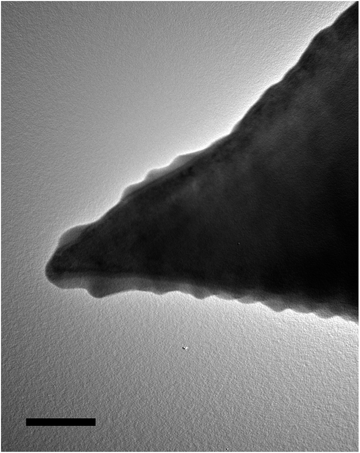
The method of DLC deposition employed gave continuous, pinhole free coatings for all thicknesses in the range of 3–80 nm used in our work. The thickness of the DLC films was determined from transmission electron microscopy (TEM) images, on which DLC shows clear contrast when deposited on silicon or silicon nitride (see Fig. 1). The electron diffraction analysis of the DLC films did not show any structure indicating that they are amorphous.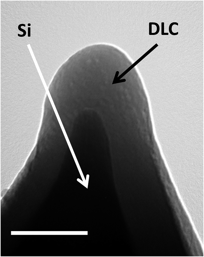 | ||
| Fig. 1 TEM image of the extremity of a silicon AFM probe coated with a DLC film. Scale bar is 100 nm. | ||
The mechanical properties of DLC films are known to depend strongly on the type of C–C bonding. Graphitically bonded carbon (sp2) is soft while the diamond-bonded carbon (sp3) is extremely hard. Usually, the higher the sp3/sp2 ratio, the closer are the mechanical properties of the DLC material to that of diamond. However, sp3 bonding is metastable compared to sp2 bonding, so it needs to be stabilised. This can be achieved by C–H bonds, so hydrogen is often deliberately added to improve mechanical properties of DLC films.38 Apart from stabilising sp3 bonds, hydrogen also passivates dangling bonds, reducing surface interaction and improving strain tolerance of the coating. All this leads to a combination of low friction and high wear resistance under a wide range of sliding contact conditions. In particular, hydrogenated DLC shows much better tribological performance than hydrogen-free films in dry or inert atmosphere.
Raman spectroscopy is probably the most common technique for evaluation of the bonding structure of carbon in DLC films. For hydrogenated DLC films, multi-wavelength Raman studies usually give more reliable results than single-wavelength measurements.39 To obtain information about the bonding structure of our samples, we measured Raman spectra for two excitation wavelengths: λ1 = 325 nm and λ2 = 532 nm. Fig. 2 shows such spectra for 20 and 10 nm thick DLC films deposited on a crystalline silicon substrate. These spectra are similar to published data for thick plasma-deposited DLC films. Raman spectra of disordered carbons are known to be dominated by two modes, which are usually called G (around 1580 cm−1) and D (around 1350 cm−1) modes.39 For the 10 nm film, an additional peak at approximately 960 cm−1 can be seen in the spectrum obtained for the excitation wavelength of 532 nm. This is the second order phonon scattering from the silicon substrate, that can be observed due to the high transparency of the film. The D peak is related to the presence of those sp2 bonds forming aromatic rings, while G peak is due to sp2 bonds of both types, chains and rings. The positions, widths and magnitudes of these peaks are determined by the structure of the sp2 clusters which is in turn related to the sp3 content of the film. As shown by Cui et al.40 the dispersion of the G peak in plasma-deposited (hydrogenated) DLC is a linear function of the total sp3 content, where the total sp3 content is the sum of C–C and C–H sp3 bonds, and can be described by the following empirical relation:
 | (1) |
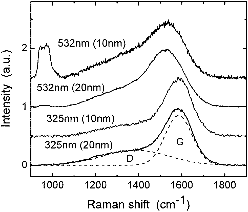 | ||
| Fig. 2 Raman spectra of 10 and 20 nm thick DLC films for excitation 532 nm and 325 nm. Dashed lines show an example of Gaussian fit for the D and G peaks. Curves are shifted vertically for clarity. | ||
Thus measuring positions of the G peak for two different excitation wavelengths the total sp3 content in the sample can be determined. To find positions of the peaks we first removed linear background and then fitted spectra with two Gaussian peaks (D and G). Using the formula above, the sp3 content of 56% and 54% was obtained for 20 nm and 10 nm thick films, respectively. The accuracy of the ‘dispersion method’ as stated by Cui et al.40 is ∼6%.
For ultrathin DLC films, the sp3 content usually decreases with decreasing the thickness of the film, especially below 10 nm.12,25 This is believed to be due to the mechanism of the sp3-bond formation.38 In the process of fabrication, the deposited carbon atoms first form more energetically favourable sp2 bonds, which are then bombarded by energetic ions from plasma. This bombardment provides an additional energy required for transforming sp2 bonds into sp3. Thus the surface layer of DLC has a higher sp2/sp3 ratio than the deeper volume and so ultrathin DLC films tend to have lower concentration of sp3 bonds than thicker films.
The same dispersion data can also be used to estimate the hydrogen content in the samples using calibration graphs presented in ref. 39. Such analysis gives 22–26% for the hydrogen content in our samples.
3.2 Surface roughness
Very often, the roughness of DLC films is estimated by comparing surface topography of coated and uncoated polished silicon wafers.41 This methods works well when intrinsic roughness of the DLS film significantly exceeds the original roughness of the polished silicon substrate. However, for very smooth DLC films, this method becomes unreliable. We performed our roughness measurements using mica instead of silicon. Mica is a two-dimensional material that can be easily cleaved to obtain a very smooth (virtually atomically flat) surface, so the roughness of the coating is defined by the roughness of the deposited layer rather than the roughness of the substrate. Fig. 3 shows AFM images of uncoated mica (a) and two coated samples with the thickness of DLC films of 10 nm (b) and 20 nm (c). The shown sample of mica has two atomically flat areas, one of which is just one atomic layer thicker than the other. Coated samples have clearly rougher surface. Fig. 3c shows height distribution diagrams for the three samples. The 20 nm film is slightly rougher than the 10 nm film with rms values of 0.18 and 0.15 nm, respectively, per 0.24 × 0.24 μm2 area. These results show that the employed method of deposition gives very smooth DLC coatings with ultralow roughness.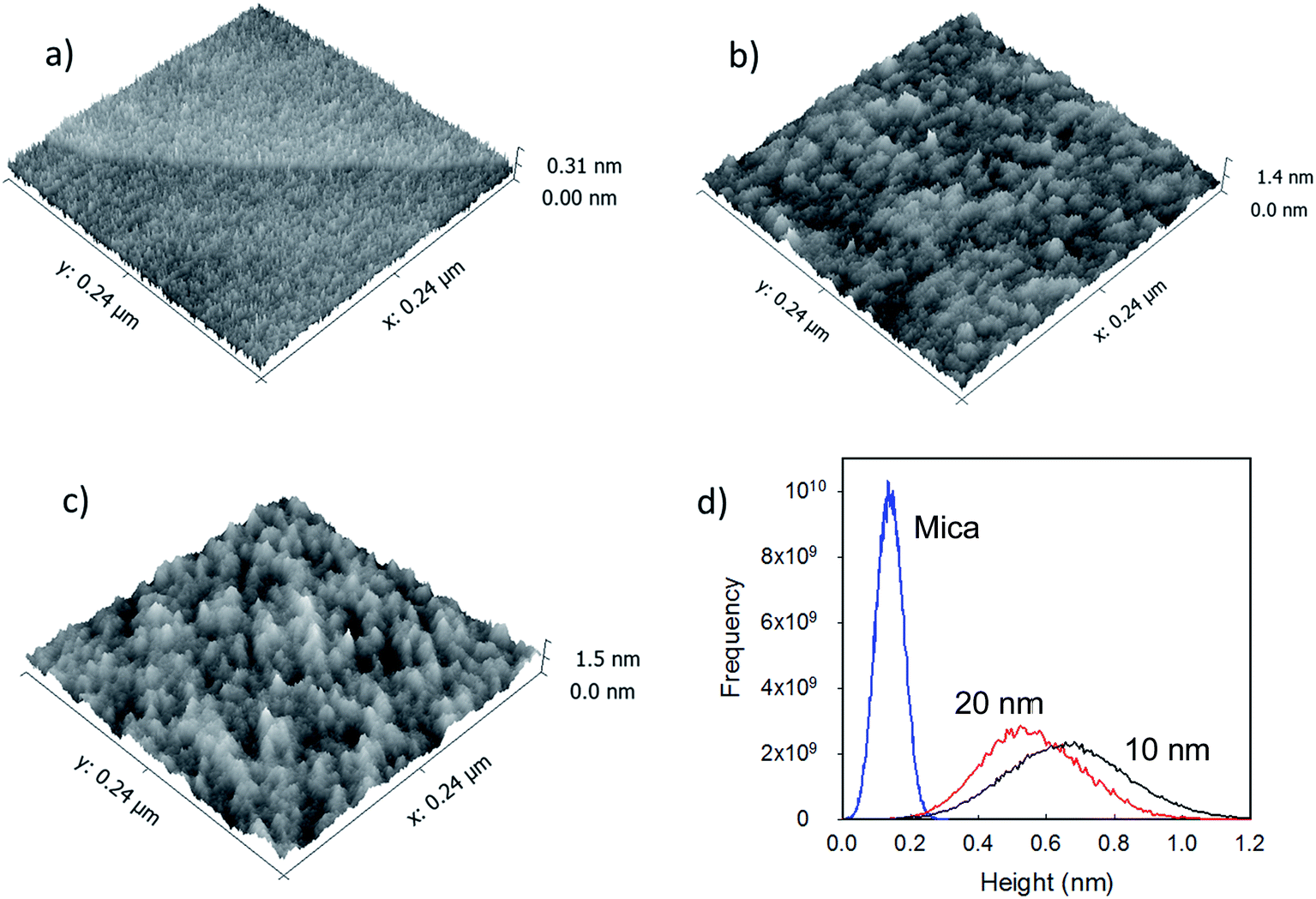 | ||
| Fig. 3 Pseudo 3D AFM images of (a) uncoated mica, (b) 10 nm DLC and (c) 20 nm DLC layers. (d) Height distribution roughness diagrams for these samples. | ||
TEM imaging of coated AFM probes (see Fig. 4) shows that the DLC layer is smoother on the surfaces which are oriented perpendicular to the direction of deposition (the probes' apex in this case) and rougher at the pyramidal sides of the probes.
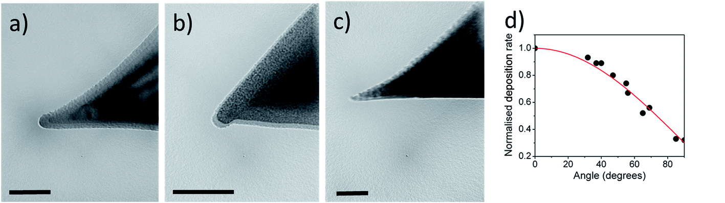 | ||
| Fig. 4 (a–c) TEM images of AFM probes coated with DLC films. (d) Normalised deposition rate as a function of deposition angle. Scale bar is 100 nm. | ||
3.3 Anisotropy of coating
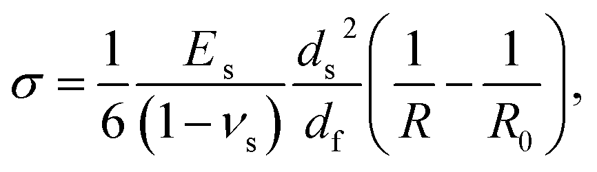
Coating usually changes the geometry of sharp features. To study this effect, we analysed how the DLC coating affects the radius of curvature of AFM tips and the shape of nanopillars. The radius of curvature of the apex is an important parameter of an AFM probe because it limits the minimum size of a surface feature that can be resolved and therefore determines spatial resolution of the probe. Previous studies4 showed that in the case of a uniform coating (the samples were rotated during deposition) and for comparatively thick DLC films (25–280 nm) the tip radius is larger than double the thickness of the DLC layer and increases linearly with the coating thickness reaching 774 nm for a DLC film of 283 nm.In our experiments, the samples were stationary and deposition was performed from the sharp side of the AFM tips. Fig. 4a–c shows TEM images of three AFM probes of slightly different shapes, coated with DLC films with nominal thickness in the range of 7–20 nm. The coatings are thicker at the surfaces which are orthogonal to the deposition direction. For surfaces which are parallel to the direction of deposition the thickness of the film was ∼3 times smaller than for the orthogonal surface. It was found that the deposition rate as a function of a deposition angle θ (with respect to the normal to the sample plane) can be represented (see Fig. 3d) as a sum of ballistic and homogeneous (angle independent) components:
I = I0(0.7![[thin space (1/6-em)]](https://www.rsc.org/images/entities/char_2009.gif) cosθ + 0.3), cosθ + 0.3),
| (2) |
According to eqn (2), if a layer of thickness d (for θ = 0) is deposited on the probe then the radius of curvature at the tip extremity should increase as R(d) ≈ R(0) + 0.3d. Thus, not surprisingly, in the case of unidirectional deposition, the effect of coating on the curvature of the probe apex is much weaker than in the case of uniform isotropic deposition. This relation describes most of our data. However, for some very sharp probes (i.e. R(0) ∼ 5 nm) we found that the coating practically did not affect their sharpness. An example is shown in Fig. 3c, where the coating of a sharp [R(0) = 5 nm] AFM probe with a 10 nm DLC layer (at θ = 0) only slightly increased the tip's radius of curvature (to ∼6 nm). The origin of this effect is not clear.
We tried to improve the sharpness of coated AFM probes by removing part of the DLC coating with Ar etching. In these experiments the probes were initially coated with a 60 nm-thick layer and then immediately ∼70% of the coating was etched away. However, as shown in Fig. 5, the improvement in sharpness is accompanied by a significant increase in the roughness of the coating.
 | ||
| Fig. 5 TEM image of a DLC coated AFM probe after Ar ion etching that partially removed the DLC coating. Scale bar is 100 nm. | ||
Fig. 6 shows two TEM images of a nanoneedle coated with a nominally 7 nm thick DLC film. This approximately cylindrical structure, 640 nm long and 90 nm in diameter, was grown on the apex of an AFM probe using the EBID method.19 It consists of primarily amorphous carbon with some small percentage of hydrogen and oxygen.37 As its composition is similar to that of the DLC film, the coating does not show as good contrast, as on silicon. Still we could see that the coating is ∼3 times thinner on the longer sides, which were parallel to the direction of deposition, in correspondence with eqn (2).
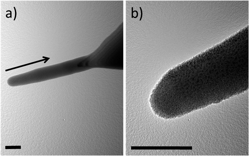 | ||
| Fig. 6 TEM images of a nanoneedle coated with DLC film. The film is 7 nm thick on the apex and ∼3 nm on the sides of the nanoneedle. The arrow shows the direction of deposition. Scale bar is 100 nm. | ||
3.4 Internal stress
One of the factors seriously limiting tribological applications of DLC films is their large internal stress (up to 10 GPa). It can be caused by a mismatch between thermal coefficients of DLC and the substrate. However, even when the deposition process does not involve any significant heating, there is still an intrinsic stress. This stress is believed to arise in the process of deposition as some of the incoming energetic C ions penetrate the already deposited DLC layer causing subsurface growth that creates a significant compressive stress in the film.2,42 The magnitude of the stress can be related to the microstructure of the deposited DLC layer and depends on deposition parameters, in particular on the kinetic energy of ions striking the DLC surface during deposition. For continuous films (i.e. when they are thick enough for the coalescence of independently growing islands to occur) the average macroscopic stress in DLC is independent of the film thickness.43 It is known that the internal stress of DLC can be reduced by alloying it with a variety of chemical elements (e.g. with Si, B, Ti, Cr, Al etc.38). However, such doping often deteriorates the mechanical properties of the coating, reducing its hardness and elastic modulus.44To determine the magnitude of residual stress we employed the previously used method based on measurements of deformation of flexible film–substrate structures.28 For this purpose a number of AFM probes having different stiffness were coated with DLC films. For tapping mode probes, having comparatively thick (∼4 μm) silicon cantilevers, coating with DLC films of 5–20 nm thick did not induce any noticeable deformation. However, for much softer, contact mode probes, with significantly thinner (0.4–0.5 μm) silicon nitride cantilevers, the deposited DLC films caused significant bending, as shown in Fig. 7. The direction of bending indicates that the DLC films expand during fabrication. The magnitude of stress can be deduced from the Stoney's formula:45
 | (3) |
 | ||
| Fig. 7 (a) Five silicon nitride AFM cantilevers on the same chip (MSNL, Bruker) bent after coating them with a 9 nm thick DLC film. (b) Two silicon nitride cantilevers (Budget sensors) after coating them with a 43 nm thick DLC film. Scale bar is 100 μm. | ||
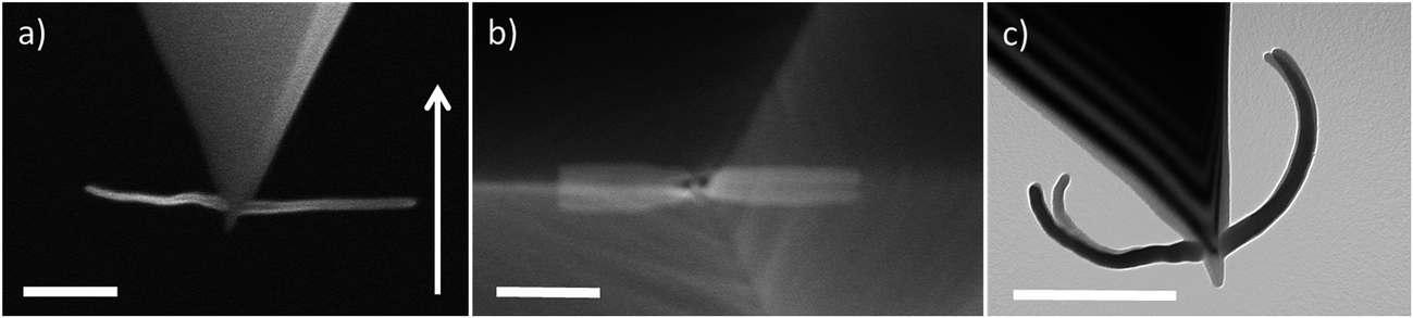
The problem of internal stress becomes even more important when DLC is used for coating of thinner structures. As the ratio of the thickness of the DLC layer to the thickness of the substrate increases, it becomes increasingly difficult to avoid deformation of the sample after coating. We investigated this by coating free-standing nanostructures grown using the EBID method. The EBID technique allows the growth of structures of different shapes and is widely used in nanofabrication. Our earlier studies of mechanical properties of EBID-grown blades47 and needles48 showed that they are extraordinary flexible, capable of undergoing large deflections without inelastic deformation. The material deposited by the EBID method is mostly composed of amorphous carbon but has a comparatively low elastic modulus of ∼28 GPa (ref. 47) and so traditionally it is not included into the DLC family. Coating of such structures with a DLC film is expected to make them harder and increase their wear resistances. However, they are prone to strain-induced deformations and we have found that the coating must be symmetrical to balance forces produced by stress. As shown in Fig. 6, a cylindrical structure (nanoneedle) of 90 nm in diameter stays straight after a symmetric coating from the sharp side with a nominally 7 nm-thick DLC film.
Fig. 8 shows the other extreme, when the deposition of a 10 nm-thick DLC layer was performed only on the top side of two amorphous-carbon ‘blades’ (strictly, speaking, each of the blades was composed of two fingers, which, as can be seen in Fig. 8c, were deformed slightly differently). Eqn (3) can be used to estimate the internal stress in this case too. Using Es = 28 GPa and measuring the radius of curvature R of the deformed blade from the electron microscopy image we estimated the internal stress in this case to be 0.6–0.8 GPa, which is close to the stress observed for AFM coated probes.
 | ||
| Fig. 8 DLC coating causes bending of amorphous-carbon blades grown on an AFM tip: (a and b) side and top view before deposition; (c) side view after deposition of a 10 nm thick DLC film. The arrow in (a) shows the direction of deposition. Scale bar is 500 nm. | ||
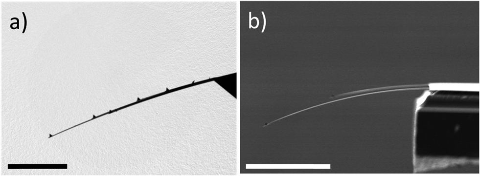
Fig. 9 shows another example, where the deposition was only slightly asymmetric. The direction of deposition was approximately at 7° to the axis of symmetry of the structure, which has the shape of a hand with 6 fingers. The deposition caused complex deformation of the “fingers”, turning the structure into something which looks like a begging (or beckoning) hand.
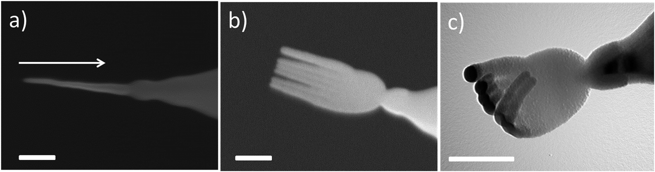 | ||
| Fig. 9 Even small asymmetry in the DLC coating may cause complex deformation of carbon nanostructures. A hand-like amorphous-carbon nanostructure grown on an AFM tip: (a and b) side and top view before deposition; (c) after deposition of a 10 nm DLC film. The arrow in (a) shows the direction of deposition. Scale bar is 200 nm. | ||
3.5 Mechanical properties of coatings
The scans were performed in the regime of constant load force of 1 μN, which was controlled by tracking the cantilever deflection. This force is significantly larger than the tip-sample adhesion force (<30 nN), so any variations in the adhesion during scans could be neglected. The wear volume was calculated from comparison of TEM images before and after the test.
During scans, information about topography of the scanned area was collected. It is known that AFM topographical images are a product of convolution of the tip shape and real topography of the sample and the shape of the AFM probe apex can be evaluated from these images.51 This gives a simple means of monitoring all changes in the AFM probe shape during the wear tests. In all our experiments we observed a gradual change in the probes' shape, indicating that there were no significant fractures of the probes or any coating failures.
Fig. 10 shows TEM images of three probes taken after sliding the same distance (4 mm) on SiO2. The first probe (a) was uncoated, the second (b) coated with a 60 nm film of DLC and the third (c) first coated with a 60 nm layer of DLC and then etched by Ar plasma to remove ∼70% of the coating. From the tip images obtained in a TEM before and after the test, we estimated the wear rates to be 4.8 × 10⁻¹³ m2 N−1 for the uncoated probe, 3.8 × 10⁻¹⁵ m2 N−1 for the coated probe and 1.8 × 10⁻¹⁵ m2 N−1 for the coated and then Ar etched probe. These numbers show that DLC coating strongly (by more than two orders of magnitude) decreases the wear rate of silicon probes. It is interesting that Ar etching increases wear resistance even further. Ion bombardment of DLC films is known to change the hydrogen content and the hybridisation state of carbon. In particular, it can increase the concentration of sp3 bonds thus increasing hardness of the DLC film,52 which in turn improves wear resistance.
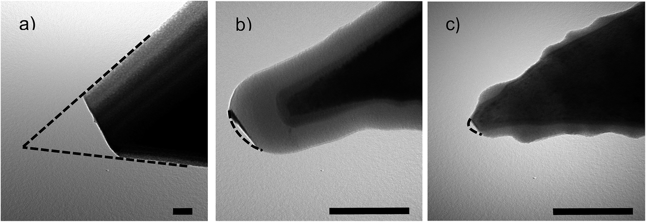 | ||
| Fig. 10 TEM images of AFM tips after wear test: (a) uncoated, (b) DLC coated and (c) DLC coated and Ar ion etched. Dashed lines show the original shape of the tips. Scale bar is 100 nm. | ||
The first mode resonant frequency of an uncoated cantilever is given by the following relation:56
 | (4) |
 | (5a) |
 | (5b) |
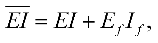
The individual moments of inertia of each of the two ‘layers’ are described, respectively, by 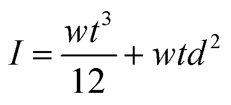 and
and 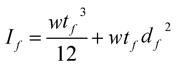 , where d and df are the distances between the centroidal axis of the coated cantilever and the neutral axes of each of the ‘layers’. Then for the ratio of the resonant frequencies with, f, and without, f0, the DLC film the following relation is valid:
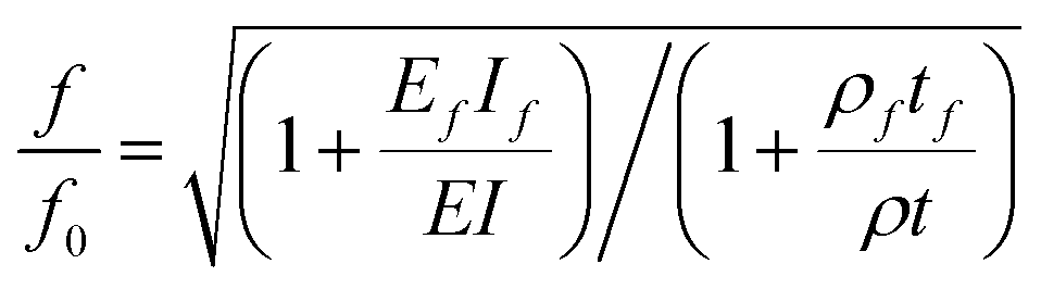 | (6) |
This equation can be solved numerically to extract the Young's modulus of the film if the resonant frequencies before and after the coating are known. For the case of ultrathin films an approximate analytical solution can be obtained:
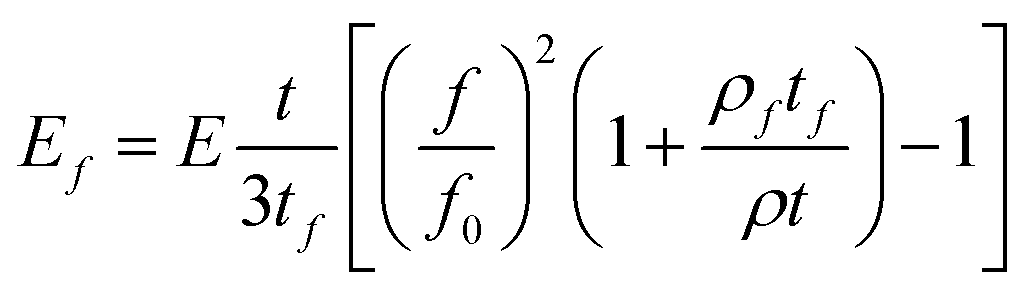 | (7) |
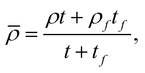
In our experiments we used AFM probes with comparatively thick (2–4 μm) cantilevers to avoid any bending them after coating with DLC films. To measure the cantilever's resonant frequency, an AFM probe was mounted within the piezo-holder of the AFM microscope and the standard auto-tuning procedure was activated. This induced frequency sweeps in the range of 100–500 kHz during which the resonance peak was determined. It was found that coating of the AFM probes with a 24 nm DLC film causes an increase in the resonant frequency (∼180 kHz) by ∼1.5%. Using 169 GPa (ref. 58) and 2.3 g cm−3 as the elastic modulus and density of silicon and 2.2 g cm−3 as the density of DLC39 the Young's modulus of the deposited ultrathin coatings was determined to be in the range of 185–209 GPa.
4. Conclusions
In this paper, comprehensive studies of structural and mechanical properties of DLC films produced by an MEPCVD method have been performed. It was found that ultrathin (5–20 nm) films of this material are very smooth with ultralow intrinsic roughness. In the case of coating of high-aspect-ratio structures, roughness is minimal on the side which is normal to the deposition direction. Coating usually increased the radius of curvature of sharp features, such as the AFM probe tip apex but in some conditions this increase can be very small. Sharpening with Ar etching increases the roughness of the DLC coating. The DLC films are stressed, which may cause mechanical deformation of flexible nanostructures, if they are coated asymmetrically. However, the stress (0.4–0.6 GPa) is lower than the typical values for DLC films obtained by other methods. Following the traditional classification of DLC,38,39 this material corresponds to hydrogenated tetrahedral amorphous carbon films (ta-C:H) that have a low hydrogen content (22–26%), large sp3 content (54–56%) and large, for hydrogenated carbons, elastic modulus (∼200 GPa). All these properties make this material a good candidate for protective coating of nanostructures. In particular, we have demonstrated that coating of silicon AFM probes improves their wear resistance by more than 100 times. However, the significant internal stress of ultrathin DLC films can be a serious obstacle for certain nanoscale applications.Acknowledgements
The authors gratefully thank the Bath Ventures for financial support (SPARK award) of this work. JDB and SNG thank D. Sutton for useful discussions.References
- S. Aisenberg and R. Chabot, J. Appl. Phys., 1971, 42, 2953–2958 CrossRef CAS PubMed
.
- Y. Lifshitz, S. R. Kasi and J. W. Rabalais, Phys. Rev. Lett., 1989, 62, 1290–1293 CrossRef CAS
- D. R. McKenzie, Rep. Prog. Phys., 1996, 59, 1611–1664 CrossRef CAS
- M. C. Salvadori, M. C. Fritz, C. Carraro, R. Maboudian, O. R. Monteiro and I. G. Brown, Diamond Relat. Mater., 2001, 10, 2190–2194 CrossRef CAS
- N. Savvides, J. Appl. Phys., 1984, 55, 4232–4238 CrossRef CAS PubMed
- F. Davanloo, E. M. Juengerman, D. R. Jander, T. J. Lee and C. B. Collins, J. Appl. Phys., 1990, 67, 2081–2087 CrossRef CAS PubMed
- L. Holland and S. M. Ojha, Thin Solid Films, 1976, 38, L17–L19 CrossRef CAS
- M. Weiler, K. Lang, E. Li and J. Robertson, Appl. Phys. Lett., 1998, 72, 1314–1316 CrossRef CAS PubMed
- C. Jaoul, O. Jarry, P. Tristant, T. Merle-Mejean, M. Colas, C. Dublanche-Tixier and J. M. Jacquet, Thin Solid Films, 2009, 518, 1475–1479 CrossRef CAS PubMed
- J. C. Damasceno, S. S. Camargo and M. Cremona, Thin Solid Films, 2003, 433, 199–204 CrossRef CAS
- J. Robertson, Thin Solid Films, 2001, 383, 81–88 CrossRef CAS
- A. C. Ferrari, Surf. Coat. Technol., 2004, 180, 190–206 CrossRef PubMed
- J. A. McLaughlin and P. D. Maguire, Diamond Relat. Mater., 2008, 17, 873–877 CrossRef CAS PubMed
- A. Grill, Diamond Relat. Mater., 2003, 12, 166–170 CrossRef CAS
- G. Dearnaley and J. H. Arps, Surf. Coat. Technol., 2005, 200, 2518–2524 CrossRef CAS PubMed
- F. M. Wang, M. W. Chen and Q. B. Lai, Thin Solid Films, 2010, 518, 3332–3336 CrossRef CAS PubMed
- B. Bhushan, in Tribology of Diamong-Like Carbon Films. Fundamentals and Applications, ed. C. Donnet and A. Erdemir, Springer Science, New York, 2008, pp. 510–570 Search PubMed
- P. R. Goglia, J. Berkowitz, J. Hoehn, A. Xidis and L. Stover, Diamond Relat. Mater., 2001, 10, 271–277 CrossRef CAS
- J. D. Beard, D. J. Burbridge, A. V. Moskalenko, O. Dudko, P. L. Yarova, S. V. Smirnov and S. N. Gordeev, Nanotechnology, 2009, 20, 445302 CrossRef CAS PubMed
- W. Shim, A. B. Braunschweig, X. Liao, J. N. Chai, J. K. Lim, G. F. Zheng and C. A. Mirkin, Nature, 2011, 469, 516–521 CrossRef CAS PubMed
- A. A. Tseng, Small, 2011, 7, 3409–3427 CrossRef CAS PubMed
- A. H. Tan, Diamond Relat. Mater., 2007, 16, 467–472 CrossRef CAS PubMed
- F. X. Liu and Z. L. Wang, Surf. Coat. Technol., 2009, 203, 1829–1832 CrossRef CAS PubMed
- N. Soin, S. S. Roy, S. C. Ray, P. Lemoine, M. A. Rahman, P. D. Maguire, S. K. Mitra and J. A. McLaughlin, Thin Solid Films, 2012, 520, 2909–2915 CrossRef CAS PubMed
- D. P. Liu, G. Benstetter, E. Lodermeier, X. Chen, J. N. Ding, Y. H. Liu, J. L. Zhang and T. C. Ma, Diamond Relat. Mater., 2003, 12, 1594–1600 CrossRef CAS
- L. Q. Gou, X. L. Shi, X. M. Zhao, Y. Bai and L. J. Qiao, Surf. Coat. Technol., 2012, 206, 4099–4105 CrossRef CAS PubMed
- J. Robertson, in Tribology of Diamong-Like Carbon Films. Fundamentals and Applications, ed. C. Donnet and A. Erdemir, Springer Science, New York, 2008, pp. 13–24 Search PubMed
- P. Lemoine, J. F. Zhao, A. Bell, P. Maguire and J. McLaughlin, Diamond Relat. Mater., 2001, 10, 94–98 CrossRef CAS
- Y. Pauleau, in Tribology of Diamong-Like Carbon Films. Fundamentals and Applications, ed. C. Donnet and A. Erdemir, Springer Science, New York, 2008, pp. 102–138 Search PubMed
- T. Zaharia, P. Kudlacek, M. Creatore, R. Groenen, P. Persoone and M. C. M. van de Sanden, Diamond Relat. Mater., 2011, 20, 1266–1272 CrossRef CAS PubMed
- P. Sander, U. Kaiser, M. Altebockwinkel, L. Wiedmann, A. Benninghoven, R. E. Sah and P. Koidl, J. Vac. Sci. Technol., A, 1987, 5, 1470–1473 CAS
- S. R. P. Silva, K. J. Clay, S. P. Speakman and G. A. J. Amaratunga, Diamond Relat. Mater., 1995, 4, 977–983 CrossRef CAS
- Z. Sun, X. Shi and E. Liu, Thin Solid Films, 1999, 355, 146–150 CrossRef
- S. Aleksandrov, Method and apparatus for forming diamond-like coatings, US Pat. 0178436, 15 July 2010
- I. Horcas, R. Fernandez, J. M. Gomez-Rodriguez, J. Colchero, J. Gomez-Herrero and A. M. Baro, Rev. Sci. Instrum., 2007, 78, 013705 CrossRef CAS PubMed
- P. Klapetek, D. Necas and C. Anderson, Free Software Foundation, Inc, 2002
- W. Ding, D. A. Dikin, X. Chen, R. D. Piner, R. S. Ruoff, E. Zussman, X. Wang and X. Li, J. Appl. Phys., 2005, 98, 014905 CrossRef PubMed
- J. Robertson, in Tribology of Diamong-Like Carbon Films. Fundamentals and Applications, ed. C. Donnet and A. Erdemir, Springer Science, New York, 2008, pp. 139–154 Search PubMed
- A. C. Ferrari, in Tribology of Diamong-Like Carbon Films. Fundamentals and Applications, ed. C. Donnet and A. Erdemir, Springer Science, New York, 2008, pp. 25–82 Search PubMed
- W. G. Cui, Q. B. Lai, L. Zhang and F. M. Wang, Surf. Coat. Technol., 2010, 205, 1995–1999 CrossRef CAS PubMed
- M. C. Salvadori, D. R. Martins and M. Cattani, Surf. Coat. Technol., 2006, 200, 5119–5122 CrossRef CAS PubMed
- J. Robertson, Diamond Relat. Mater., 1994, 3, 361–368 CrossRef CAS
- Y. Pauleau, in Tribology of Diamong-Like Carbon Films. Fundamentals and Applications, ed. C. Donnet and A. Erdemir, Springer Science, New York, 2008, pp. 102–138 Search PubMed
- A. Bendavid, P. J. Martin, C. Comte, E. W. Preston, A. J. Haq, F. S. M. Ismail and R. K. Singh, Diamond Relat. Mater., 2007, 16, 1616–1622 CrossRef CAS PubMed
- G. G. Stoney, Proc. R. Soc. London, Ser. A, 1909, 82, 172–175 CrossRef CAS
- A. Khan, J. Philip and P. Hess, J. Appl. Phys., 2004, 95, 1667–1672 CrossRef CAS PubMed
- J. D. Beard and S. N. Gordeev, Nanotechnology, 2010, 21, 475702 CrossRef CAS PubMed
- J. D. Beard and S. N. Gordeev, Nanotechnology, 2011, 22, 174303 CrossRef PubMed
- H. Bhaskaran, B. Gotsmann, A. Sebastian, U. Drechsler, M. A. Lantz, M. Despont, P. Jaroenapibal, R. W. Carpick, Y. Chen and K. Sridharan, Nat. Nanotechnol., 2010, 5, 181–185 CrossRef CAS PubMed
- J. F. Archard, J. Appl. Phys., 1953, 24, 981–988 CrossRef PubMed
- J. Vesenka, R. Miller and E. Henderson, Rev. Sci. Instrum., 1994, 65, 2249–2251 CrossRef CAS PubMed
- C. Heau, in Tribology of Diamong-Like Carbon Films. Fundamentals and Applications, ed. C. Donnet and A. Erdemir, Springer Science, New York, 2008, pp. 469–483 Search PubMed
- P. Lemoine, J. P. Quinn, P. D. Maguire and J. A. McLaughlin, in Tribology of Diamong-Like Carbon Films. Fundamentals and Applications, ed. C. Donnet and A. Erdemir, Springer Science, New York, 2008, pp. 83–101 Search PubMed
- R. Pastorelli, A. C. Ferrari, M. G. Beghi, C. E. Bottani and J. Robertson, Diamond Relat. Mater., 2000, 9, 825–830 CrossRef CAS
- C. R. Stoldt, M. C. Fritz, C. Carraro and R. Maboudian, Appl. Phys. Lett., 2001, 79, 347–349 CrossRef CAS PubMed
- I. R. Voiculescu, M. E. Zaghloul, R. A. McGill and J. F. Vignola, Proc. Inst. Mech. Eng., Part C, 2006, 220, 1601–1608 CrossRef CAS
- T. Kocourek, M. Ruzek, M. Landa, M. Jelinek, J. Miksovsky and J. Kopecek, Surf. Coat. Technol., 2011, 205, S67–S70 CrossRef CAS PubMed
- M. A. Hopcroft, W. D. Nix and T. W. Kenny, J. Microelectromech. Syst., 2010, 19, 229–238 CrossRef CAS
Footnote |
| † Current address: College of Engineering, University of Exeter, North Park Road, Exeter, EX4 4QF, UK. |
| This journal is © The Royal Society of Chemistry 2014 |