DOI:
10.1039/C4RA02791D
(Paper)
RSC Adv., 2014,
4, 33184-33189
Electronic impurities (Fe, Mn) doping in CdSe nanostructures for improvements in photoelectrochemical applications
Received
29th March 2014
, Accepted 27th June 2014
First published on 27th June 2014
Abstract
CdSe nanostructures (NSs) were tuned using different dopants (Fe:CdSe and Mn:CdSe) on electro-synthesized photoelectrochemical cells with fluorine-doped tin oxide (FTO) coated glass and stainless steel substrates. Thin films were characterized for their structural, morphological, and photoelectrochemical characteristics. Their optical and semiconducting parameters were also analyzed to determine the suitability of these films for photoelectrochemical (PEC)/solar cell applications. X-ray diffraction (XRD) analysis revealed that the films are polycrystalline in nature and suitable for improved solar cell applications. Scanning electron microscopy (SEM) studies illustrated that the thin films were adhered to the substrate uniformly and dopants were involved in the formation of novel nanostructured composition. Optical studies showed that the films are of direct band gap. For all the films, the semiconductor parameter values were in the better range of other transition metal chalcogenides, confirming that undoped CdSe and Fe:CdSe, Mn:CdSe thin films are capable as solar/PEC cell materials.
1. Introduction
Electronic impurity doping is a method in which impurity atoms are deliberately supplemented in bulk semiconductors to provide either additional electrons (n-type doping) or additional holes (p-type doping). These carriers then enable electrical transport through an otherwise poorly conducting material.1 These materials also exhibit size dependent optical properties, which can be useful in solar cells2 and solid-state lighting.3 For these applications, electrical current must be collected or injected from nanocrystal thin films. Because thin films are inherently insulating, the introduction of extra carriers significantly enhances the conductivity. CdSe materials, including placement of electron-donating molecules in the vicinity of the nanocrystals surface (remote doping)4 and the application of electrochemical doping5 are poorly understood. It has been previously reported that when carriers interacted, conductivity was dramatically increased.5 Semiconductor nanostructures have been widely discussed by several research groups as an important class of functional materials with potential applications in solid-state lighting,6–8 lasers,9 and photovoltaics.10,11 In particular, we postulate that providing extra carriers to CdSe nanocrystals using “impurity doping” system can be possible. In the present study, we prove that CdSe materials appear to be the most suitable for facile processing and have good chemical stability, with tenability of their physical properties achieved through particle-size control.
On the incorporation of iron, manganese in II–VI semiconductors as isovalent doping systems, no additional charge was introduced by the impurity, which led to the formation of new radiative recombination centres. An important step forward would be the controlled doping of nanostructures (NSs) with impurities capable of affecting the electric and/or optical properties of the currently developed system. Analogous with the p-doping and n-doping of bulk semiconductors, the permanent incorporation of active charges into NSs could be achieved by the inserting ions of transition metals with a variable valence as substitutional or interstitial defects.12 In this case, the impurities introduce atomic-like states within the forbidden gap of the host semiconductor that can exchange charges with the valence and conduction bands via radiative and nonradioactive transitions. Similar approach for the improvement of electronic doping and the incorporation of transition metals, such as Fe, Mn, into NSs having various compositions has been reported.13
CdSe thin films have been prepared in the past by several techniques such as chemical bath and pulsed laser deposition,14,15 electrochemical deposition,16 vacuum evaporation technique17 and pulsed laser method.18 CdTe thin films have been deposited by various deposition methods such as pulsed laser deposition,19 spray deposition,20 co-evaporation,21 vacuum evaporated,22 etc. Murase et al. used Te doped CdSe thin film for photoluminescence applications and concluded that the spectral width of the doped material is equal to that of the undoped sample. However, emission from the doped material undergoes a large blue shift during successive measurements. This is attributed to the instability of the Te dopant with a larger ionic size in nanocrystals.23 Wang et al.24 investigated the synthesis of Mn-doped ZnS thin film and its optical properties. Alsaad et al.25 studied the structural, electronic and magnetic properties of Fe, Co, Mn doped GaN and Mn doped ZnO sample.
In the present work, we have attempted, for the first time, the study of the structural, optical and electrical properties of CdSe thin films tuned by electronic doping systems designed with transition metal ions (Fe, Mn). We report the electrochemical synthesis of CdSe nanostructures and their possible tuning in a comprehensive manner to understand the mechanism and possible applications. Furthermore, improved CdSe materials using different (Fe, Mn) dopants were characterized by structural, morphological and photoelectrochemical properties. Current research efforts offer a novel system and improved CdSe composites for the establishment of binary materials by potentiostatic mode for the construction of solar cells.
2. Experimental details
Electrodeposition was carried out using a classical three-electrode potentiostatic mode system with a saturated calomel electrode (SCE) as the reference electrode and a graphite plate (20 × 40 × 5 mm3) as the counter electrode. Stainless steel and fluorine-doped tin oxide (FTO) coated glass substrates were used as working electrode. Stainless steel substrates were polished by smooth (zero fine grades) polish paper prior to electrodeposition. To remove the oily substance from the surface, cleaned substrates were etched in 10% H2SO4 for 2 min, and finally ultrasonically cleaned with double distilled water. FTO coated glass substrates were boiled in chromic acid for 15 min, ultrasonically cleaned with double distilled water and then dried with hot air. The electrodeposition was carried out on unit area (1 × 1 cm2) of the substrates in potentiostatic mode in a electrolytic bath containing 0.75 M CdSO4·8H2O (47 ml), 0.07 M SeO2 (50 ml) and 0.75 M FeSO4 (3 ml), 0.75 M MnSO4 (3 ml) and ethylenediaminetetraacetic acid (EDTA) tetra sodium salt (2 ml) as a complexing agent. The deposition time and percentage of doping were optimized using photoelectrochemical technique. After film deposition, the films were rinsed in double distilled water and used for further investigations.
The films were characterized for their structural properties by using a Philips X-ray diffractometer PW-3710 (λ = 1.54 Å) for copper (Cu-Kα) at 20–100° range. The surface morphology of the film was investigated by field emission scanning electron microscopy (FE-SEM) using JEOL JSM-6360. Optical absorption of the films deposited on FTO coated glass (FTO) substrate was carried out in the wavelength range of 350–950 nm using Systronic model-119 spectrophotometer. To study the interaction between liquid and thin film surface contact angle measurement was carried out by Rame-Hart USA equipment equipped with a CCD camera. PEC solar cell was fabricated using a two-electrode configuration comprising n-CdSe and Fe:CdSe, Mn:CdSe thin films as a photoanode, graphite as a counter electrode. The redox electrolyte was 1 M polysulphide (NaOH:Na2S:S). The cell was illuminated with a 100 W tungsten filament lamp (intensity 30 mW cm−2) for measuring short circuit current (Isc) and open circuit voltage (Voc).
3. Results and discussion
3.1 XRD studies
Fig. 1 demonstrates the X-ray diffraction (XRD) pattern obtained for CdSe films prepared by the electrodeposition method for different dopant Fe, Mn for 3%. Fig. 1 reveals that the deposited films exhibits hexagonal structure.16 The observed values of lattice constants are found to be ±0.03 different from the standard values. The observed diffraction peaks of hexagonal CdSe are at 2θ values of angles 25.13°, 25.84°, 29.56°, 42.98°, 50.34°, 60.71°, 74.33°, 81.19° and 90.56° degree corresponding to the lattice planes of (002), (110), (201), (203), (300), (302) and (220), respectively. All the peak intensities identified are from CdSe and no additional lines matching to Cd, CdO, SeO2 and Se are observed in Fig. 1a. As shown in Fig. 1b and c, no additional peaks of Fe, Mn are present. The height of the (200) plane is found to be higher than all the other peaks in the diffractograms (Fig. 1a–c) showing that the crystallites are preferentially oriented along (200) plane. This result strongly suggests that the potentiostatic mode of electrodeposition method is suitable for the preparation of single phase hexagonal CdSe films. The ‘d’ values observed in the present work are found to be in good agreement with the JCPDS file for hexagonal CdSe.26
 |
| | Fig. 1 XRD pattern of the potentiostatically deposited (a) pure CdSe, (b) 3% Fe:CdSe (c) 3% Mn:CdSe thin films on the stainless steel substrates. | |
The average crystallite size was calculated using the well-known Scherer's relation (1)
| |
 | (1) |
where
D is the crystallite size,
β is the broadening of diffraction line measured at the half of its maximum intensity (rad) (FWHM) and
λ is the X-ray wavelength (0.15406 nm). The decrease in crystallite size may be attributed to a higher nucleation rate compared to the growth rate.
3.2 Surface morphological studies
The surface morphology of the electrodeposited potentiostatic mode CdSe thin film and 3% Fe:CdSe, 3% Mn:CdSe doping was investigated by a scanning electron micrograph. Fig. 2a–c shows the SEM image of CdSe thin film and 3% Fe:CdSe, 3% Mn:CdSe thin film. The SEM micrographs show a covering of nanoseed and nanofiber-like morphology over the entire substrate. This could be attributed to the fact that the deposited CdSe thin films were processed with different dopants such as Fe, Mn, which led to the formation of innovative nanostructures such as nanoseeds-like and horns-like small spheres morphologies over the entire substrate with grain size of about 100 nm, 190 nm, respectively. Fig. 2a shows interconnected nanoseeds that are very useful for the transformation of ions in electrolyte. Fig. 2b shows the interrelated nanohorns, which are found to be very constructive for the conversion of ions in electrolyte. Fig. 2c shows the consistent nanosemisphere, which is very beneficial for the renovation of electrons in liquid electrolyte, and is very advantageous for the exchange of electron-hole pair in electrolytic bath. All the SEM nanostructures show the ion in between nanoseeds and nanosemispheres with the porous structure of the sample going deep inside the surface (Fig. 2a–c). In brief, all the nanostructures change into highly porous morphology with interconnected networks, which are found to be highly feasible for solar cell applications (discussed later). We strongly believe that the development of nanostructures, nanohorns and nanospheres is successfully accomplished by the ionic doping system. The formation of specialized nanostructures was possible because of the relatively slow electrodepositing growth of nanocrystals at ambient temperature. Perhaps, the initial nucleation centers were locked on substrates, which do not allow the growth by other routes and only allow the extension of initially grown materials thus the formation of large crystal at primary phase and then nanowires with a range of orientations.
 |
| | Fig. 2 SEM images of potentiostatically deposited (a) pure CdSe, (b) 3% Fe:CdSe (c) 3% Mn:CdSe thin films on the stainless steel substrates. | |
3.3 Optical studies
The optical absorption study of the as-deposited nanocrystalline CdSe and 3% Fe:CdSe, 3% Mn:CdSe thin films was carried out using a UV-Vis-IR spectrophotometer in the wavelength range 350 to 900 nm. Fig. 3 shows the absorbance versus wavelength of pure CdSe and 3% Fe, 3% Mn doped CdSe thin films. Fig. 3 shows a plot of (αhν)2 versus (hν) which is linear at the absorption edge, confirming that the material has a direct band gap. The absorption data were analyzed using the classical relation for near edge optical absorption of semiconductors,| |
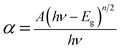 | (2) |
where A is a constant, Eg is the band gap, n is a constant equal to one for direct gap semiconductors and four for indirect gap semiconductor materials. The variation of optical absorbance with wavelength shows that CdSe and 3% Fe, 3% Mn doped CdSe thin films are semiconducting material with a direct band gap.
 |
| | Fig. 3 Absorbance spectra and the plots of the band gaps of potentiostatically deposited (a) pure CdSe, (b) 3% Fe:CdSe (c) 3% Mn:CdSe thin film on the FTO coated glass substrates. | |
Fig. 3 shows that the optical studies of different dopant on CdSe thin film. Fig. 3 shows the effect of different dopants on band gap. Fig. 3a and b shows that the band gap values are found to be 1.89 eV for CdSe, 1.69 eV for CdSe:Mn and 1.60 eV for CdSe:Fe thin films. It is observed that there is slight decrease in band gap for CdSe:Mn and CdSe:Fe thin films. This decrease may be because of the improvement of the grain structure of the films, which may be because of the segregation of impurity atoms along the grain boundaries.27 The band gap value of CdSe and CdSe:Fe thin films obtained in this work is found to be in close agreement with the previously reported values.28 Fig. 3a–c shows that the band gap energies of CdSe and Fe:CdSe, Mn:CdSe thin films are the most attractive and significant. The size-tunable emission, lasing capabilities and other photophysical properties that have attracted attention to colloidal undoped semiconductor CdSe can be retained, while the Mn2+ impurities introduce an additional degree of freedom for controlling these physical properties.29
3.4 Wettability test
Wettability involves the interaction between the polysulfide electrolyte and undoped in contact CdSe, 3% Fe:CdSe, 3% Mn:CdSe, which is characterized by the value of the measured contact angle. Highly water repellent surfaces can be achieved by low surface energy coatings combined with specially designed surface textures.30–32 In the present case, the contact angle measurement has been used to study the quality of pure CdSe and the effects of different dopant (3% Fe:CdSe, 3% Mn:CdSe) thin films to be used in photoelectrochemical solar cell. Fig. 4 shows the images of water contact angle measurements on CdSe and different dopants. From the obtained values, the water contact angle measurement decreased systematically as the surface roughness increased. When different doping metals, such as Fe and Mn, were used, the contact angle decreases from 66° to 30°,33 which may be because of the strong cohesive force between the water droplet and hydrous content in CdSe films and different doping films. This specific property is useful for enabling intimate contact of aqueous electrolyte. We believe that this specific property will tentatively demonstrate the feasibility of Mn, Fe:CdSe film surface in the electrolyte/electrode boundary for enhanced performances.34
 |
| | Fig. 4 Variation of water contact angles of CdSe thin films with different dopants (Fe, Mn). | |
3.5 Photoelectrochemical (PEC) solar cell study
The working attitude of CdSe, Mn:CdSe and Fe:CdSe electrode is shown in Fig. 5. Here, we have represented an imaginative view of the electron–hole regeneration, moving and its production of CdSe and Mn:CdSe, Fe:CdSe photoelectrodes in a photoelectrochemical cell. The CdSe and Mn:CdSe, Fe:CdSe samples are the working photoanode electrode and graphite acts as a counter electrode. The aqueous 1 M polysulfide electrolyte was added via pre-drilled holes, which act as redox couple and then sealed with a sealant. When this device is illuminated under light, the following reaction occurs step by step. The process of electron injection commences when a photon of energy is absorbed by the CdSe, Mn and Fe:CdSe electrodes in the visible region to create an electron–hole pair. The mechanism of visible light-assisted photoexcitation in CdSe, Mn:CdSe and Fe:CdSe photoanode followed by charge transport can be summarized by the following equations. When the photons are absorbed by CdSe, Mn:CdSe and Fe:CdSe, the electron–hole pairs are generated as:| | |
CdSe(hν)photonenergy → CdSe (h+ + e−)
| (3) |
 |
| | Fig. 5 Schematic device fabrication of photoelectrochemical cell. | |
When the electron–hole is separated, the electrons are instantaneously transferred to the conduction band (CB) due to suitable conduction band-offsets. Finally, the electrons are collected by the FTO substrate and subsequently flow to an external circuit, which is shown in Fig. 5.
The light energy harvesting aspects of nanostructures (NSs) and nanosemisphere (NSSs) were evaluated using a liquid junction photoelectrochemical cell with undoped CdSe and 3% Fe:CdSe and 3% Mn:CdSe films as the photoanode films under light illumination of 30 mW cm−2. The counter electrode was graphite and the electrolyte consisted of 1 M polysulfide electrolyte (Na2S:S:NaOH) in deionizer H2O. The J–V characteristics of the NSs and NSSs employing three different photoanodes CdSe NSs, 3% Fe:CdSe NSs, and 3% Mn:CdSe NSs films deposited via the potentiostatic mode of electrodeposition technique on FTO coated glass substrates are presented in Fig. 6. The typical active area of the unmasked photoanode was 0.5 cm2. The short-circuit current density (JSC), open-circuit voltage (VOC), fill factor (FF) and overall conversion efficiency (η) of CdSe NSs and Fe:CdSe, Mn:CdSe are summarized in Table 1. As shown in Fig. 6, the short-circuit current density (Jsc), open-circuit potential (Voc), fill factor (FF), and conversion efficiency (η) of undoped CdSe and Fe:CdSe sensitized cells are 520 μA cm−2, 0.7 V, 0.42, and 0.49% and 1.27 mA cm−2, 780 mV, 0.84 and 2.64%, respectively. The higher efficiency of Fe:CdSe is attributed to its broader light absorption range than that of he undoped CdSe, and the lower FF of CdSe-electrode is because of a low driving force for electron injection.35,36 When both the electrodes are combined sequentially in a co-sensitized structure, synergistic improvement in Jsc and Voc is observed along with a slight change in FF (0.84), which leads to a high conversion efficiency of 2.61%. Fig. 7 shows the dependence of solar cell parameters CdSe on the doping of Fe and Mn the short-circuit current (Jsc (black line)), open-circuit voltage (Voc (blue line)), fill factor (FF) and overall power conversion efficiency (η) under light illumination of 30 mW cm−2.
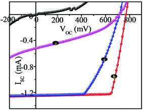 |
| | Fig. 6 J–V characteristics of pure CdSe and 3% Fe:CdSe, 3% Mn–CdSe thin films in dark and under light illumination. | |
Table 1 Photoelectrochemical cell performance of pure and doped CdSe
| Sr. no |
Deposited film |
Isc (mA) |
Voc (mV) |
Fill factor |
Efficiency (in %) |
| 1 |
Pure-CdSe |
0.520 |
700 |
0.42 |
0.49 |
| 2 |
3% Fe–CdSe |
1.27 |
780 |
0.84 |
2.64 |
| 3 |
3% Mn–CdSe |
1.21 |
710 |
0.56 |
1.60 |
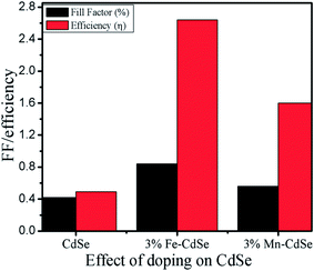 |
| | Fig. 7 Dependence of solar cell parameters CdSe on the doping of Fe and Mn short-circuit current (Jsc (black line)), open-circuit voltage (Voc (blue line)), fill factor (FF), and overall power conversion efficiency (η) under light illumination of 30 mW cm−2. | |
4. Conclusions
In summary, an undoped CdSe, 3% Fe:CdSe and 3% Mn:CdSe films as a photoanode for photoelectrochemical cell has been prepared by using a simple, rapid and effective electrodeposition (ED) technique. This technique can synthesize undoped CdSe, 3% Fe:CdSe and 3% Mn:CdSe quickly suppress their surface defects as well as form a good contact between the liquid electrolyte and the CdSe, 3% Fe:CdSe, and 3% Mn:CdSe electrodes. These results imply that electrodeposition was facile and suitable for different dopant materials for miscellaneous applications.
References
- A. Sahu, M. S. Kang, A. Kompch, C. Notthoff, A. W. Wills, D. Deng, M. Winterer, C. D. Frisbie and D. J. Nor, Nano Lett., 2012, 12, 2587 CrossRef CAS.
- I. Gur, N. A. Fromer, M. L. Geier and A. P. Alivisatos, Science, 2005, 310, 462 CrossRef CAS PubMed.
- S. Coe, W. K. Woo, M. Bawendi and V. Bulovic, Nature, 2002, 420, 800 CrossRef CAS PubMed.
- M. Shim and P. Guyot-Sionnest, Nature, 2000, 407, 981 CrossRef CAS PubMed.
- D. Yu, C. J. Wang and P. Guyot-Sionnest, Science, 2003, 300, 1277 CrossRef CAS PubMed.
- T. H. Kim, K. S. Cho, E. K. Lee, S. J. Lee, J. Chae, J. W. Kim, D. H. Kim, J. Y. Kwon, G. Amaratunga, S. Y. Lee, B. L. Choi, Y. Kuk, J. M. Kim and K. Kim, Nat. Photonics, 2011, 5, 176 CrossRef CAS.
- B. N. Pal, Y. Ghosh, S. Brovelli, R. Laocharoensuk, V. I. Klimov, J. A. Hollingsworth and H. Htoon, Nano Lett., 2011, 12, 331 CrossRef PubMed.
- S. Brovelli, N. Chiodini, R. Lorenzi, A. Lauria, M. Romagnoli and A. Paleari, Nat. Commun., 2012, 3, 690 CrossRef.
- V. I. Klimov, S. A. Ivanov, J. Nanda, M. Achermann, I. Bezel, J. A. McGuire and A. Piryatinski, Nature, 2007, 447, 441 CrossRef CAS PubMed.
- I. Gur, N. A. Fromer, M. L. Geier and A. P. Alivisatos, Science, 2005, 310, 462 CrossRef CAS PubMed.
- J. M. Luther, M. Law, M. C. Beard, Q. Song, M. O. Reese, R. J. Ellingson and A. J. Nozik, Nano Lett., 2008, 8, 3488 CrossRef CAS.
- S. Brovelli, C. Galland, R. Viswanatha and V. I. Klimov, Nano Lett., 2012, 12, 4372 CrossRef CAS PubMed.
- Y. Sato, H. Hatori, S. Igarashi, M. Arai, K. Ito and S. Kikuchi, Curr. Appl. Phys., 2010, 10, 499 CrossRef.
- M. A. Hernandez-Pereza, J. Aguilar-Hernandezb, G. Contreras-Puenteb, J. R. Vargas-Garcı and E. Rangel-Salinasa, Phys. E, 2008, 40, 2535 CrossRef.
- A. Liu, Q. Ren, M. Yuan, T. Xu, M. Tan, T. Zhao, W. Dong and W. Tang, Electrochim. Acta, 2013, 108, 680 CrossRef CAS.
- J. Kois, J. Gurevits, S. Bereznev, O. Volobujeva, A. Öpik and E. Mellikov, Appl. Surf. Sci., 2013, 283, 982 CrossRef CAS.
- K. R. Murali, K. Srinivasan and D. C. Trivedi, Mater. Sci. Eng., B, 2004, 111, 1 CrossRef.
- C. Ding, Z. Ming, B. Li, L. Feng and J. Wu, Mater. Sci. Eng., B, 2013, 178, 801 CrossRef CAS.
- P. Hu, B. Li, L. Feng, J. Wu, H. Jiang, H. Yang and X. Xiao, Surf. Coat. Technol., 2012, 213, 84 CrossRef CAS.
- K. V. Krishna and V. Dutta, Sol. Energy Mater. Sol. Cells, 2003, 80, 247 CrossRef CAS.
- R. Tang, Z. Wang, W. Li, L. Feng, J. Zhang, L. Wu, B. Li, G. Zeng and W. Wang, Sol. Energy Mater. Sol. Cells, 2014, 121, 92 CrossRef CAS.
- S. Lalitha, R. Sathyamoorthy, S. Senthilarasu and A. Subbarayan, Sol. Energy Mater. Sol. Cells, 2006, 90, 694 CrossRef CAS.
- N. Murase, Chem. Phys. Lett., 2003, 368, 76 CrossRef CAS.
- X. Wang, Q. Zhang, B. Zoua, A. Lei and P. Ren, Appl. Surf. Sci., 2011, 257, 10898 CrossRef CAS.
- A. Alsaad, Phys. B, 2014, 440, 1 CrossRef CAS.
- JCPDS-ICDD, File no.: 08-0459, 2003.
- U. Pal, S. Saha, A. K. Chaudhuri, V. V. Rao and H. D. Banerjee, J. Phys. D: Appl. Phys., 1989, 22, 965–970 CrossRef CAS.
- S. Thanikaikarasan, K. Sundaram, T. Mahalingam, S. Velumani and J.-K. Rhee, Mater. Sci. Eng., B, 2010, 174, 242 CrossRef CAS.
- S. K. Shinde, J. V. Thombare, D. P. Dubal and V. J. Fulari, Appl. Surf. Sci., 2013, 282, 561 CrossRef CAS.
- C. D. Lokhande, A. Barkschat and H. Tributsch, Sol. Energy Mater. Sol. Cells, 2003, 79, 293 CrossRef CAS.
- C. N. C. Lam, N. Kim, D. Hua, D. Y. Kwok, M. L. Hair and A. W. Neumann, Colloids Surf., A, 2001, 189, 265 CrossRef CAS.
- R. D. Sun, A. Nakajima, A. Fujishima, T. Watanabe and K. Hashimoto, J. Phys. Chem. B, 2001, 105, 1984 CrossRef CAS.
- A. V. Shaikh, R. S. Mane, O. S. Joo, B. N. Pawar, J. K. Lee and S. H. Han, J. Phys. Chem. Solids, 2011, 72, 1122 CrossRef CAS.
- D. P. Dubal, D. S. Dhawale, A. M. More and C. D. Lokhande, J. Mater. Sci., 2011, 46, 228 CrossRef.
- Y. L. Lee and Y. S. Lo, Adv. Funct. Mater., 2009, 19, 604 CrossRef.
- J. Chen, J. Wu, W. Lei, J. L. Song, W. Q. Deng and X. W. Sun, Appl. Surf. Sci., 2010, 256, 7438 CrossRef CAS.
|
| This journal is © The Royal Society of Chemistry 2014 |
Click here to see how this site uses Cookies. View our privacy policy here. 


