Zengyong Chu*a,
Yue Kanga,
Zhenhua Jianga,
Gongyi Lia,
Tianjiao Hua,
Jing Wanga,
Zhongfu Zhoub,
Yihe Lia and
Xiaojie Wanga
aCollege of Science, National University of Defense Technology, Changsha 410073, P. R. China. E-mail: chuzy@nudt.edu.cn; Fax: +86-731-84574250; Tel: +86-731-84574250
bInstitute of Mathematics and Physics, Aberystwyth University, Aberystwyth, Ceredigion, SY23 3BZ, UK
First published on 9th June 2014
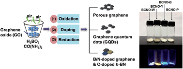
The emission of BCNO phosphors has been easily tuned from the violet to the near red regions by varying the carbon content. Here we report the optimal conversion of graphene oxide (GO) into BCNO hybrid nanostructures by one-step air oxidation with boric acid and urea. White lighting phosphor was obtained in which the doped porous graphene acts as an interconnecting framework generating and transferring electrons under excitation light. Various carbon-related levels in the BN band structures play an essential role in emitting full colour white light. The quantum confinement in the various kinds of GQDs and GO are also beneficial to widen the emission spectrum.
Graphene oxide (GO) is a marvelous candidate suitable for this target, because it can be either reduced to graphene, or further oxidized to defective smaller ones.4 It is covalently decorated with oxygen-containing functional groups, and contains a mixture of sp2- and sp3-hybridized carbon atoms. Manipulation of the size, shape and relative fraction of the sp2-hybridized domains of GO by reduction chemistry provides opportunities for tailoring its optoelectronic properties.4d–f The tunable PL spectra of GO during reduction are thus attributed to the variation of the relative intensity ratios of PL emission from two different types of electronically excited states.4d It has also been reported that graphene quantum dots (GQDs) have both up-conversion and down-conversion PL properties, which widens their emission spectrum.5 Furthermore, the bandgap of GO can also be easily tuned by incorporating non-carbon elements.4b For example, B/N doped graphene, or BCN compounds, are expected to behave as semiconductors with tunable band gap energies, because these materials are thought to be the intermediates between graphene (0 eV) and hexagonal BN (h-BN, ∼6.0 eV).6
Based on the above results on the tunable PL spectra of BCNO and GO, we used GO as the only carbon source to make BCNO phosphors. In the present study, not only GO itself plays the role in emitting light, but what's more important is the hybrid nanostructures which may have unexpected synergy effects, open many possibilities for white-lighting purpose.
We could obtain different lighting phosphors by varying the raw material ratios and the highest heat treatment temperatures in air, which are listed in Table 1. The phosphors emitting yellow, blue, purple and white light are named as BCNO-Y, BCNO-B, BCNO-P and BCNO-W respectively.
| Phosphors | Weight ratio, (GO/boron acid/urea) | Highest temperature in air (°C) | Powder color under solar light | Emission color excited at 365 nm |
|---|---|---|---|---|
| BCNO-Y | 20/30/600 | 800 | Light gray | Yellow green |
| BCNO-B | 10/30/600 | 800 | White | Greenish blue |
| BCNO-P | 20/30/600 | 750 | White | Purperlish blue |
| BCNO-W | 10/30/600 | 750 | White | White |
The PL spectra of the BCNO phosphors were recorded using a spectrofluorophotometer (FL3, France) equipped with a xenon laser source. The EQE of the prepared particles was determined at an excitation wavelength of 365 nm produced by a 150 W Xe lamp using an absolute PL quantum yield measurement system (Quantaurus-QY, Japan) with an A-10095-01 powder sample holder. The PL decay profiles and the time-resolved emission spectra (TRES) were collected with an FL3 spectrophotometer.
We focused on the BCNO-W phosphor to perform compositional characterizations, which are shown in Fig. 1 and S3 and S4.† XPS full spectrum of BCNO-W (Fig. S3†) indicates the atomic contents of B, C, N and O are 30 at%, 18 at%, 21 at% and 32 at% respectively. XRD patterns (Fig. 1a) indicate the existence of B2O3, BN and graphene (or doped graphene). The typical signal of GO at 11.2° is lost after the reaction, transferring to the typical signal of graphene at 17.5°.4 Graphene-facilitated formation of h-BN has been observed in our previous study,6d so the overlapped signals of BN and graphene at 26.2° and 43.4° may indicate h-BN. FT-IR analysis (Fig. 1b) shows a strong and wide B–O (∼1200 cm−1) band in BCNO–W, which covers the vibrations of C–N (1080 cm−1) and B–C (1100 cm−1). The strong carboxyl C–O (∼1400 cm−1) band of GO becomes nearly disappeared in BCNO–W and a new signal assigned to B–N appears at the same position.6 The above analysis means that graphene nanosheets are present in the hybrid particles, which are isolable and surrounded by boron oxide (nitride) phases.
A deep study on the bonding structure of the BCNO-W hybrid was made using XPS C1s, B1s and N1s profiles, as shown in Fig. 1d–f. According to B1s analysis (Fig. 1e), the main configuration is B–O bonding, and the rest corresponds to B–N and B–C bonding.6c–e It strongly indicates a large fraction of boron oxide phase. The N1s signal (Fig. 1f) can be deconvoluted into four peaks, among which the main one is B–N–C bonding.6 The C1s analysis reveals four kinds of carbon,6b with two new peaks emerging as C–B and C–N bonding, compared to C1s signal of GO (Fig. 1c). In addition, the intensity of C–O bonding is much lower than that of GO. This indicates that GO was almost completely reduced to graphene and doped with B and N at the same time.4,6 Since nitrogen has an atomic fraction of 21 at%, the predominant B–N–C structures (more specifically, B/N doped graphene) may have a weight percent up to 50 wt%. We washed the BCNO–W powder with warm deionized water and recovered reddish residue. A much reduced B–O signal is observed in the B1s signal (Fig. S4†), indicating the removal of most boron oxide. The residue consists mainly of large layers of B-N-C type doped graphene, as indicated from N1s analysis.
Microstructural analysis is shown in the typical SEM and TEM images in Fig. 2 and S5 and S6.† Honeycomb-like morphologies at the micrometer scale could also be observed (Fig. 2a and b). It seems that the ultrathin graphene atomic layers are etched into micro-holes and combined by glue-like boron oxide. TEM characterizations (Fig. 2c–h) demonstrate the presence of nanosheets similar to few-layered graphene. Numerous nanosized holes (Fig. 2e and g) and nanosized inclusions (Fig. 2d and f) could be observed. These inclusions were studied in high resolution and are shown in Fig. 2d and h. They have clear lattice structures with lattice parameters of 0.34 nm or 0.21 nm, corresponding to h-BN or the (1100) lattice fringes of sp2-type graphene.8c Since the diameters are down to 10 nm, they are typical GQDs.5
![]() | ||
| Fig. 2 Microstructural analysis of the BCNO–W phosphor. (a and b) Typical SEM images and (c–h) typical TEM images. | ||
Electron energy loss spectroscopy (EELS) and energy dispersive X-ray spectroscopy (EDS) analysis for the BCNO-W phosphor are shown in Fig. 3 and S6† respectively. Four ionization edges at about 188, 284, 400, and 530 eV are clearly apparent, corresponding to the characteristic K-edges of B, C, N, and O, respectively.2 The results in EDS also confirmed that the particles are composed of B, C, N, and O atoms, with an atomic ratio to be 31
:
10
:
30
:
29. The phosphor was covalently bonded to B, N, and O atoms with a soft (sp2 hybridization) carbon framework via π* and σ* bands, indicating the B-C-N-O quaternary compound.
The incorporation of B and N into graphene (B/N doped graphene) has been studied in detail in our previous report,6d which uses a similar process derived from the same raw materials. So during the heat treatment in air, GO is changing in three different and combined ways: oxidation, doping, and reduction, as shown in Fig. 4. GO is oxidized becoming porous both at the micro- and nano- scales. They are even splitting into much smaller ones down to the quantum dots level. The removal of epoxy, carbonyl and carboxyl groups facilitates this etching and cutting process.9 Both the high temperature and the local ammonia reductive atmosphere make contributions to the O-removal, leading to fully reduced GO, namely, graphene.4,8,9 At the same time, boron oxide and urea or ammonia react with GO to make B and N co-doping, leading to a large fraction of B-N-C type doped graphene.6c–e As expected, a variety of graphene-like carbon of different sizes can be formed in the process.
| Phosphors | Peak emission excited at 365 nm (nm) | CIE coordinate excited at 365 nm, (x,y) | Extenal quantum efficiency (EQE) (%) | First band gap (eV) | Second band gap (eV) |
|---|---|---|---|---|---|
| BCNO-Y | 550 | (0.348, 0.408) | 16.7 | 3.3 | 2.1 |
| BCNO-B | 438 | (0.186, 0.219) | 27.1 | 4.3 | 2.3 |
| BCNO-P | 388 | (0.190, 0.236) | 45.9 | 4.9 | 3.7 |
| BCNO-W | 445 | (0.292, 0.342) | 28.2 | 5.9 | 3.4 |
The band gap of B-N-C is tunable between that of graphene and h-BN.4,6 As shown in Fig. 5c, the first absorption edge of the BCNO-W phosphor is the largest, corresponds to a band gap of 5.9 eV, belonging to the h-BN phases. The second absorption edge of BCNO-W suggests a band gap of 3.4 eV, related to the B-N-C type doped graphene nanosheets.4,6 Interestingly, we found that both these two band gaps were tunble (increased) from yellow, blue and purple to white lighting phosphors. It indicates that lowering the annealing temperature or decreasing the GO loading are all beneficial to the doping and nitridation process, thus increasing the band gap of doped graphene and BN to a proper value for excitation.6c–e
Based on the above results, a modified PL white lighting mechanism is proposed and shown in Fig. 6.2f The doped porous graphene acts as interconnecting framework generating and transferring electrons under excitation light. The 365 nm (3.4 eV) absorption is due to the transition from the valance band to the conduction band. This means that the doping and oxidation open the band gap of graphene to 3.4 eV.6c BN is responsible for the light emission and the 210 nm (5.9 eV) absorption is induced by the transition from the valence band to the conduction band in h-BN.2d–f The nitrogen vacancy level is 0.7–1.0 eV lower than that of the conduction band,10 which is supposed to trap electrons forming paramagnetic luminescence centers.2d Carbon components form a series of new levels under the nitrogen vacancy level, including the levels of interstitial carbon, substitutional CB and CN and carbon impurity. These levels are ∼1.7 eV, ∼2.2 eV and ∼3.4 eV lower respectively than the nitrogen vacancy level.10,2 As reported,10b the interstitial carbon with different sized GQDs can generate deep levels (2–4 eV) below the conduction band. So, the transition from the conduction band or nitrogen vacancy level to the various carbon related levels will emit full visible colors, and thus forming white light. GQDs and GO can emit light under irradiation by themselves.5 The size variation of GQDs, as well as the reported tunable PL properties of GO, both related to the quantum confinement effect, have great influences on the variation of their peak emissions.4,5 It can be thought of another beneficial mechanism widening the emission spectrum. It is also regarded that the closed-shell BO− and BO2− anions act as high-efficient luminescence centers,2a in this case, graphene can act as the electron fast transferring agent, increasing the luminescence intensity and the quantum efficiency.4
Footnote |
| † Electronic supplementary information (ESI) available: XPS profiles, SEM and optical properties of the phosphors. See DOI: 10.1039/c4ra02775b |
| This journal is © The Royal Society of Chemistry 2014 |