Nanoparticle attachment on Ag nanorings and nanoantenna for large increases of surface-enhanced Raman scattering†
Zao Yiab,
Jiangshan Luob,
Yong Yic,
Xibin Xuab,
Pinghui Wud,
Xiaodong Jiangb,
Yougen Yi*a and
Yongjian Tang*b
aCollege of Physics and Electronics, Central South University, Changsha 410083, Hunan, China. E-mail: yougenyi@mail.csu.edu.cn; Fax: +86 0816 2480830; Tel: +86 0816 2480827
bResearch Center of Laser Fusion, China Academy of Engineering Physics (CAEP), Mianyang 621900, Sichuan, China. E-mail: myyz1984@mail.csu.edu.cn; Fax: +86 0816 2480830; Tel: +86 0816 2480827
cJoint Laboratory for Extreme Conditions Matter Properties, Southwest University of Science and Technology and Research Center of Laser Fusion, CAEP, Mianyang 621900, Sichuan, China
dState Key Laboratory of Modern Optical Instrumentation, Department of Optical Engineering, Zhejiang University, Hangzhou 310027, Zhejiang, China
First published on 8th May 2014
Abstract
A simple and inexpensive approach based on the heat-treatment of Ag+/PVA/PVP composite film on quartz glass has been developed for fabricating large-area Ag nanorings attached small nanoparticles. The explosive decomposition of AgNO3, PVA and PVP by calcination could explain their formation. A maximum enhancement factor of 1.9 × 10¹⁰ can be obtained with the self-organized Ag nanorings attached small nanoparticles. Moreover, using the three-dimensional finite-difference time-domain (3D-FDTD) simulations, we stipulate that the EF can be obviously improved via some small Ag particle attachment on these nanorings because of the strong coupling between the discrete plasmon states of the small nanoparticles and the term of propagating plasmons of the Ag nanorings. Understanding and realization of the enhancing mechanism of nanostructured surface attachment small nanoparticles could have potential to effectively improve the SERS property of the SERS substrates.
1. Introduction
In 1974, Fleischmann et al. first observed surface-enhanced Raman scattering (SERS).1 After that, based on this important technique for trace molecular analysis, many fundamental research and practical applications have been extensively studied.2–4 Two mechanisms are often put forward in previous papers to explain the SERS characteristics. The first one is the electromagnetic mechanism (EM), and the second one is the chemical mechanism (CM). The EM mechanism is responsible for the major of SERS enhancement that could give up to 1012 enhancement. However, the CM mechanism is considered to be usually in the range of 10–100.5 These “hot spots” on the metal surfaces, which are regions with a high intensity of an EM field in the enhancement mechanism of SERS, play an important role.6,7 “Hot spots” can be obtained at the adjacent site between metallic nanoparticles or at locality outside of a sharp surface protrusion, such as in the gap of aggregated colloids,8 at junctions of fabricated nanostructures,9 as well as on the apexes of metallic tips.10 Thus, preparing substrates with lots of “hot spots” is one of the most important tasks in this field.Metal nanoring structures are particularly attractive because these structures can induce a strong local electric field owing to plasmons forcefully coupled at the interior and exterior surfaces.11,12 Moreover, by changing the size and width of the ring, the nanoring exhibits strongly tunable plasmonic resonance from the visible to near-infrared (NIR) region.13 These properties of nanoring, including optical antennas,14 plasmonic waveguide,15 optical confinement,16 data storage17 and SERS,18–20 have been used in applications. To fabricate metal nanorings, a variety of methods have been reported including lithography,21,22 molecular-beam epitaxy23 and template techniques.24,25 Generally speaking, template methods seem to be important for the preparation of such interesting nanoparticles, no matter what various post treatment is used. Moreover, these templates include polystyrene (PS) nanospheres,26 mesoporous membrane,27 DNA condensates28 and porous anodic aluminum oxide.29 However, because of technical or economic perspectives, most of these techniques either involve complicated procedures or sophisticated instruments, which could limit their use for the large-scale production of rings. Thus, for sensing applications, a functional, reproducible, and low cost nanoring structure SERS active substrate is required to enable Raman measurements of various analytes.
Here, in this paper, we provide a convenient and low cost way for the large-area self-organized synthesis of Ag nanorings attached small nanoparticles through heat treatment of Ag+/PVA/PVP composite film on quartz glass. Because templates and sophisticated apparatus are not necessary, the synthesis provided here can be an important addition to existing methods for the fabrication of rings. In addition, the as-prepared special structural features of nanoparticle-attached Ag nanorings have been applied in SERS properties with rhodamine 6G (R6G) and 4-aminothiophenol (4-ATP) as the probe molecules. Using the three-dimensional finite-difference time-domain (3D-FDTD) simulation, the theoretical examination of the local EM properties lets us evaluate the contributions of the nanorings and nanoparticle-attached Ag nanorings to the experimentally obtained SERS intensities. Using simulations, we stipulate that the weak enhancement can be remarkably improved through nanoparticle-attached Ag nanorings and by utilizing transversely polarized light. In addition, we provide strong lateral coupling induced at the adjacent site between the small Ag nanoparticles and nanoring.
2. Experimental details
In the experiment, at first, we prepared an aqueous mixture containing 50 ml of AgNO3, 50 ml of poly(vinylpyrrolidone) (PVP) and 50 ml of poly(vinylalcohol) (PVA). The mole ratio of PVA, PVP and AgNO3 was tuned from 4![[thin space (1/6-em)]](https://www.rsc.org/images/entities/char_2009.gif) :1:3, pass 4:1:4 and 4:1:5, to 4:1:6. Then, we spin-coated the mixture at 3000 rpm for 3 min on a quartz glass wafer, and the number of spin coats is one, two and three. Subsequently, we dried these films in a vacuum overnight and then reduced the prepared Ag+/PVA/PVP film by aqueous H2O2 or calcined the Ag+/PVA/PVP film without reduction. In the former experiment, we immersed the prepared Ag+/PVA/PVP film into 10 mM aqueous H2O2 for 10 min, then the film was rinsed with deionized water, and then dried in a vacuum overnight. Lastly, we calcined these spin-coated films at a rate of 2 °C min−1 from room temperature to 700 °C. In this process, we kept the samples at 700 °C for 4 hours under an Ar gas atmosphere, and finally we allowed these films to cool.
:1:3, pass 4:1:4 and 4:1:5, to 4:1:6. Then, we spin-coated the mixture at 3000 rpm for 3 min on a quartz glass wafer, and the number of spin coats is one, two and three. Subsequently, we dried these films in a vacuum overnight and then reduced the prepared Ag+/PVA/PVP film by aqueous H2O2 or calcined the Ag+/PVA/PVP film without reduction. In the former experiment, we immersed the prepared Ag+/PVA/PVP film into 10 mM aqueous H2O2 for 10 min, then the film was rinsed with deionized water, and then dried in a vacuum overnight. Lastly, we calcined these spin-coated films at a rate of 2 °C min−1 from room temperature to 700 °C. In this process, we kept the samples at 700 °C for 4 hours under an Ar gas atmosphere, and finally we allowed these films to cool.
In the SERS spectra measurements, first of all, by using an accurate pipette, we dropped a 10 μl droplet of a 1.0 × 10⁻⁶ mol l−1 ethanol solution of 4-aminothiophenol (4-ATP) or 1.0 × 10⁻⁶ mol l−1 aqueous solution of rhodamine 6G (R6G). Secondly, the samples were dried in air at ambient temperature in order to gain a uniform molecule membrane over an area of about 10 mm2. In this experiment, we prepared three samples with the same SERS-active substrates. In addition, each sample was used to select ten different points in order to detect the 4-ATP or R6G probes, which confirm the reproducibility and stability of these samples. We used a Renishaw 2000 model confocal microscopy Raman spectrometer, which includes a CCD detector and a holographic notch filter to measure the SERS spectra. A Leica DMLM system was adopted in the microscope attachment. The laser beam was focused onto a spot about 1 μm in diameter by using a 100× objective. The SERS was excited using radiation of 514.5 nm from an air-cooled argon ion laser, which was about 7.2 mW at the position of samples. The recorded time of the Raman spectra is 20 s.
3. Simulation methods
We used a commercial FDTD calculation for the 3D-FDTD simulations.30 The boundary conditions of the simulation domain are perfectly matched layer absorbing boundaries. The calculation region is 0.8 × 0.8 × 0.2 μm3, and the cell size is 1 × 1 × 1 nm3. We installed propagation directions of plane waves parallel with the x-axis. In order to closely match the experimental conditions, the model of the Ag nanostructures was introduced. Fig. 1 shows the schematic geometries of the structures studied. The scheme of the Ag nanoring with an outer radius r1 (r1 = 250 nm), inner radius r2 (r2 = 150 nm) and thickness h (h = 100 nm) is shown in Fig. 1a. The scheme of the Ag nanosphere with a radius r (r = 250 nm) is shown in Fig. 1b. Fig. 1c and d shows these models of the Ag nanoring attached to one small Ag nanoparticle at different sites: (c) interior surface and (d) exterior surface. We set the simulation time to be 300 fs, and the input pulse width is 14.70 fs in order to ensure the fields decay completely. In our simulation, the dielectric function of the Ag nanostructure was described by the Lorentz–Drude model.31 The refractive index of the surrounding medium was set to be 1.0 for air and the dispersion of the quartz glass substrate was considered. The dielectric constants of the glass have been taken from Palik.32 The near field intensity enhancement images are set up by dividing the electric field strength (E2 = Ex2 + Ey2 + Ez2) around the Ag nanostructure. In the simulation, first of all, we calculated the local electric field, and then evaluated the field intensity for each mesh through integration. Lastly, we compared the computation with the EF values, which were obtained from the measured Raman spectra.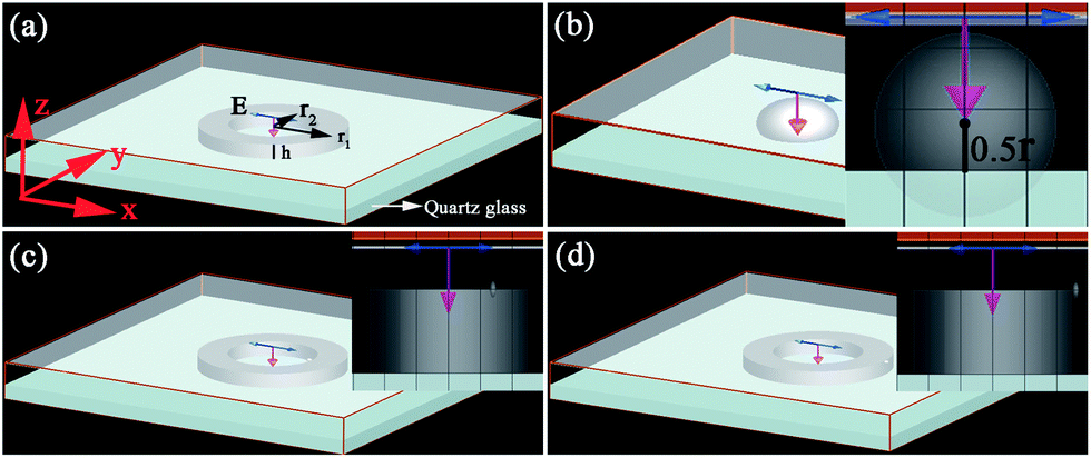 | ||
| Fig. 1 (a) The model of the Ag nanoring; (b) the model of the Ag nanosphere; (c) the model of Ag nanoring attached to one small Ag nanoparticle on the interior surface; (d) the model of Ag nanoring attached to one small Ag nanoparticle on the exterior surface. | ||
4. Results and discussion
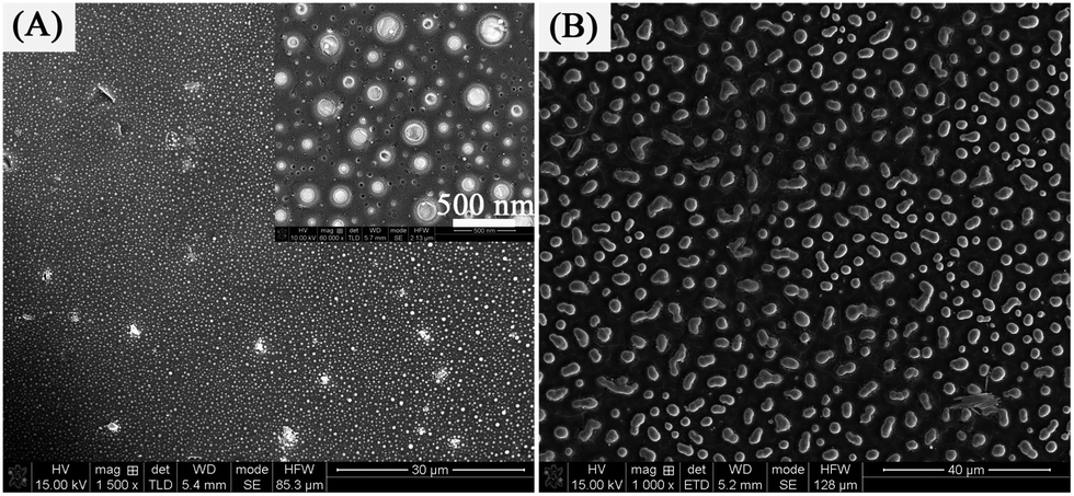
On the basis of the heat treatment of the Ag+/PVA/PVP composite film on quartz glass wafer, we can obtain large-area self-organized Ag nanorings attached small nanoparticles. During the high temperature, the organic components are removed, AgNO3 is decomposed into Ag0, and nitrogen, oxygen, and nitrogen oxides are released. The Ag0 species produced were unstable and could aggregate to form Ag clusters. The SiO2 layer of quartz glass wafer forcefully interacts with Ag0 and will decrease the activity of Ag0. The activity of Ag0 can be decreased with aggregation and the particle size is increased. Through the strong bonding interaction between the outmost orbital of the Ag nanoparticle surface atoms and the contacting oxygen atoms of the quartz glass wafer, these metal nanoparticles will be stabilized,33,34 and the morphologies can be controlled by the experimental conditions. Fig. 2 shows the images of the Ag nanorings attached small nanoparticles. The Ag+/PVA/PVP film is in two layers. The mole ratio of PVA, PVP and AgNO3 is 4:1:4. Self-organized Ag nanorings attached small nanoparticles were formed when the as-prepared Ag+/PVA/PVP film was subjected to calcination without reduction. The low magnification SEM image (in Fig. 2A) obviously shows homogenously distributed self-organized Ag nanorings attached small nanoparticles covering large areas. In Fig. 2B, the high magnification SEM image shows the products are all ring-shaped with an average outer diameter (∼500 nm) and inner diameter (∼300 nm). Very interestingly, lots of small nanoparticles with an average diameter of 20 nm are observed around the Ag ring, which are expected to provide lots of “hot spots” for chemical catalysis. The reason is that the distribution of the small Ag seeds is not homogeneous on the substrate surface at the beginning of the heat treatment. These particles that are close enough would collide and fuse with each other via thermal treatment, forming a larger nanoparticle and leaving a blank area surrounding it. On the contrary, these nanoparticles would stay intact when they are located far enough. Fig. 2C and D show the tilted-view (ca. 15°) SEM images of the self-organized Ag nanorings arrays. Using atomic force microscopy (tapping mode), the structure of the Ag nanorings was further confirmed (as shown in Fig. 3). Fig. 3A shows that these products are all nanoring shaped, which is consistent with the SEM study (as shown the Fig. 2). The deep color in the nanoring is the hole of the nanoring. Fig. 3B gives the 3D image of the Ag nanorings; moreover, the image confirms that the Ag nanorings have an average thickness of 100–150 nm. The detailed morphology analyses have been reported in our previous paper.35
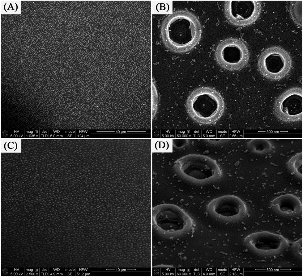 | ||
| Fig. 2 [(A) and (B)] Typical top-view SEM images of the Ag nanorings (sample 1) on a quartz glass wafer,35 [(C) and (D)] tilted-view (ca. 15°) SEM images of the Ag nanorings on a quartz glass wafer. | ||
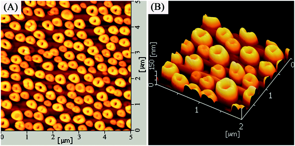 | ||
| Fig. 3 AFM and 3D image of the Ag nanorings (sample 1) on a quartz glass wafer. | ||
PVA and PVP are well known organic polymers, which are mostly used as a water-soluble organic binder. In the past several years, as a template and a capping agent for nanoparticles synthesis, PVA and PVP have been used widely.36,37 In our study, the mole ratio between PVA, PVP and AgNO3 can control the shape of the Ag nanoparticles. As shown the Fig. 4, there are two types of morphology for the Ag nanoparticles, one is a nanoring and the other is hemispherical or spherical, are obvious on the surface of quartz glass wafer. Fig. 4A, corresponding to the mole ratio of 4:1:3 (sample 2) shows lots of monodisperse Ag nanorings covering the quartz glass wafer surface. When compared to the nanorings prepared with the mole ratio of 4:1:4, as shown the Fig. 4B, the average size (the Fig. 4A) is much smaller with an outer diameter of 300 nm and inner diameter of 120 nm. However, as shown the Fig. 4C, lots of Ag nanoparticles with an inhomogeneous size appear on the quartz glass wafer surface when the AgNO3 concentration rises to 4:1:5 (sample 3). Note that the shape of nanoparticles is hemispherical and spherical; however, in Fig. 4D, no nanorings can be found but particles with bigger size, corresponding to the mole ratio of 4:1:6 (sample 4) can be observed. The diameter of the particles and ratio of big size particles increase dramatically when the AgNO3 concentration increases. The SEM research shows that the Ag products experience an evolution of size and morphology that the size changes from small to big and the morphology changes from nanoring to nanosphere. In other words, the mole ratio of PVA, PVP and AgNO3 plays a significant role in our study. The reason is that it determines the distance of the Ag particles and clusters, by which the particles and clusters will aggregate via different modes. If the AgNO3 concentration is very high, due to the close distance, these Ag nanoparticles and nanoclusters could aggregate to each other to form a hemispherical or spherical morphology easily. However, if the AgNO3 concentration is very low, due to the relatively long distance, these Ag nanoparticles and nanoclusters could aggregate to form a low dome morphology. As the annealing process goes on, as shown the Fig. 4C and D, these hemispherical and spherical-shaped Ag aggregates will grow to metallic Ag without any change in their morphology. However, these dome-shaped Ag aggregates contain many unreleased organic composites and HNO3. As shown the Fig. 4A and B, the release of gaseous CO2, H2O and NO2 will break through the top of the dome when the temperature rises high enough; thus, these dome-shaped Ag aggregates form ring-like shapes.
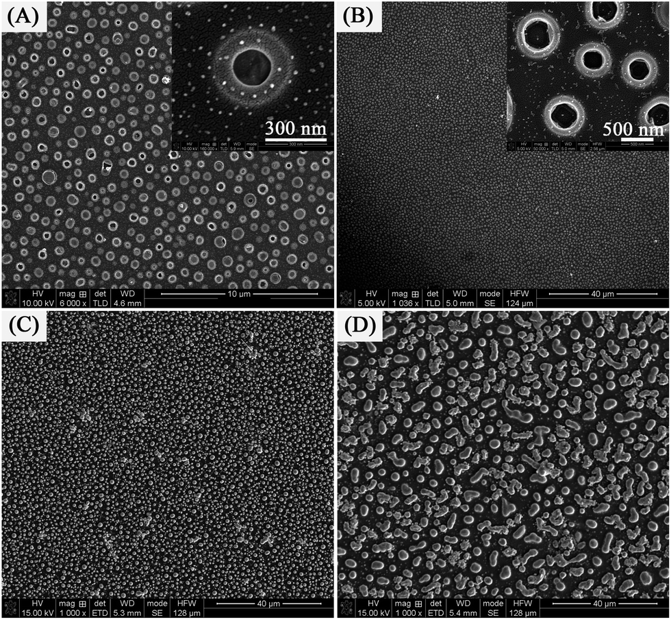 | ||
| Fig. 4 SEM images of the Ag nanoparticles obtained from different mole ratios of PVA, PVP and AgNO3. A, B, C and D are corresponding to the mole ratio of 4:1:3 (sample 2), 4:1:4 (sample 1), 4:1:5 (sample 3) and 4:1:6 (sample 4), respectively. The inset images are the magnified SEM images of the corresponding samples. | ||
The thickness of the prepared spin-coated films can also influence the morphology of the nanoparticles. As mentioned in our experiment, these films have different thickness as a result of the different number spin coats. Fig. 5 represents the SEM images of the Ag+/PVA/PVP composite film with different thickness. The SEM images show that the formation process of the ring nanostructure can be controlled by the thickness of film. When the spin coat is one, as expected the shape of the nanoparticles is a nanoring, as shown the Fig. 5A. However, when the spin coat is three, lots of bigger size particles are prepared and no Ag nanorings can be found, as shown the Fig. 5B. It can be seen that these Ag nanoparticles and nanoclusters could aggregate to each other to form a hemispherical or spherical morphology easily due to the close distance. On the basis of the above experimental results, the optimal spin coat for the formation of Ag nanorings is two coats.
 | ||
| Fig. 5 SEM of the Ag nanoparticles prepared by different spin coats: (A) one coat (sample 5); (B) three coats (sample 6). The mole ratio of PVA, PVP and AgNO3 is 4:1:4. The inset images are the magnified SEM images of the corresponding samples. | ||
It is useful to speculate on the mechanism of Ag nanoring formation in this experiment. Note that Ag+/PVA/PVP were composed by PVA and PVP that serve as a binder. The hydroxyl groups of PVA and PVP act as ligands to the Ag+. These hydroxyl groups are necessary for the homogeneous dispersion of Ag+. The prepared spin-coated films are composed of PVA, PVP and small Ag nanoparticles. At the beginning, the aqueous AgNO3, PVA and PVP are a colorless precursor solution. After stirring for one hour at room temperature, they become deep yellow and then later turn darker, indicating that small Ag nanoparticles appear in the aqueous mixture.38 In order to transform more Ag+ into Ag0, we immersed the prepared Ag+/PVA/PVP film (two layers) on quartz glass wafer into aqueous H2O2. Then, the film was rinsed with deionized water, and dried in vacuum overnight. Fig. 6 represents the SEM image of the as-treated film by aqueous H2O2. We can see lots of small Ag nanostructures that are reduced by the PVA, and PVP distributed on the substrate surface. These small nanoparticles and nanoclusters are embedded in the PVA/PVP composite,38 and the large particles with diameters of 20 nm are reduced by H2O2. Fig. 7 is the 3D image of the nanoparticles on the quartz glass wafer with different experimental conditions. In Fig. 7, Fig. 7A shows the heat treatment of the Ag+/PVA/PVP composite film after reduction by H2O2, Fig. 7B shows the heat treatment of the Ag+/PVA composite film without reduction and Fig. 7C shows the heat treatment of the Ag+/PVA/PVP composite film without reduction, and all these films have two layers. When the Ag+/PVA/PVP composite film was reduced by H2O2, lots of large particles (∼20 nm) appeared, as shown the Fig. 6. From Fig. 7A, these large silver aggregates grow to hemispherical and spherical silver nanoparticles without any change in the morphology. The 3D image of the Ag nanoparticles confirms the hemispherical and spherical Ag nanoparticles with an average thickness of 150–200 nm. The SEM image of the Ag nanoparticles prepared after reduction by H2O2 is shown in Fig. S1,† and the average diameter is about 500 nm. As we know, the decomposition peak of PVA is at approximately 300 °C in the derivative TGA curve.39 Moreover, the decomposition peak of PVP is at approximately 380 °C in the derivative TGA curve.40 In our experiment, through the different decomposition temperature of the PVA and PVP, we could obtain the Ag nanorings on the quartz glass wafer. Fig. 8 shows the TGA thermogram of the Ag+/PVA/PVP composite film. The mole ratio of PVA, PVP and AgNO3 is 4:1:4. The thermogram was collected in an Ar gas atmosphere (200 ml min−1) from 50 °C to 1000 °C at a heating rate of 10 °C min−1. PVA chains are going to change to a crosslinked polymer after high temperature treatment (250 °C) when the annealing process begins. When the temperature rises to 300 °C, the PVA will be decomposed and removed. These Ag+/PVA particles, which contain NO3− and PVA molecules will decompose, and then release gaseous N2, O2, CO2, H2O, and nitrogen oxides via thermal treatment. During the process, because of the gas release, the large Ag+/PVA particles probably expand via thermal treatment to collapse, and later to metal nanorings. However, as shown the Fig. 7B, when the heat treatment film is the Ag+/PVA composite film, the production are not all nanorings, and these nanorings do not exhibit distinctness. AFM images and the section analysis obtained by AFM are shown in Fig. S2,† and the results obtained are similar to those previously reported.34 When the temperature rises highly enough to 380 °C, the PVP molecules in the nanoparticles undergo decomposition. Then, the release of CO2, H2O and NO2 gas will break through the top or side of these spherical Ag nanoparticles again; thus, the nanoparticles come into being with ring shapes, as depicted from Fig. 7C. From these contradistinctive experiments, we know that the gas release from the PVP is very important for the formation of nanorings.
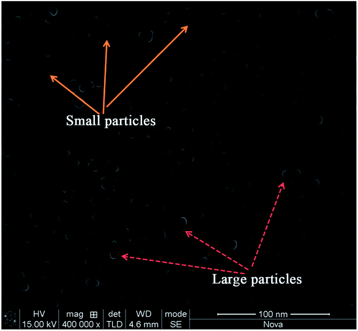 | ||
| Fig. 6 SEM image of the Ag/PVA/PVP film (two layers) after reduction by H2O2, where the solid and dotted arrows point to the small particles and large particles, respectively. | ||
 | ||
| Fig. 7 3D images of the nanoparticles on a quartz glass wafer with different experimental conditions: (A) heat treatment of Ag+/PVA/PVP composite film with reduction35 (sample 7); (B) heat treatment of Ag+/PVA composite film without reduction (sample 8); (C) heat treatment of Ag+/PVA/PVP composite film without reduction35 (sample 1). These films are two layers. | ||
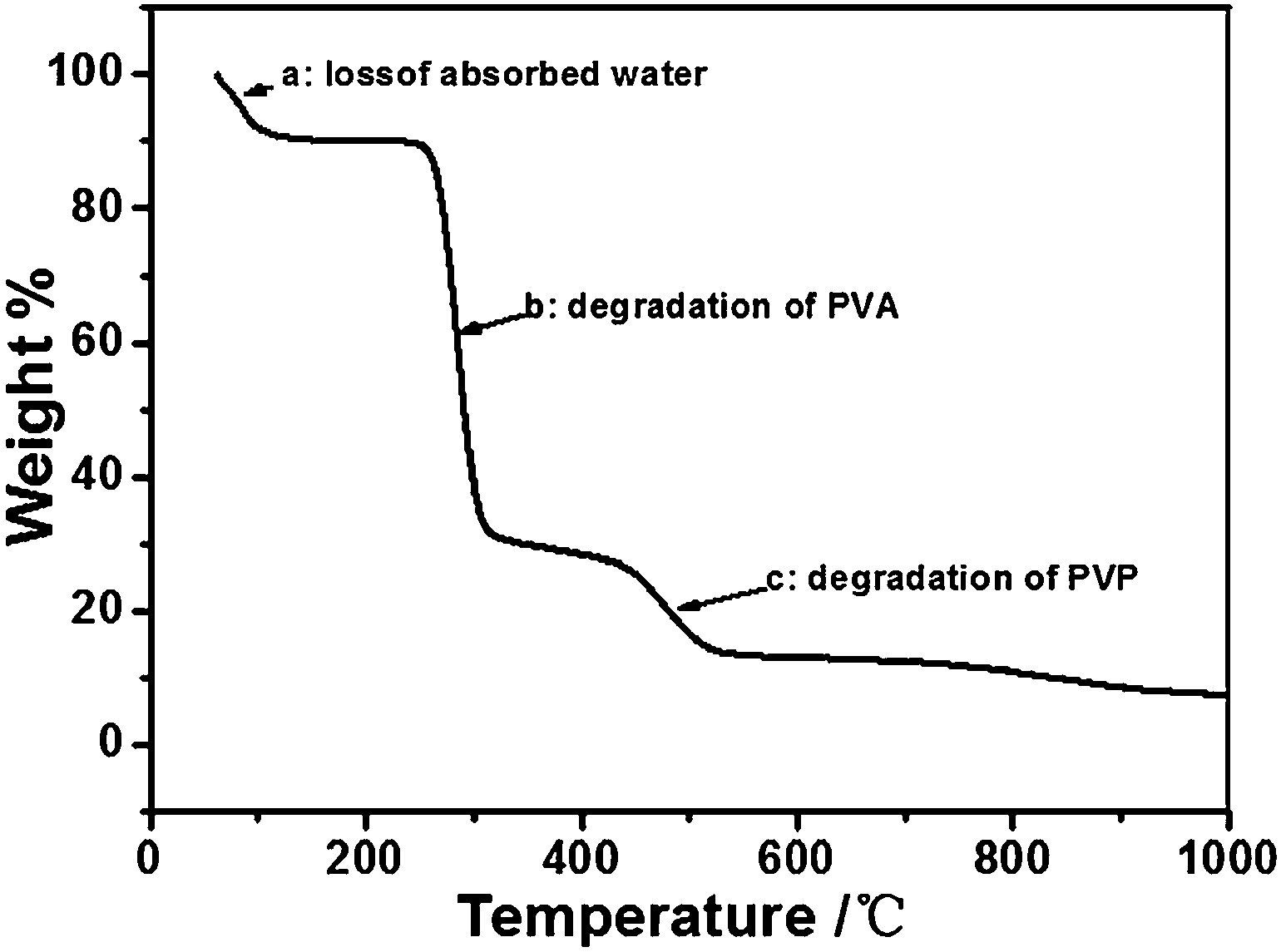 | ||
| Fig. 8 TGA analysis of the Ag+/PVA/PVP composite film. The mole ratio of PVA, PVP and AgNO3 is 4:1:4. | ||
Since Ag nanorings display different electric field characteristic when compared to Ag spherical nanoparticles, this may lead to a large SERS enhancement. To investigate the SERS sensitivity of the Ag nanoparticles substrates, the SERS spectra of 4-ATP were measured under the same experimental conditions (laser power = 50 μW, microscope objective = 50×, acquisition time = 20 s) using Raman spectroscopy. As shown the Fig. 9, the black, red and blue lines correspond to sample 1, sample 7 and sample 8, respectively. Two kinds of bands were observed on the SERS spectra of 4-ATP on the Ag nanoparticles film. One kind is located at 1073 and 1185 cm−1, which are assigned to the a1 vibration modes, and the other kind is located at 1143, 1388, 1436, and 1577 cm−1, which are assigned to the b2 vibration modes.41 The intensity increase of the b2 and a1 modes is associated mainly with the CM and EM effect, respectively.42 Therefore, the SERS enhancement of our samples comes from both CM and EM effects. Obviously, the EF is improved when the 4-ATP molecules are absorbed on the Ag nanoring structure (sample 1). We strongly believe that the strong SERS effect on the Ag nanoring structure is caused by two effects. The first one is the EM mechanism due to the strong coupling of the LSP of the Ag nanorings. The second one is the CM effect that induced the charge transfer (CT) behavior between the Ag nanorings and 4-ATP molecules. Because of the inner region of the Ag nanorings, the inner region of the nanorings can offer suitable active sites for the detection of molecular binding. This structure can be considered as the Ag/4-ATP/Ag sandwich structure, the charge transfer model of the “donor–bridge–acceptor” system may be possible to the present structure.
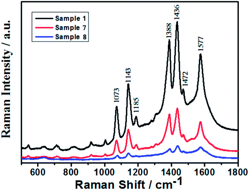 | ||
| Fig. 9 SERS spectra of 4-ATP (1 × 10⁻⁶ M) on the Ag nanoparticles film prepared with different experimental conditions. The black, red and blue lines correspond to sample 1, sample 7 and sample 8, respectively. | ||
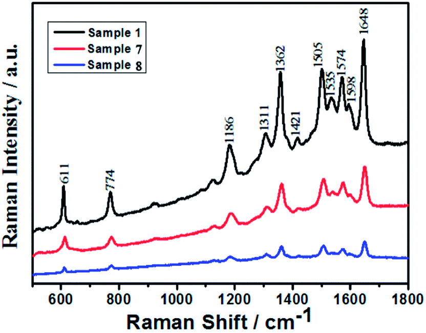
To investigate the enhancement factor (EF) of these structures quantitatively (sample 1, sample 7 and sample 8), here we take R6G as the test molecule. Fig. 10 presents the SERS spectrum of R6G with different samples (sample 1, sample 7 and sample 8), the concentration is 1 × 10⁻⁶ M. We have assigned the spectral traits of R6G in detail previously; thus, we will not repeat them here again.43 As shown, the R6G molecules on the hemispherical and spherical Ag nanoparticles film (sample 8) displayed very light SERS signal. However, the R6G molecules on the Ag spherical nanoparticles and nanorings film (sample 7) displayed a medium SERS signal. Compared to the response of sample 7, sample 1 (Ag nanorings film) displayed a much stronger SERS response. These different SERS enhancements can be revealed by the comparison of these spectra, especially the quantitative intensity comparison from the band at 1648 cm−1. To determine the enhancement effect (EF) of R6G on the nanoparticles quantitatively,44,45 the EF values of R6G in the nanoparticles are calculated with the following expression (the detailed calculation can be found in the ESI†):

 | ||
| Fig. 10 SERS spectra of R6G (1 × 10⁻⁶ M) on the Ag nanoparticles film prepared with different experimental conditions. The black, red and blue lines correspond to sample 1, sample 7 and sample 8, respectively. | ||
Then, the EF for the sample 1, sample 7 and sample 8 were roughly estimated by comparing the peak intensity at 1648 cm−1 to 1.9 × 10¹⁰, 2.9 × 10⁹ and 9.8 × 10⁸, respectively. The SERS spectrum of the Ag nanorings film substrate reveals SERS signals about 16 times larger than the Ag spherical nanoparticles film substrate. The absorption spectra of the Ag nanoparticles on a quartz glass wafer with different experimental conditions are shown in Fig. S3.† The SERS enhancement probably related to the following factors. First of all, the larger surface area of the Ag ring nanostructures can induce the SERS enhancement (as shown the Fig. 4). Lots of “hot spots” created at the inner of the nanorings could also be contributors to this increased response. Thus, the strong SERS enhancement appears to be in the middle of the nanorings, even though these probe molecules appear on the nanorings' interior or exterior surface. Secondly, the strong intense electromagnetic field can be produced in the nanoring structures. The strong field enhancement suggests that the interior surface of the Ag nanorings can afford suitably active sites for detection of molecular binding, even for biosensor applications. These biomolecules in the surrounding media can be generally accessible to the region inside of the nanorings, unlike in conventional nanoshells. The result can make nanorings advantageous for use in SERS applications.12 In our case, because of the coupling between the discrete plasmon states of the small nanoparticles and the term of propagating plasmons states of the nanorings, the SERS enhancement could be even stronger when small nanoparticles are attached on the Ag nanorings. The junction of the small nanoparticles and nanorings can serve as the hot sites.
The 3D-FDTD method was applied to compute the electromagnetic field distribution that surrounds the laser-illuminated Ag nanorings by numerically solving Maxwell's equations in order to further investigate the physical mechanism of SERS enhancements of the Ag nanorings (as shown in Fig. 11). The SERS effect of the Ag nanorings could be further improved by attaching small Ag nanoparticle due to lots of “hot spots” formed at the interface between nanoparticles, as shown the SEM image in Fig. 2B. Fig. 11A–C shows the E-field amplitude patterns from the theoretical calculations at an excitation wavelength of 514.5 nm for Ag nanorings attached one small Ag nanoparticle on the exterior surface. The diameter of the small Ag nanoparticle is 20 nm. When the polarization direction changes from 0° to 90°, the maximal electric field strength (|E|/|E0|)2 (E is the local fields, E0 is the input fields.) is found to be about 5.2 × 10³, 510 and 62 for the three models (the color bars of Fig. 11A–C. The units are (V m−1)2), respectively. For SERS, it is widely believed that |(|E|/|E0|)|4 is the factor for the increase in Raman intensity.46 The maximum SERS enhancements on the three models correspond to 2.7 × 10⁷, 2.6 × 10⁵ and 3.8 × 10³, respectively. When compared with the isolated Ag nanoring, the field intensity of the Ag nanoring attached to one small Ag nanoparticle is much stronger (as shown the Fig. 11A), the reason is that the Ag nanoring attached nanoparticle mode can make electromagnetic energy successively transfer at the adjacent site, so as to give an extremely large field concentration. Briefly, the discrete plasmon modes of the small Ag nanoparticles couple with the term of propagating plasmons modes of the Ag nanorings. The virtual states can be created by coupling between the discrete and continuous modes. These surface charges on the adjacent regions of the small nanoparticle and nanoring can provide a stronger electric field enhancement. Lots of localized discrete plasmon modes can be created by the hybridization between the nanoring and the small Ag nanoparticle.47 In addition, some of modes can be shifted to the visible or near infrared region. A strong coupling could appear when the wavelength of a plasmon mode is in the vicinity of the Raman excitation wavelength. As shown in Fig. 11A–C, when the polarization direction becomes small, the EF could be increased 3–4 orders of magnitude. When its polarization direction is changed, the localized surface plasmon (LSP) coupling will be newly distributed between the two nanoparticles. The EF enhancement was suppressed by the LSP coupling “delocalization” and “distribution”, the reason is that a parallel orientation of the LSP coupling, which coupled with polarization, is essential for getting extremely light intensity. Because the tensor mode polarization is the key for nonlinear optical phenomena, this will be more preferable for EF enhancement.48 Therefore, the polarization of incidental light could clearly control the nanoparticles surface plasmonic field distribution. Here, we have studied the local electric field distribution of the Ag nanoring attached to one small Ag nanoparticle at the interior surface, as shown the Fig. 11D–F. When compared with the Ag nanoring attached to one small Ag nanoparticle on the exterior surface, as shown Fig. 11A–C, the maximal electric field strength (|E|/|E0|)2 is increased with the same polarization direction and diameter of small Ag nanoparticle. For example, as shown the Fig. 11D, the maximal electric field strength (|E|/|E0|)2 at the junction of particles is about 8.0 × 10³ that is larger than 5.2 × 10³ (Fig. 11A). The reason is that the local electric field distribution of the nanoring is different at the interior and exterior surfaces.
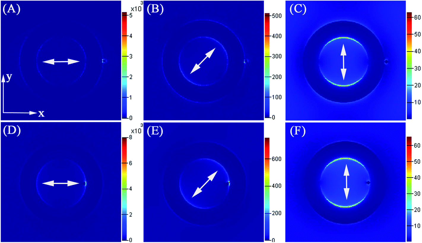 | ||
| Fig. 11 E-field amplitude patterns from the theoretical calculations at the excitation wavelength of 514.5 nm for: (A–C) the Ag nanoring attached to one small Ag nanoparticle on the exterior surface; (D–F) the Ag nanoring attached to one small Ag nanoparticle on the interior surface. The diameter of the small Ag nanoparticle is 20 nm. The arrows represent the different polarization directions: (A and C) 0°, (B and E) 45°, and (C and F) 90°. | ||
As we know the local EM enhancement would increase when the particle size is increased. However, because of inelastic scattering, these particles would absorb less light and scatter more when the particle size increased.49 So the overall SERS intensity would decrease. Moreover, the total surface area of adsorption would decrease when the amount of nanoparticles was fixed and the size of nanoparticles was increased. This reason would offset the increased EM field for larger particles.50 Therefore, it is very significant to confirm the optimal size of the attached Ag nanoparticle to solve the balance problem between scattering limited surface area and EM field increase, so as to realize the strongest SERS intensity. Here, for the model four (as shown the Fig. 1d), we have changed the diameter of the attached small Ag nanoparticle from 15 nm to 30 nm only, and the diameter of nanoring was kept the same. The input light is polarized along the x-axis. As shown the Fig. 11A and 12, the EF of the five models increase in a series: 10 nm < 15 nm < 30 nm < 25 nm < 20 nm, on the basis of the 3D-FDTD calculation results of the maximum field enhancement ((|E|/|E0|)2). According to the connection dynamic depolarization and radiation dampening corresponding to the surface scattering, Meier et al. have predicted the optimal diameter of Ag nanoparticles is 25 nm for SERS.51 However, in our study, the small Ag nanoparticle attached to the big nanoring could have increased the resultant EM field assuming equal excitation. In addition, the shorter wavelength absorption of the smaller nanoparticles could cause a decrease in the excitation of smaller nanoparticles. Therefore, the small Ag nanoparticle (D = 20 nm) is likely to be more appropriate for a higher field enhancement. So, the small attached Ag nanoparticle (D = 20 nm) can provide the strongest SERS enhancement factor.
 | ||
| Fig. 12 E-field amplitude patterns from the theoretical calculations at the excitation wavelength of 514.5 nm for the Ag nanoring attached to one different diameter small Ag nanoparticle on the exterior surface: (A) 10 nm, (B) 15 nm, (C) 25 nm, (D) 30 nm. | ||
5. Conclusions
In summary, large-area self-organized Ag nanorings attached to small nanoparticles have been synthesized on a quartz glass substrate by a simple and convenient heat treatment approach. The typical Ag nanorings attached to small nanoparticles were synthesized as following: the molar ratio of PVA, PVP and AgNO3 is 4:1:4, the Ag+/PVA/PVP composite film was not reduced, and the number of spin coats is two. Using 3D-FDTD simulations, we have shown that the weak enhancement can be remarkably improved through nanoparticle-attached Ag nanorings and the utilization of transversely polarized light. The creation of Ag nanorings attached to one small Ag nanoparticle junctions led to a relatively uniform enhancement of 2.7 × 10⁷, over 4 orders of magnitude stronger than that of the Ag nanoring alone. It can be found that the EF of three kinds of Ag nanoring attached to one small Ag nanoparticle with different polarization directions increased in the series: 90° < 45° < 0°. When compared with the Ag nanoring attached to one small Ag nanoparticle on the exterior surface, the maximal electric field strength (|E|/|E0|)2 of the Ag nanoring attached to one small Ag nanoparticle on the interior surface is increased with the same polarization direction. The small attached Ag nanoparticle (D = 20 nm) with the Ag nanoring can provide the strongest SERS enhancement factor. We hope these methods can provide helpful guidelines for the development of SERS properties.
Acknowledgements
The work is supported by the National Natural Science Foundation of China (no. 10804101; 60908023; 11375159), Science and Technology Development Foundation of Chinese Academy of Engineering Physics (no. 2010B0401055), Open Foundation of Joint Laboratory for Extreme Conditions Matter Properties, Southwest University of Science and Technology and Research Center of Laser Fusion, CAEP (no. 12zxjk07), Scholarship Award for Excellent Doctoral Student granted by Ministry of Education (1343-76140000014), Hunan Provincial Innovation Foundation for Postgraduate (no. CX2012B114), and the Open-End Fund for the Valuable and Precision Instruments of Central South University (CSUZC2012032).References
- M. Fleischmann, P. J. Hendra and A. J. McQuillan, Chem. Phys. Lett., 1974, 26, 163–166 CrossRef CAS.
- S. Nie and S. R. Emory, Science, 1997, 275, 1102–1104 CrossRef CAS PubMed.
- C. Yang, Y. T. Xie, M. M. F. Yuen, X. M. Xiong and C. P. Wong, Phys. Chem. Chem. Phys., 2010, 12, 14459–14461 RSC.
- J. Ando, T. Yano, K. Fujita and S. Kawata, Phys. Chem. Chem. Phys., 2013, 15, 13713–13722 RSC.
- K. Yasutaka, T. Yuhei, I. Tamitake and O. Yukihiro, Phys. Chem. Chem. Phys., 2010, 12, 7457–7460 RSC.
- S. L. Kleinman, R. R. Frontiera, A. I. Henry, J. A. Dieringer and R. P. Van-Duyne, Phys. Chem. Chem. Phys., 2013, 15, 21–36 RSC.
- L. M. Tong, H. Wei, S. P. Zhang, Z. P. Li and H. X. Xu, Phys. Chem. Chem. Phys., 2013, 15, 4100–4109 RSC.
- S. L. Kleinman, E. Ringe, N. Valley, K. L. Wustholz, E. Phillips, K. A. Scheidt, G. C. Schatz and R. P. Van-Duyne, J. Am. Chem. Soc., 2011, 133, 4115–4122 CrossRef CAS PubMed.
- X. M. Feng, F. X. Ruan, R. J. Hong, J. S. Ye, J. Q. Hu, G. Q. Hu and Z. L. Yang, Langmuir, 2011, 27, 2204–2210 CrossRef CAS PubMed.
- P. Brodard, M. Bechelany, L. Philippea and J. Michler, J. Raman Spectrosc., 2012, 43, 745–749 CrossRef CAS.
- J. Aizpurua, P. Hanarp, D. Sutherland, M. Käll, W. B. Garnett and F. J. GarcíadeAbajo, Phys. Rev. Lett., 2003, 90, 057401–057404 CrossRef CAS.
- M. L. Elin, A. Joan, K. Mikael and S. S. Duncan, Nano Lett., 2007, 7, 1256–1263 CrossRef PubMed.
- A. W. Clark and J. M. Cooper, Small, 2011, 7, 119–125 CrossRef CAS PubMed.
- H. M. Gong, L. Zhou, X. R. Su, S. Xiao, S. D. Liu and Q. Q. Wang, Adv. Funct. Mater., 2009, 19, 298–303 CrossRef CAS.
- K. Y. Jung, F. L. Teixeira and R. M. Reano, J. Lightwave Technol., 2007, 25, 2757–2765 CrossRef CAS.
- Y. Babayan, J. M. McMahon, S. Li, S. K. Gray, G. C. Schatz and T. W. Odom, ACS Nano, 2009, 3, 615–620 CrossRef CAS PubMed.
- K. P. Chiu, K. F. Lai and D. P. Tsai, Opt. Express, 2008, 16, 13885–13892 CrossRef CAS.
- M. G. Banaee and K. B. Crozier, Opt. Lett., 2010, 35, 760–762 CrossRef CAS PubMed.
- Y. M. Hou, J. Xu, P. W. Wang and D. P. Yu, Appl. Phys. Lett., 2010, 96, 203107–203109 CrossRef PubMed.
- J. Ye, S. Masahiko, L. Kristof, L. Liesbet, K. Tatsuro and V. Pol, Appl. Phys. Lett., 2010, 97, 163106–163108 CrossRef PubMed.
- N. Rachel, T. Christopher, J. S. Duan, P. Ruth and E. S. Mostafa, Nano Lett., 2012, 12, 2158–2164 CrossRef PubMed.
- G. B. Mohamad and B. C. Kenneth, ACS Nano, 2011, 5, 307–314 CrossRef PubMed.
- F. Q. Sun, J. C. Yu and X. C. Wang, Chem. Mater., 2006, 18, 3774–3779 CrossRef CAS.
- F. Yan and W. A. Goedel, Angew. Chem., Int. Ed., 2005, 44, 2084–2344 CrossRef CAS PubMed.
- Y. J. Cai, Y. Li, N. Peter and S. C. Paul, Nano Lett., 2012, 12, 4881–4888 CrossRef CAS PubMed.
- T. A. Kelf, Y. Tanaka, O. Matsuda, E. M. Larsson, D. S. Sutherland and O. B. Wright, Nano Lett., 2011, 11, 3893–3898 CrossRef CAS PubMed.
- F. Yan and W. A. Goedel, Nano Lett., 2004, 4, 1193–1196 CrossRef CAS.
- J. H. Liu, X. L. Zhang, M. Yu, S. M. Li and J. D. Zhang, Small, 2012, 8, 310–316 CrossRef CAS PubMed.
- S. Zhao, H. Roberge, A. Yelon and T. Veres, J. Am. Chem. Soc., 2006, 128, 12352–12353 CrossRef CAS PubMed.
- The simulations were performed by the FDTD Solutions trademark software. http//:%20www.%20lumerical.%20com.
- A. D. Rakic, A. B. Djurisic, J. M. Elazar and M. L. Majewski, Appl. Opt., 1998, 37, 5271–5283 CrossRef CAS.
- E. D. Palik, Handbook of optical constants of solids III, Academic, New York, 1998 Search PubMed.
- J. He, I. Ichinose, T. Kunitake, A. Nakao, Y. Shiraishi and N. Toshima, J. Am. Chem. Soc., 2003, 125, 11034–11040 CrossRef CAS PubMed.
- J. H. He and K. Toyoki, Langmuir, 2006, 22, 7881–7884 CrossRef CAS PubMed.
- Z. Yi, X. B. Li, J. S. Luo, Y. Yi, X. B. Xu, P. H. Wu, X. D. Jiang, W. D. Wu, Y. G. Yi and Y. J. Tang, Plasmonics, 2014, 9, 375–379 CrossRef CAS.
- K. Subrata, H. David, K. Wang and H. Liang, J. Colloid Interface Sci., 2010, 344, 334–342 CrossRef PubMed.
- Z. Yi, J. B. Zhang, H. He, X. B. Xu, B. C. Luo, X. B. Li, K. Li, G. Niu, X. L. Tan, J. S. Luo, Y. J. Tang, W. D. Wu and Y. G. Yi, Trans. Nonferrous Met. Soc. China, 2012, 22, 865–872 CrossRef CAS.
- B. Dong, X. Bai, W. Yu, L. Xu, J. S. Chen, D. Li and H. W. Song, J. Mater. Sci.: Mater. Electron., 2011, 22, 64–71 CrossRef CAS.
- N. Gordon, Z. R. Yue, M. Sharifeh, M. Eric and E. James, Nanotechnology, 2009, 20, 495705 CrossRef PubMed.
- Y. K. Du, P. Yang, Z. G. Mou, N. P. Hua and L. Jiang, J. Appl. Polym. Sci., 2006, 99, 23–26 CrossRef CAS.
- L. L. Sun, Y. H. Song, L. Wang, C. L. Guo, Y. J. Sun, Z. L. Liu and Z. Li, J. Phys. Chem. C, 2008, 112, 1415–1422 CAS.
- X. G. Hu, T. Wang, L. Wang and S. J. Dong, J. Phys. Chem. C, 2007, 111, 6962–6969 CAS.
- Z. Yi, S. Chen, Y. Chen, J. S. Luo, W. D. Wu, Y. G. Yi and Y. J. Tang, Thin Solid Films, 2012, 520, 2701–2707 CrossRef CAS PubMed.
- Z. Yi, X. B. Xu, X. B. Li, J. S. Luo, W. D. Wu, Y. J. Tang and Y. G. Yi, Appl. Surf. Sci., 2011, 258, 212–217 CrossRef CAS PubMed.
- Z. Yi, X. L. Tan, G. Niu, X. B. Xu, X. B. Li, X. Ye, J. S. Luo, B. C. Luo, W. D. Wu, Y. J. Tang and Y. G. Yi, Appl. Surf. Sci., 2012, 258, 5429–5437 CrossRef CAS PubMed.
- P. Dawson, J. A. Duenas, M. G. Boyle, M. D. Doherty and S. E. J. Bell, Nano Lett., 2011, 11, 365–371 CrossRef CAS PubMed.
- Y. S. Hu, J. Jeon, T. J. Seok, S. Lee, J. H. Hafner, R. A. Drezek and H. Choo, ACS Nano, 2010, 4, 5721–5730 CrossRef CAS PubMed.
- P. N. Prasad and D. J. Williams, Introduction to nonlinear optical effects in molecules and polymers, Wiley-Interscience, New York, 1991 Search PubMed.
- K. L. Kelly, E. Coronado, L. L. Zhao and G. C. Schatz, J. Phys. Chem. B, 2003, 107, 668–677 CrossRef CAS.
- G. S. Kevin and C. S. Juan, J. Phys. Chem. C, 2011, 115, 1403–1409 Search PubMed.
- M. Meier and A. Wokaun, Opt. Lett., 1983, 8, 581–583 CrossRef CAS.
Footnote |
| † Electronic supplementary information (ESI) available: SEM image, absorption spectrum and AFM images. See DOI: 10.1039/c4ra02741h |
| This journal is © The Royal Society of Chemistry 2014 |