Chunming Sunab,
Xiaodong Lib,
Guojie Wangb,
Pandeng Lib,
Wenjun Zhangb,
Tonggang Jiub,
Nianquan Jiang*a and
Junfeng Fang*b
aCollege of Physics & Electronic Information Engineering, Wenzhou University, Wenzhou 325035, China. E-mail: jiangnq@wzu.edu.cn
bNingbo Institute of Materials Technology and Engineering, Chinese Academy of Sciences, Ningbo, 315201, China. E-mail: fangjf@nimte.ac.cn
First published on 11th April 2014
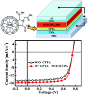
We reported a significant improvement in the efficiency of polymer solar cells by introducing C60 pyrrolidine tris-acid (CPTA) to modify the interface between inorganic TiO2 nanorods and the organic active layer. The devices with CPTA-modified TiO2 as the cathode buffer layer exhibited a power conversion efficiency (PCE) as high as 8.74%, accounting for a 12.8% enhancement compared with the bare TiO2 based devices (7.75%) in the polymer thieno[3,4-b] thiophene/benzodithiophene:[6,6]-phenyl C71-butyric acid methyl ester (PTB7:PC71BM) system. We found that the CPTA layer improves the surface properties of the bare TiO2 film so that charge transfer between the active layer and the TiO2 layer is enhanced.
Titanium dioxide (TiO2) has been extensively studied as an n-type semiconductor owing to high electron mobility, good transparency and nontoxic.8,11,12,20 Over the past decades, TiO2 has been widely applied in dye-sensitized solar cells (DSSCs),21 photocatalysis,22 and hybrid organic solar cells.23,24 It has been demonstrated that TiO2 can effectively help to collect electrons and block holes.13,25,26 To further enhance the device performance, the interfacial modification of TiO2 which enhances the compatibility and adhesion between the inorganic metal oxide and organic active layer has drawn considerable attention.16,26,27 For example, a C60 derivative functionalized with a carboxylic acid group, which can form a self-assembled monolayer (SAM) on the metal oxide surface, has been used successfully to simultaneously improve the morphology and charge selectivity of the inverted devices.28,29 It is believed that interfacial modification by inserting an additional C60 derivative interlayer between the organic active layer and the inorganic metal oxide could help to enhance device performance.27,29–31
In this work, we introduced a polar fullerene derivative with carboxyl groups, C60 pyrrolidine tris-acid (CPTA), between the organic active layer and anatase titania nanorods (NRs) (Fig. 1a) to improve the device performance. This is expected to improve the charge transport and charge collection in PSCs as well as reduce charge recombination probability. CPTA is soluble in methanol because of the polar property of carboxyl groups. It was reported that CPTA used as a cathode buffer layer has an excellent electron-collecting and hole-blocking ability.32 Low bandgap polymer thieno[3,4-b]-thiophene/benzodithiophene (PTB7) was used as the donor and phenyl C71-butyric acid methyl ester (PC71BM) was used as the acceptor. A high performance device was fabricated with the inverted configuration ITO/TiO2/CPTA/PTB7:PC71BM/MoO3/Al (Fig. 1a). For comparison, the reference device (without CPTA layer) was also made under the same conditions. As a result, the inverted device based on an ITO/TiO2/CPTA/PTB7:PC71BM/MoO3/Al configuration exhibited an enhanced PCE of 8.74% in comparison to the reference device (PCE = 7.75%) without CPTA interlayer.
![]() | ||
Fig. 1 (a) The device structure of the inverted PSC. (b) The molecular structures of CPTA and PC71BM. |
Fig. 2 shows the energy levels diagram of the materials involved in the inverted device. The details of anatase TiO2 synthesis are described in the ESI† and the dimensions of TiO2 NRs were ∼35–45 nm in length and 3–5 nm in diameter as shown in TEM image (Fig. S1†). The lowest unoccupied molecular orbital (LUMO) and highest occupied molecular orbital (HOMO) of TiO2 are located at 4.1 eV and 7.3 eV, respectively.33 The higher LUMO energy level of CPTA has been reported to be 3.94 eV, which was located between the LUMO of PC71BM (3.69 eV) and the conduction band of TiO2 (4.1 eV).32 From the energy levels diagram (Fig. 2), it is clear that CPTA functions as an intermediate in the energy gradient. Therefore, electrons in the PC71BM domain can be efficiently extracted by CPTA and transported to the TiO2 through an energetically favorable pathway. In addition, the HOMO of CPTA is low-lying relative to the HOMO of PC71BM, which would efficiently block the holes and reduce the recombination at the interfaces.
The current density versus voltage (J–V) characteristics of inverted PSCs obtained under 100 mW cm−2 AM 1.5G illumination are shown in Fig. 3a. Table 1 summarized the specific parameters of devices A (ITO/TiO2/PTB7:PC71BM/MoO3/Al) and B (ITO/TiO2/CPTA/PTB7:PC71BM/MoO3/Al). The device A without CPTA layer showed an open circuit voltage (Voc) of 0.758 V, a short current density (Jsc) of 14.69 mA cm−2, a fill factor (FF) of 69.6% and a PCE of 7.75%. When CPTA was inserted between TiO2 and active layer, the Jsc and FF were enhanced significantly. The device B with an optimized concentration 0.5 mg ml−1 (see Table S1 in the ESI†) exhibited an impressive improved PCE of 8.74%, which was enhanced 12.8% compared with the device A (7.75%). The device B showed a higher Jsc and FF than device A, indicating that CPTA could efficiently extract and transport the electron to the TiO2 through an energetically favorable pathway, which can be proved by the obvious decrease of series resistance (Rs) from 5.24 Ω cm2 (device A) to 3.88 Ω cm2 and the increased shunt resistance (Rsh) of 1021 Ω cm2 (device A) from 1567 Ω cm2 (Table 1). It indicated better interface property in the device B, which will lead to more efficient electron transport, collection and less charge carrier recombination at the TiO2 interface. The external quantum efficiency (EQE) (see Fig. 3b) of devices B was much higher at almost whole wavelength range compared with that of devices A. It further confirmed that using organic CPTA to modify inorganic TiO2 interface was an efficient method to improve the device performance for the inverted PSCs.
Devicea | Voc [V] | Jsc [mA cm−2] | FF (%) | ηb (%) best (average) | Rs [Ω cm2] | Rsh [Ω cm2] |
---|---|---|---|---|---|---|
a Configurations: device A, ITO/TiO2/PTB7:PC71BM/MoO3/Al; device B, ITO/TiO2/CPTA/PTB7:PC71BM/MoO3/Al.b Average of eight devices. The device parameter distribution maps are presented in Fig. S2 in the ESI. | ||||||
A | 0.758 | 14.69 | 69.6 | 7.75 (7.56 ± 0.19) | 5.24 | 1021 |
B | 0.757 | 15.73 | 73.5 | 8.74 (8.45 ± 0.20) | 3.88 | 1567 |
Fig. 4a and b exhibit the atomic force microscopy (AFM) tapping mode height images (5 × 5 μm) of the surface of bare TiO2 and TiO2/CPTA on ITO substrate, respectively. In the case of bare ITO/TiO2 sample, the image showed a root mean square (RMS) roughness of 4.85 nm. After a layer of CPTA was deposited on top of bare ITO/TiO2, the RMS roughness decreased to 4.03 nm. The decreased surface roughness reveals that voids in the uneven TiO2 NRs surface are filled and covered by the CPTA to form a smoother surface. The result suggests that the CPTA modification would vary the morphology of the bare TiO2 film, which would further affect the morphology of the active layer. Water contact angle measurements were further performed for bare TiO2 film and the TiO2/CPTA film, as shown in Fig. 4c and d. The bare TiO2 film exhibited a water contact angle of 84.1°, which could be due to the oleic acid and pyridine attaching on TiO2 NRs surface.34 The wetting contact angle of the CPTA-modified TiO2 film was further increased to 99.2° from 84.1° (bare TiO2 film). The increased hydrophobicity could be mainly attributed to the intrinsic hydrophobicity of fullerene unit in the CPTA molecule. Owing to the hydrophobic organic solvent (chlorobenzene) used in the deposition of the active layer, the enhanced hydrophobicity of buffer layer would help the flow and the spread of the active layer solution to deposit on the buffer layer.10,26,30,35 Consequently, CPTA modification of the bare TiO2 surface can help to improve the morphology of the active layer and provide a better percolation conduction pathway at the interface.28 The improved interface properties could also reduce the recombination of charge carriers and contact resistance, improving charge transfer at the interface and leading to better device performance.26,36
![]() | ||
Fig. 4 (a) AFM images (5 × 5 μm) of bare TiO2 and (b) TiO2/CPTA. Contact angle images by dropping deionized water on the surface of bare TiO2 (c) and TiO2/CPTA (d). |
In conclusion, the inverted PSCs were fabricated by using TiO2 NRs and CPTA-modified TiO2 NRs as the cathode buffer layer. We found that modification of the interface between the inorganic TiO2 NRs and organic active layer with a fullerene derivative (CPTA) can improve the device performance. The devices with CPTA modifier on the TiO2 NRs surfaces lead to a significant improvement compared with bare TiO2. A high PCE of 8.74% was achieved, which was enhanced 12.8% compared with the bare TiO2 based devices (7.75%). The CPTA layer improves surface property of the bare TiO2 film so that the modified TiO2 film has lower contact resistance, improved charge transfer and better adhesion with the active layer. We believe that this study will stimulate further research on understanding how to improve the interface, enhance charge transfer properties and achieve better device performance in inverted PSCs.
Footnote |
† Electronic supplementary information (ESI) available: Specific devices parameters based on TiO2 NRs modified with the different concentrations of CPTA in PTB7:PC71BM blends, the device parameters distribution map using TiO2 NRs and TiO2 modified with CPTA as buffer layer in PTB7:PCB71M system. See DOI: 10.1039/c4ra02254h |
This journal is © The Royal Society of Chemistry 2014 |