Earth-abundant and low-cost CZTS solar cell on flexible molybdenum foil†
Yongzheng Zhangab,
Qinyan Yeb,
Jiang Liub,
Hao Chenb,
Xulin Heb,
Cheng Liao*b,
Junfeng Hanb,
Hao Wanga,
Jun Meib and
WoonMing Laub
aThe College of Materials Science and Engineering, Beijing University of Technology, Beijing 100124, PR China
bChengdu Green Energy and Green Manufacturing Technology R&D Centre, Southwest Airport Economic Development Zone, Shuangliu, Chengdu, 610207, P. R. China. E-mail: cliao315@hotmail.com; Fax: +86-28-67076210; Tel: +86-28-67076209
First published on 15th May 2014
Abstract
Flexible Cu2ZnSnS4 (CZTS) solar cell absorbers were prepared by sulfurizing Cu–Zn–Sn precursors which were co-electrodeposited on Mo-coated molybdenum foil in a one-step process. A photovoltaic device with 3.82% conversion efficiency based on the illumination area of 0.35 cm2 was attained, which is the first efficiency report of flexible CZTS-based solar cells on molybdenum foil.
Thin film solar cells based on copper zinc tin sulfide (Cu2ZnSnS4, CZTS) have demonstrated significant improvements over recent years.1–4 It is regarded as a promising candidate for next generation PV materials because of its high theoretical efficiency, low-cost potential and environmental friendliness. These advantages are based on its large absorption coefficients (>104 cm−1), ideal direct band-gap (1.45 eV) and its earth-abundance, as well as being almost free of rare or toxic elements. The best CZTS solar cell (pure sulfide) so far, reaching 8.4% power conversion efficiency, is produced on rigid glass substrate by vacuum thermal evaporation process.5 However, solar cells on flexible substrates seem more attractive for their applications on both ground and space utilities due to its high power/mass (W kg−1) ratio, as well as further cost reduction by roll-to-roll deposition method.6,7
The most commonly used flexible substrates are metal foils (e.g., stainless steel, aluminum, or molybdenum) and organic films (e.g., polyimide).8 However, the maximum sustainable temperature of polyimide (PI), typically below 500 °C, is much lower than that of metal foils, which can withstand temperature of up to 600 °C or even higher. Metal foils possess some distinct advantages not only in the higher temperature resistance but also in the mechanical strength over PI.9,10 Particularly, the high conductivity of metal foils substrate contributes to electrochemical deposition method, which is one of the best choices of low cost, low energy consumption and roll-to-roll production.11 Among these kinds of metal foils, molybdenum is the first choice for its compatible coefficient of linear thermal expansion (linear CTE), 5.2 × 10⁻⁶ K−1.12 Besides, high purity molybdenum foil does not need the barrier layers in cell structure, whereas other substrates such as stainless steel contains some deep level impurities like Fe, which adversely affects the electronic properties of absorbers.13
In this work, we report an approach to fabricate CZTS films on commercial molybdenum foil by electrochemical deposition. After the CZTS device was finished with a structure of Mo foil/Mo film/CZTS/CdS/ZnO/Al:ZnO/Al, an efficiency of 3.82% with device area of 0.35 cm2 is attained. To our best knowledge, this is the first report of flexible CZTS-based solar cells on molybdenum foil.
Molybdenum foil (0.5 mm thick, 99.95% purity) was potentiostatically polished at 6 V (vs. Ag/AgCl) at room temperature for 1.5 min in 87.5 ml methanol and 12.5 ml sulfuric acid mixed solution. The surface morphology of post-polished molybdenum foil was analyzed using atomic force microscopy (AFM) as shown in Fig. S1 (see ESI†). Then, 800 nm thick Mo back contacts were deposited by DC sputtering (sheet resistance 0.2–0.3 Ω per square). The Cu–Zn–Sn precursors were electrodeposited in one-step process by differential pulse voltammetry method. A three-electrode system was used with Mo coated molybdenum foil as working electrode, a platinum (Pt) gauze as counter electrode and Ag/AgCl as reference electrode. Analytical reagent grade chemicals (Sigma-Aldrich) were used for the electrolytic bath preparation. The electrolyte contained 4 mM CuSO4, 3 mM ZnSO4, and 3 mM SnSO4 without complexing agent. The CZTS absorber layers were prepared by rapid thermal processing (RTP) the Cu–Zn–Sn precursors at 550 °C in a quartz tube filled with a 30 Torr of 5% H2S (in N2) for 1 h. The rest of the device structure consists of 80–100 nm CdS by chemical bath deposition, ∼80 nm i-ZnO/∼600 nm Al-doped ZnO by RF magnetron sputtering and Ni–Al metal grids. Finally, a mechanical scribing step defined the cell area to 0.35 cm2.
It can be seen from the cross-sectional SEM image of the precursors in Fig. 3(a) that a “flower-like” structure of Cu–Zn–Sn alloys, assembled by nano-metals with the size of approximate 40 nm, was prepared. This “flower-like” structure tends to form homogeneous CZTS films more efficiently than ordinary structures during annealing.
After being annealed at 550 °C for 1 h in H2S atmosphere, the phase of the CZTS film were determined by XRD and Raman. Fig. 1(a) shows the XRD patterns of the CZTS absorber layer, exhibiting the main diffraction peaks of kesterite CZTS (JCPDS# 26-0575), with the lattice constants a = b = 5.427 Å and c = 10.848 Å. The sharp peaks indicate a relatively large grain size and good crystallization. The sputtered Mo (JCPDS# 42-1120) exhibits (110) crystal orientation compared to the molybdenum foil (JCPDS# 42-1120) (200), (211), which are labeled in the XRD patterns. Due to very similar lattice parameters or analogous pattern features for cubic ZnS, tetragonal Cu2SnS3 and kesterite CZTS, Raman spectroscopy was used to further distinguish the CZTS phase and other secondary phases. The Raman spectra shown in Fig. 1(b) verify the good purity of the kesterite CZTS phase more concretely, with the characteristic peaks at 287, 338, 368 cm−1, in good agreement with well-known vibrational characteristics of CZTS material.14,15
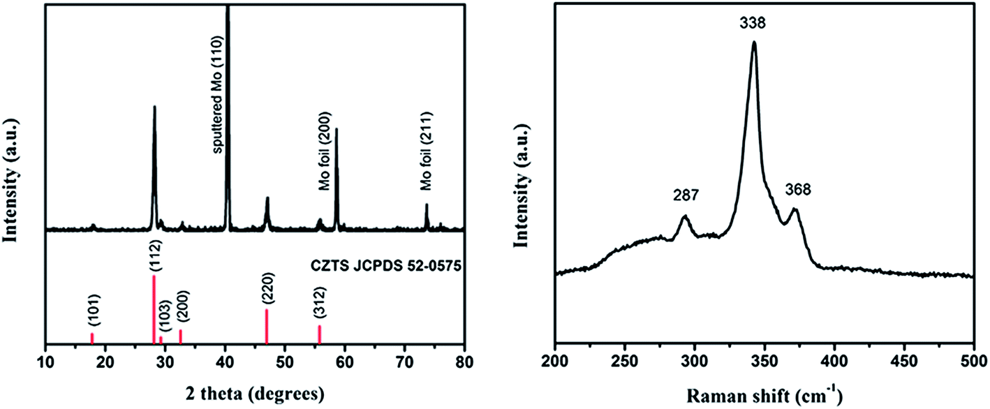 | ||
| Fig. 1 XRD patterns (a) and Raman spectra (b) of CZTS film. | ||
In order to determine the photoelectric properties of the CZTS films, photoelectrochemical (PEC) measurements were carried out as shown in Fig. 2. A sharp and rapid current response arose when light was turned on, indicating that the CZTS film is sensitive to photons injection. The respectable signal at 0 V also shows the light generated charge carriers have relatively long diffusion lengths (or lifetimes) to be collected without the assistance of CZTS/buffer built-in field or additional bias. This result implies the electron–hole recombination is well suppressed, which is attributed to good quality of CZTS absorber film with high crystallization and few secondary phases.
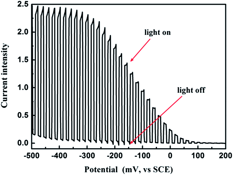 | ||
| Fig. 2 Linear sweep voltammograms (LSVs) of the CZTS film. | ||
Fig. 3(b) presents a cross-sectional SEM image of our CZTS solar cell. The cross-section EDS elemental profiles determined from line scan and elemental mapping images are shown in Fig. 3(c)–(f), respectively. However, conventional EDS is not capable of providing quantification for the content of S due to the fact that the X-ray emission lines of Mo and S are superimposed. The X-ray emission lines are 2.29 keV for the Mo Lα line and 2.30 keV for the S Kα line. So in this case, we deducted Mo and S content and only determined Cu, Zn, Sn, and Cd. It can be learned in Fig. 3(b) that the metal elements are distributed homogeneously across the cross-section region, which indicates there is few secondary phases such as Cu3SnS4 and ZnS formed during the preparation of CZTS film. On the basis of elemental profiles determined from EDS line scan as shown in Fig. 3(c), we can learn that the fluctuation of homogeneity throughout the bulk of the film is tiny. The ratios of Cu/Zn + Sn and Zn/Sn calculated from Fig. 3(c) are 0.82–0.85 and 1.2–1.3, respectively, yielding Cu-poor and Zn-rich compositions. The grain nucleation and growth of CZTS films out of initially Cu-poor and Zn-rich environments, just like the case in this work, is significant to the formation of intrinsic defects, including VCu vacancies, ZnCu antisites and derivative defect clusters. These intrinsic defects act as shallow acceptors and show p-type conductivity, according to some works based on first principle calculations.16
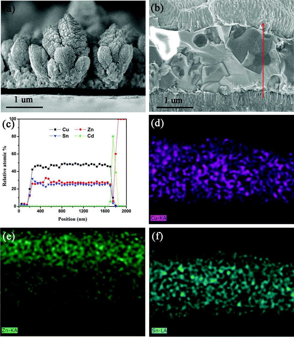 | ||
| Fig. 3 (a) Cross section of Cu–Zn–Sn precursors on molybdenum foil; (b) cross section of CZTS film with corresponding EDS line scan (c) taken along the red line; mapping images of Cu (d), Zn (e), Sn (f). | ||
Table 1 shows the characteristics of other devices and Fig. 4 shows the J–V characteristics for the best flexible CZTS solar cell under AM1.5G illumination. The best device represents a power conversion efficiency (PCE) of 3.82% with the illumination area of 0.35 cm2, which is the first efficiency report of flexible CZTS based solar cells on molybdenum foil so far. The device gives an open circuit voltage of Voc = 473 mV and photocurrent of Jsc = 18.84 mA cm−2 where the fill factor (FF) is 42.90%. The present CZTS cell has relatively lower Jsc and higher Voc, compared with our previous work.17 The PCE may be limited by a high series resistance (4.64 Ω cm2), resulting in a substantial loss in fill factor. It is expected that a significant improvement in device performance could be achieved by improving the sheet resistances of the Mo and AZO layers. In addition, the interface defects or bulk defects near the CZTS/CdS heterojunction would impact the carrier lifetime, which cause the decrease of Voc significantly. Besides, reflection by the metal contacts or the active area of the device, as well as absorption of CdS buffer layer and transparent conducting oxide layer, could decrease Jsc.
| Cell | Voc/mV | Jsc/mA cm−2 | FF/% | Rs/Ω cm2 | Eff./% |
|---|---|---|---|---|---|
| D1 | 497 | 15.05 | 46.3 | 4.32 | 3.46 |
| D2 | 442 | 15.56 | 38.9 | 6.23 | 2.68 |
| D3 | 422 | 11.87 | 47.4 | 4.40 | 2.37 |
| D4 | 454 | 11.03 | 42.3 | 4.87 | 2.12 |
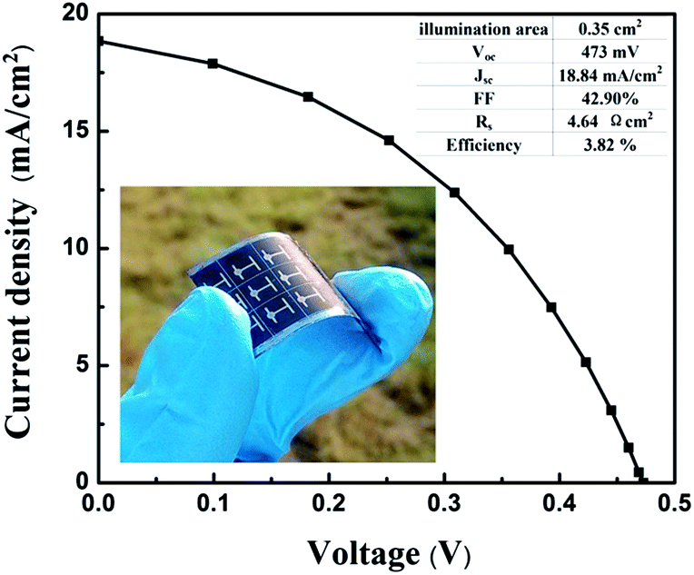 | ||
| Fig. 4 J–V curve of the best CZTS solar cell measured under a simulated AM1.5G illumination. The inset is photograph of a sample on molybdenum foil with single cells. | ||
The external quantum efficiency (EQE) curve of the corresponding ZnO/CdS/CZTS heterojunction solar cell is presented in Fig. 5. The EQE starts slowly at about 400 nm due to the cut-off of CdS buffer layer and ZnO window layer. The quantum efficiency reaches a maximum value of 82.9% at 575 nm. However, it drops off significantly in the near IR range and ends around 900 nm, which is related to optical absorption of the CZTS absorber. The dotted line inserted is the derivative of EQE as a function of wavelength, which is used to estimate the effective band gap of the absorbers. Peak at 820 nm is observed in the dotted curve, corresponding to absorption edges of CZTS films. According to the inverse correlation between photon energy and wavelength, the band gap of CZTS absorber can be calculated to be 1.51 eV from the peak at 820 nm. Assuming there is no optical and electrical loss from ZnO or CdS layers, and 100% quantum efficiency is attained between 350 nm and 510 nm, the Jsc would rise to 25.2 mA cm−2, which is still far lower than the typical Jsc of the CZTSe solar cell (∼35 mA cm−2). Although the open-circuit voltage is higher than most CZTSe cells, which have wider band gaps, the value of Voc does not increase proportionally with the increase of the band-gap energy, thus decreasing the conversion efficiency as compared with our previous results. Achieving a higher efficiency appears to be limited by a Voc deficit and low fill factor in addition to a rather high series resistance of 4.64 Ω cm2. Besides, broadening the spectrum absorption range by decreasing the absorber band-gap and simultaneously maintaining the existing Voc would help to improve efficiency. Improvements in device performance are expected with further studies by optimization of the absorber band-gap with Se partly replacing S.1 Thinning the thickness of CdS and TCO layers and increasing CZTS layer to make sure the maximizing the light transmission into the CZTS absorber layer is also a way to increase Jsc.3
 | ||
| Fig. 5 External quantum efficiency (EQE) curve of ZnO/CdS/CZTS heterojunction solar cell. The insert is the derivative of EQE as a function of wavelength. | ||
In summary, we report a method to fabricate CZTS solar cells on flexible molybdenum foil with power conversion efficiency of 3.82% based on the illumination area of 0.35 cm2. From the data of EQE, Further optimization of synthesis and device fabrication would lead to enhanced efficiency and a high power/mass ratio route to earth-abundant elements, low-cost, widely-used thin film solar cells. However, further improvement requires extensive systematic investigations to optimize the involved layers and processing conditions.
Acknowledgements
This work is supported by the National Nature Science Foundation of China (51202227), the Synergistic Innovative Joint Foundation of AEG-SCU (xtcx2011008) and the National High Technology Research and Development Program of China (2012AA050704).References
- W. Wang, M. T. Winkler, O. Gunawan, T. Gokmen, T. K. Todorov, Y. Zhu and D. B. Mitzi, Adv. Energy Mater., 2014, 4 DOI:10.1002/aenm.201301465
.
- K. Ramasamy, M. A. Malik and P. O'Brien, Chem. Commun., 2012, 48, 5703 RSC
- M. T. Winkler, W. Wang, O. Gunawan, H. J. Hovel, T. K. Todorov and D. B. Mitzi, Energy Environ. Sci., 2014, 7, 1029–1036 CAS
- A. Polizzotti, I. L. Repins, R. Noufi, S.-H. Wei and D. B. Mitzi, Energy Environ. Sci., 2013, 6, 3171–3182 CAS
- B. Shin, O. Gunawan, Y. Zhu, N. A. Bojarczuk, S. J. Chey and S. Guha, Prog. Photovoltaics, 2013, 21, 72–76 CAS
- A. Chirila, S. Buecheler, F. Pianezzi, P. Bloesch, C. Gretener, A. R. Uhl, C. Fella, L. Kranz, J. Perrenoud, S. Seyrling, R. Verma, S. Nishiwaki, Y. E. Romanyuk, G. Bilger and A. N. Tiwari, Nat. Mater., 2011, 10, 857–861 CrossRef CAS PubMed
- N. G. Dhere, Sol. Energy Mater. Sol. Cells, 2007, 91, 1376–1382 CrossRef CAS PubMed
- F. Kessler and D. Rudmann, Sol. Energy, 2004, 77, 685–695 CrossRef CAS PubMed
- D. Rudmann, D. Brémaud, H. Zogg and A. Tiwari, J. Appl. Phys., 2005, 97, 084903 CrossRef PubMed
- R. Caballero, C. A. Kaufmann, T. Eisenbarth, T. Unold, R. Klenk and H. W. Schock, Prog. Photovoltaics, 2011, 19, 547–551 CAS
- A. Kampmann, J. Rechid, A. Raitzig, S. Wulff, M. Mihhailova, R. Thyen and K. Kalberlah, Mater. Res. Soc. Symp. Proc., 2003, 763, 323–328 CAS
- M. Patel and A. Ray, Phys. B, 2012, 407, 4391–4397 CrossRef CAS PubMed
- K. Herz, A. Eicke, F. Kessler, R. Wächter and M. Powalla, Thin Solid Films, 2003, 431, 392–397 CrossRef
- A. Shavel, D. Cadavid, M. Ibáñez, A. Carrete and A. Cabot, J. Am. Chem. Soc., 2012, 134, 1438–1441 CrossRef CAS PubMed
- E. Thimsen, S. C. Riha, S. V. Baryshev, A. B. F. Martinson, J. W. Elam and M. J. Pellin, Chem. Mater., 2012, 24, 3188–3196 CrossRef CAS
- S. Chen, A. Walsh, X. G. Gong and S. H. Wei, Adv Mater, 2013, 25, 1522–1539 CrossRef CAS PubMed
- Y. Zhang, C. Liao, K. Zong, H. Wang, J. Liu, T. Jiang, J. Han, G. Liu, L. Cui, Q. Ye, H. Yan and W. Lau, Sol. Energy, 2013, 94, 1–7 CrossRef CAS PubMed
Footnote |
| † Electronic supplementary information (ESI) available. See DOI: 10.1039/c4ra02064b |
| This journal is © The Royal Society of Chemistry 2014 |