Performance of a nanoarchitectured tin oxide@reduced graphene oxide composite as a shield against electromagnetic polluting radiation
Monika Mishraa,
Avanish Pratap Singha,
Bhanu Pratap Singhb and
S. K. Dhawan*a
aPolymeric & Soft Materials Section, CSIR-National Physical Laboratory, Dr K. S. Krishnan Road, New Delhi-110 012, India. E-mail: skdhawan@mail.nplindia.ernet.in; Fax: +91-11-25726938; Tel: +91-11-45609401
bPhysics and Engineering of Carbon, CSIR-National Physical Laboratory, Dr K. S. Krishnan Road, New Delhi-110 012, India
First published on 23rd May 2014
Abstract
Tin oxide nanoparticles architectured with a reduced graphene oxide composite (SnO2@RGO) have been synthesised by in situ reduction of graphene oxide in the presence of stannous chloride. The microwave shielding performance of SnO2@RGO has been evaluated over the X-band (8.2–12.4 GHz) range. XRD and TEM studies show that the tin oxide nanoparticles are anchored uniformly onto the surface of the reduced graphene oxide sheets. A total electromagnetic interference shielding effectiveness in the order of 62 dB was achieved, which is more than the required values (∼30 dB) desired for techno-commercial applications.
1. Introduction
Graphene and graphene-based composites with electroconductive properties are very promising materials for numerous uses in technological applications, such as energy storage,1 electro-optical devices,2,3 and electromagnetic shielding.4,5 With the rapid growth of the electronics industry, most communication devices have shifted towards a higher frequency range. For abundant electrical and electronic devices, electromagnetic interference (EMI) remains a technical task in terms of the proper matching of impedance. EMI tends to reduce the response in the performance of the equipment. The shielding of various electronic devices from mobile signals and EMI is important, and this is performed by microwave shielding materials.6,7 Most of the electromagnetic shields are ferrites,8–10 metallic magnetic materials,11–14 and carbon nanotube (CNT) composites.15–17 Usually, metals are used for this purpose, but the layers commonly stumbled upon in metal sheets tend to cause radiation seepages, which lessen the effectiveness of the shielding material. Graphene matrix composites that contain conductive fillers are most promising EMI-shielding materials.18,19 Impedance matching, defect polarization relaxation and electronic dipole relaxation are present in reduced graphene oxide, which help to improve electromagnetic shielding.20 Thus, reduced graphene oxide shows improved microwave shielding when compared with graphite and carbon nanotubes and is likely to show better absorption than that compared to high quality graphene, making it a promising candidate as a microwave shielding material.21–23 Our previous efforts based on graphene encourage us to search more and more for new types of composites of graphene.4,24–26 The present investigation is one of the most innovative efforts to discover new types of material for EMI shielding.Recent advances in architecting graphene with different materials such as Fe3O4,25 TiO2 (ref. 27) and gold nanoparticles28 inspire us to design SnO2 decorated reduced graphene oxide (RGO) sheets. RGO–SnO2 composites have attracted significant attention recently due to their potential applications.29,30 The combination of the high conductivity of the RGO sheets and tin oxide nanoparticles make it a constructive candidate for the next generation of microwave absorbing materials. Special attention is dedicated to reducing the reinforced particle size and allowing environmentally friendly synthesis conditions. Small, as low as 3–5 nm, average crystallite sizes have already been reported.31,32 Moreover, small size particles possess high anisotropy energy, which also contributes in the enhancement of their microwave shielding properties.
In this study, we attempt to architect RGO sheets using tin oxide nanoparticles via an in situ reduction of graphene oxide (GO) in the presence of stannous chloride and hydrochloric acid, for high-performance EMI shielding applications. The facile method used in this study has several advantages over traditional GO reduction methods such as an extra reducing agent e.g. hydrazine hydrate is not required for the reduction of GO to RGO and the in situ genesis of nanoparticles leads to uniform size particles on individual RGO sheets. Such architectured SnO2 decorated RGO sheets exhibit enhanced shielding effectiveness when compared to conventional EMI shielding materials. The resulting composite possesses high dielectric properties with moderate conductivity, making it a next-generation material for use in EMI shielding against electromagnetic pollution. The intended composite is promising and light-weight for a practical use of EMI shielding applications in the areas of stealth technology.
2. Experimental section
2.1 Materials
Natural graphite powder (purity 99.5%, particle size 50 μm) procured from Loba Chemie, India, has been used to synthesize GO. Stannous(II) chloride dihydrate (SnCl2·2H2O) and NaNO3 were obtained from Qualigens Fine Chemicals, India; HCl from Rankem, India; ammonia and KMnO4 from Fisher scientific, India; and H2SO4 and ethanol were obtained from Merck, India. Double distilled water with a specific resistivity of 106 Ω cm was used for preparing aqueous solutions and for filtration purposes.2.2 Preparation of materials
A typical preparation process for SnO2 decorated RGO is as follows: 14 g of SnCl2·2H2O was added to 500 mL HCl solution (100 mL L−1 of 37 wt% HCl). Then, this solution was mixed with the GO solution and sonicated for 1 h. The resulting mixture was stirred at 90 °C for 6 h. SnO2@RGO was collected after several washings with water through centrifugation, then dried in a vacuum oven at 100 °C. Calcination (400 °C for 5 h under a N2 atmosphere) was carried out to improve the crystallity of SnO2.31 The possible reaction mechanism can be written as follows:
| SnCl2·2H2O + GO + H2O + 2HCl → SnO2@RGO |
A schematic representation of RGO decoration using SnO2 nanoparticles is shown in Fig. 1a.
 | ||
| Fig. 1 (a) A schematic representation of the architectured SnO2 nanoparticles on the surface of the RGO sheets, (b) TEM images of the SnO2 nanoparticles at different magnifications and (c) TEM images of the as-synthesized SnO2@RGO composite. | ||
2.3 Materials characterization
The morphology of the RGO–SnO2 composites was characterized by transmission electron microscopy (TECNAI G2T30, u−TWIN) at an acceleration voltage of 300.0 kV. X-ray diffraction (XRD) measurements were performed on a D8 Advance XRD (Bruker) using CuKα radiation (λ = 1.54 Å) in the scattering range (2θ) of 10°–80° with a scan rate of 0.02° s−1 and slit width of 0.1 mm. FT-IR spectra were recorded on a Nicolet 5700 spectrometer in transmission mode in the wave number range of 400–4000 cm−1. Spectroscopic grade KBr pellets were used for collecting the spectra with a resolution of 4 cm−1 performing 32 scans. Raman analysis was carried out using a Renishaw inVia Reflex spectrometer, UK with an excitation source of 514.5 nm. The resolution of the instrument was less than 1.0 cm−1. The dc electrical conductivity has been measured using a standard four-probe technique, in order to eliminate contact resistance effects, using a Keithley programmable current source (model 6221) and nano voltmeter (model 2182A). Electromagnetic shielding and dielectric measurements have been carried out using an Agilent E8362B Vector Network Analyzer in the 8.2–12.4 GHz (X-band) microwave range. The composite has compacted in a piston cylinder assembly at 60 MPa for 5 min into different thickness rectangle pellets with a dimension to fit the waveguide dimensions.3. Results and discussion
3.1 Morphological analysis
Fig. 1b and c demonstrate the transmission electron microscopy (TEM) images of the SnO2 nanoparticles and SnO2 decorated RGO. Fig. 1b shows the SnO2 nanoparticles at different magnifications. Higher magnification images (Fig. 1b1 and 1b2) confirm that all particles are of 3–5 nm diameter. It is evident that the RGO sheet was uniformly decorated by a large quantity of SnO2 nanoparticles, and the outline of both RGO and SnO2 nanoparticles can be clearly seen as depicted in Fig. 1c. Higher magnification images (Fig. 1c2 and 1c3) revealed that the SnO2 nanoparticles have grown on the surface of the RGO sheet and were distributed over the RGO's surface. SnO2 nanoparticles can exist densely on both sides of these sheets. Most importantly, there are no vacant areas on the RGO sheets that are not decorated with SnO2 nanoparticles. It is worthy to notice that these SnO2 nanoparticles are strongly attached to the RGO sheets, because sonication was applied during the preparation of the TEM samples, indicating excellent bonding between the RGO and SnO2 nanoparticles. The presence of dielectric nanoparticles on a conducting surface is helpful for enhancing the shielding properties of the material.3.2 Structural analysis
The crystal structure of GO, RGO and RGO–SnO2 was characterized by XRD and the results displayed in Fig. 2a. The powder X-ray diffraction pattern of GO shows a diffraction peak around 10.2°, which corresponds to the (002) reflection of the stacked GO sheets. It shows an interlayer spacing of 0.86 nm for GO, which is more than graphite with an interlayer spacing of 0.34 nm. It is due to the introduction of oxygen containing groups on the GO sheets. Chemical reduction of GO to RGO leads to broadening and shifting of the XRD peak to around 24.9° corresponding to an interlayer spacing of about 0.36 nm. This indicates the presence of residual oxygenated groups on the RGO sheets. For SnO2@RGO, there are no diffraction peaks corresponding to GO, indicating the reduction of GO to RGO by stannous ions. The diffraction patterns and relative intensities of the synthesized SnO2 matched well with standard SnO2 (JCPDS 41-1445), demonstrating that the nanoparticles were SnO2 and shows that the diffraction peaks of crystalline SnO2 nanoparticles are clearly distinguishable. It could be indexed to the tetragonal SnO2 phase (JCPDS 41-1445). The XRD peaks of the composite appearing at about 2θ = 26.5, 33.9, and 51.6 can be indexed to the diffraction planes of SnO2 (110), (101), and (211), respectively. The mean particle size (D) of the SnO2 nanoparticles was calculated by applying the Scherrer equation to the (110) plane diffraction peak and found to be 3–5 nm in the SnO2@RGO composite.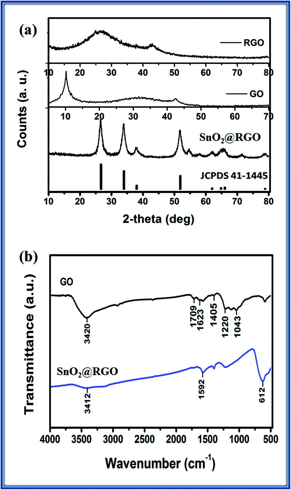 | ||
| Fig. 2 (a) X-ray diffraction patterns of SnO2@RGO, GO and RGO (b) comparison of the FT-IR spectra of the GO and SnO2@RGO composite. | ||
3.3 FT-IR spectroscopy
Fig. 2b shows the FT-IR spectra of GO and SnO2@RGO. The FT-IR spectra of GO confirmed the presence of oxygen-containing groups, such as C–OH at 3420 cm−1, C–O–C at 1220 cm−1, and C![[double bond, length as m-dash]](https://www.rsc.org/images/entities/char_e001.gif) O in the carboxylic acid moieties at 1709 cm−1. Other characteristic vibrations were the O–H deformation peak at 1405 cm−1 and the C–O stretching peak at 1043 cm−1. The peak at 1623 cm−1 was assigned to the contributions from the skeletal vibrations of the graphitic domains. For SnO2@RGO, the carboxylic acid vibration band at 1709 cm−1 disappeared. A weak signal for the C–OH stretching vibration at 3412 cm−1 could be ascribed to the vibrations of the adsorbed water molecules which is assigned to the Eu mode of SnO2 (antisymmetric O–Sn–O stretching). The presence of the Eu mode (a band located at 612 cm−1) in SnO2@RGO indicates the incorporation of SnO2 particles on the RGO sheets. Additionally, the spectrum of the SnO2@RGO composite shows an absorption band at 1592 cm−1 (CC stretching), indicating the restoration of the graphene network on reduction. Therefore, it could be concluded that GO was reduced by the stannous ions.
O in the carboxylic acid moieties at 1709 cm−1. Other characteristic vibrations were the O–H deformation peak at 1405 cm−1 and the C–O stretching peak at 1043 cm−1. The peak at 1623 cm−1 was assigned to the contributions from the skeletal vibrations of the graphitic domains. For SnO2@RGO, the carboxylic acid vibration band at 1709 cm−1 disappeared. A weak signal for the C–OH stretching vibration at 3412 cm−1 could be ascribed to the vibrations of the adsorbed water molecules which is assigned to the Eu mode of SnO2 (antisymmetric O–Sn–O stretching). The presence of the Eu mode (a band located at 612 cm−1) in SnO2@RGO indicates the incorporation of SnO2 particles on the RGO sheets. Additionally, the spectrum of the SnO2@RGO composite shows an absorption band at 1592 cm−1 (CC stretching), indicating the restoration of the graphene network on reduction. Therefore, it could be concluded that GO was reduced by the stannous ions.
3.4 Raman spectroscopy
Raman spectroscopy is a very powerful tool for investigating the interactions or bonding between two components.33 To elucidate the graphitic structure of GO, RGO and the interactions among RGO, and SnO2 nanoparticles, Raman spectroscopy was conducted in a spectral range of 100–3300 cm−1. Fig. 3 shows the Raman spectra of GO, RGO, and SnO2@RGO composite. The Raman spectra of GO and RGO consist of three prominent characteristic peaks, namely the D band (disorder-induced band), the G band (the tangential mode of graphitic structure), and the G′ (or 2D) band. The G and D bands are due to the doubly degenerate zone centre E2g mode (∼1580–1600 cm−1) and the breathing modes of six atom rings which appears at ∼1350 cm−1 due to the presence of defects in the graphite, respectively.34 In the Raman spectrum of RGO, the D, G and 2D peak position values confirm the formation of RGO. Raman spectrum of pure SnO2 nanoparticles reveals all the characteristic bands of SnO2 in the low frequency region, i.e., 436, 479 (Eg), 564 (S1), 633 (A1g).35 All these peaks are suppressed in the SnO2@RGO composite because of the highly intense graphitic peaks present in the RGO sheets. Furthermore, the interactions between the RGO and SnO2 nanoparticles are clearly seen by the red shift in peaks of RGO from 1365 to 1353 cm−1 in the D band and from 1600 to 1593 cm−1 in the G band. Slight shifting in the bands is an evidence of interaction between these components. Additionally, a slight shift was also observed in the G′ band. The ID/IG value of SnO2@RGO is higher (1.22) than RGO (1.02). It also suggests the interaction of SnO2 into the RGO sheet because at the time of the synthesis of the SnO2@RGO, SnO2 interacts on the available defect sites of the RGO sheet or on further occurrence of defect sites at the time of architecturing the SnO2 nanoparticles onto the RGO surface. | ||
| Fig. 3 Raman spectra of RGO, GO, and SnO2 decorated RGO sheets. Inset image shows the Raman spectrum of the SnO2 nanoparticles. | ||
3.5 Shielding effectiveness measurement
EMI SE of any material is the sum of the contributions from the absorption (SEA), reflection (SER) and multiple reflections (SEM) of the EM energy:36–38
SE = −10![[thin space (1/6-em)]](https://www.rsc.org/images/entities/char_2009.gif) log(PT/PI) = SER + SEA + SEM log(PT/PI) = SER + SEA + SEM
| (1) |
According to Schelkunoff's theory, SEM can be ignored in all practical applications where the shield is thicker than the skin depth (δ). For a material, the skin depth (δ) is the distance up to which the intensity of the EM wave decreases to 1/e of its original strength. δ is related to angular frequency, relative permeability and total conductivity:
| σT = (σdc + σac) | (2) |
Fig. 4a–d shows the variation of the SE with frequency in the 8.2–12.4 GHz range. From Fig. 4a, the values of SE for the SnO2@RGO composite (45.8 dB) is significantly higher than that of both RGO (32.5 dB) and SnO2 (14.2 dB) at a critical thickness of 3 mm. It proposed that the addition of a dielectric filler enhances the SE of RGO. Therefore, SnO2@RGO is a better option compared to the SnO2 and RGO composites independently. We also explored the effect of varying the thickness of the composites on the EMI shielding performance. For this, rectangular pallets of different thicknesses (1.0 mm, 2.0 mm, 3.0 mm and 4.0 mm, respectively) were placed in the X-band sample holder and SE measured in the frequency range of 8.2–12.4 GHz. The plot of microwave SE versus frequency for SnO2@RGO having four different thicknesses are shown in Fig. 4b. The value of SET is 29 dB for the sample with a thickness of 1 mm and reached to 62 dB for the 4.0 mm thick sample.
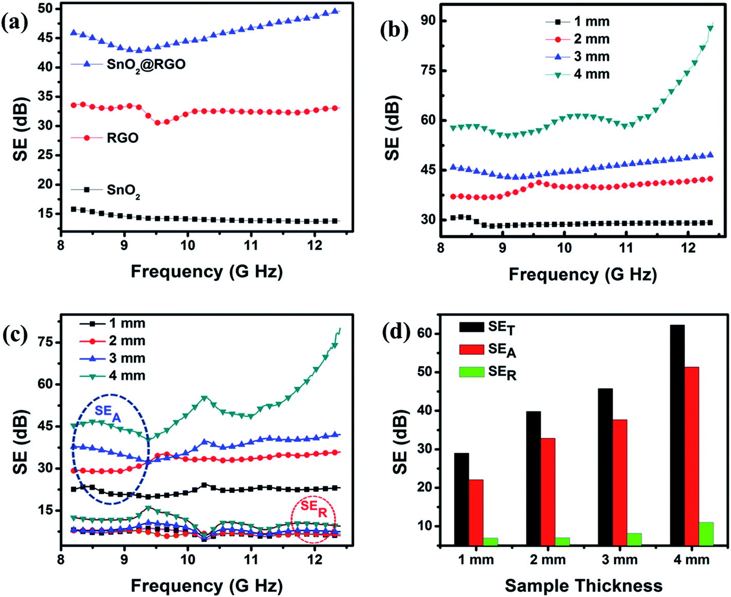 | ||
| Fig. 4 (a) Variation in EMI shielding effectiveness SET of SnO2, RGO and the SnO2@RGO composite at a critical thickness of 3 mm, (b) behavior of SET for the SnO2@RGO composite at different thicknesses (c) behavior of SEA and SER with frequency for different thicknesses of the SnO2@RGO composite and (d) SET, SEA and SER for different thicknesses of the SnO2@RGO composite. | ||
The terms SER and SEA can be defined as:25,38
|
SER = −10log(1 − R)
| (3) |
|
SEA = −10log(1− Aeff) = −10log(T/1 − R).
| (4) |
Therefore, the effective absorbance (Aeff) can be described with respect to the power of the effectively incident EM wave inside the shielding material.
| Aeff = (1 − R − T)/(1 − R) | (5) |
In terms of dielectric losses the SEA can also be written as:25
 | (6) |
In terms of tan delta the above equation can be written as:
 | (7) |
The calculated SEA and SER obtained from the experimental scattering parameters (S11, S22, S12, S21) are plotted in Fig. 4c. The values of SEA for the SnO2@RGO composite considerably increase with an increase in thickness over the entire frequency range. The SEA values of the composite with 1, 2, 3 and 4 mm thickness are in the range of 22.58–23.15, 29.19–35.90, 37.80–42.09 and 45.39–80.14, respectively. In contrast, the values of SER are very low when compared to SEA. Moreover, the change in SER is very small with an increasing thickness. Therefore, for the SnO2@RGO composite, the mechanism of shielding is mainly the absorption of EM waves due to the highly conductive composite and the absorption is proportional to the thickness of the composite material. Fig. 4d shows the overall changes in % attenuation with thickness in which changes in reflection loss with increasing thickness is very small compared to the absorption. According to the shielding theory, SEA becomes more dominant when compared to SER in the microwave range. This may be caused by the shallow skin depth and high conductivity (σac) values at such high frequencies.39,40 Although the electrical conductivity of SnO2@RGO is high (13.74 S cm−1), it is much smaller than that of graphene reported theoretically. This is because the inter transport of charge carriers in SnO2@RGO is a complex phenomenon of electron tunneling and hopping, and is different from the single layer of graphene.5,25,38,41–43 Furthermore, the conductivity of the SnO2@RGO composite is acceptable because the insulating SnO2 particles hinder the free flow of electrons in the SnO2@RGO composite.
The observed high shielding effectiveness could be explained in terms of dielectric loss. According to the EM theory, dielectric losses are the result of complex phenomena like natural resonance, dipole relaxation, electronic polarization and its relaxation, and certainly the unique structure of the shield. When the frequency of the applied field is increased, the electrons present in the system cannot reorient themselves fast enough to respond to the applied electric field and improves the dielectric constant. The SnO2 nanoparticles anchored on the top surface of the RGO sheets act as a polarized center and improves polarization, which results in more microwave shielding. High electrical conductivity of SnO2@RGO also enhances the shielding properties. SnO2 nanoparticles act as tiny dipoles, which get polarized in the presence of an EM field and result in better microwave shielding.
The curves in Fig. 4c exhibit broad multi peaks, which imply the presence of natural resonance caused by the enhanced surface anisotropy of the small size of SnO2 particles. Anisotropy energy of the small sized-materials,44 especially in the nanoscale, would be higher due to surface anisotropic field due to the small size effect.45 The higher anisotropy energy also contributes in the enhancement of the microwave shielding. Interfacial polarization occurs in heterogeneous media due to accumulation of charges at the interfaces and the formation of dipoles. Interfaces among tin oxide nanoparticles and RGO sheets further contribute to dielectric losses.
From these results, we conclude that the filling of SnO2 nanoparticles exhibit better microwave shielding properties in comparison with pristine SnO2 nanoparticles, pure RGO, γ-Fe2O3 nanoparticles, RGO–iron oxide composite, and MnO2 decorated graphene nanoribbons reported earlier.46,47
Dielectric permittivities were also investigated in order to understand the microwave shielding properties and dielectric loss mechanism of the SnO2@RGO composite in detail. Fig. 5 shows the permittivity (ε′), permittivity loss (ε′′) and tangent loss (tan δ = ε′′/ε′) as a function of frequency for the SnO2@RGO composite at a thickness of 3 mm. The permittivity symbolizes the intensity of polarization or the electrical energy storage ability of a material. The permittivity loss represents the energy loss during the activation by an EM wave. The highest value of ε′ was 160 observed at 9.6 GHz. The value of ε′′ is lower than ε′, and it fluctuates from 94 to 32 at 8.2 to 12.4 GHz. The values of the dielectric tangent loss were observed in the range of 0.85 to 0.36. The high value of ε′′ and tan δ for the SnO2@RGO composite exhibit high dielectric losses. Interestingly, there are two humps observed in the dielectric tangent loss, which proposed that the two main phenomenas are responsible for dielectric losses. These may be interfacial polarization between the SnO2 nanoparticles and RGO sheets and the effective anisotropy energy of the SnO2@RGO composite. In the effective anisotropy energy, the parallel (RGO sheets are in a plane) and random alignment of the RGO sheets were of particular importance. According to the physics principles, the polarization intensity is directly proportional to the displacement of positive and negative charges during the activation by an EM wave. When the EM waves incident perpendicular to the RGO plane, the effective anisotropy energy is higher as the polarization intensity is higher in the plane direction. Therefore, contribution to the total EMI SE is higher when the EM wave incident is perpendicular to the RGO plane than that compared to when the EM wave incident is parallel to the RGO plane.5 Furthermore, the existence of residual defects/groups in the RGO sheet48 and multiple reflections within the shield enhances the microwave shielding ability of the composites. Further, to give a visual demonstration of the microwave shielding mechanism as discussed above a schematic is given in Fig. 6. The results for the SnO2@RGO composite illustrates that such structures could be potentially used as microwave shielding materials.
 | ||
| Fig. 5 Frequency dependence of the permittivity, permittivity loss and dielectric tangent loss of the SnO2@RGO composite. | ||
 | ||
| Fig. 6 A schematic presentation of the possible microwave shielding mechanisms in the SnO2@RGO composite. | ||
4. Conclusions
In summary, we have successfully designed high performance tin oxide nanoparticles decorated RGO for suppressing electromagnetic pollution. The presence of the dielectric filler SnO2 nanoparticles on the RGO sheets enhances the dielectric losses, which can be attributed to natural resonance, dipole relaxation, electronic polarization-related relaxation, interfacial polarization and the effective anisotropy energy. Moreover, this unique SnO2@RGO composite contributes to more scattering and leads to the high shielding effectiveness (SET ∼ 62 dB at a thickness of 4 mm) when compared to conventional materials. This ingenious lightweight nanocomposite with outstanding shielding properties pushes its promising applications as a next generation building block material for EMI shielding and stealth technology.Acknowledgements
The author Monika Mishra expresses her thanks to Prof. R. C. Budhani, Director, NPL, for his keen interest in the work. The authors express their thanks to the Ministry of New and Renewable energy for sponsoring the project. The authors thank Mr Dinesh Singh for recording the TEM images of the samples. We also thank Dr R. P. Pant for XRD measurements.References
- Z.-S. Wu, G. Zhou, L.-C. Yin, W. Ren, F. Li and H.-M. Cheng, Nano Energy, 2012, 1, 107–131 CrossRef CAS PubMed.
- X. Wang, L. Zhi and K. Mullen, Nano Lett., 2007, 8, 323–327 CrossRef PubMed.
- M. Liu, X. Yin, E. Ulin-Avila, B. Geng, T. Zentgraf, L. Ju, F. Wang and X. Zhang, Nature, 2011, 474, 64–67 CrossRef CAS PubMed.
- A. P. Singh, M. Mishra, P. Sambyal, B. K. Gupta, B. P. Singh, A. Chandra and S. K. Dhawan, J. Mater. Chem. A, 2014, 2, 3581–3593 CAS.
- N. Yousefi, X. Sun, X. Lin, X. Shen, J. Jia, B. Zhang, B. Tang, M. Chan and J.-K. Kim, Adv. Mater., 2014 DOI:10.1002/adma.201305293.
- T. Xia, C. Zhang, N. A. Oyler and X. Chen, Adv. Mater., 2013, 25, 6905–6910 CrossRef CAS PubMed.
- X. C. Tong, Advanced Materials and Design for Electromagnetic Interference Shielding, Taylor & Francis, 2008 Search PubMed.
- E. A. Maguire and D. W. Readey, J. Am. Ceram. Soc., 1976, 59, 434–437 CrossRef CAS PubMed.
- W. Li, X. Qiao, H. Zhao, S. Wang and Q. Ren, J. Nanosci. Nanotechnol., 2013, 13, 793–798 CrossRef CAS PubMed.
- K. Khan, J. Supercond. Novel Magn., 2014, 27, 453–461 CrossRef CAS PubMed.
- W. Xie, H. Cheng, Z. Chu, Y. Zhou, G. Tang and Y. Xu, J. Wuhan Univ. Technol., Mater. Sci. Ed., 2007, 22, 218–220 CrossRef CAS PubMed.
- M. Matsumoto and Y. Miyata, IEEE Trans. Magn., 1997, 33, 4459–4464 CrossRef.
- V. M. Petrov and V. V. Gagulin, Inorg. Mater., 2001, 37, 93–98 CrossRef CAS.
- E. J. Borchers, C. E. Boyer, C. D. Hoyle and R. J. Kuo, Google Patents, US5085931 A, 1992.
- A. P. Singh, B. K. Gupta, M. Mishra, Govind, A. Chandra, R. B. Mathur and S. K. Dhawan, Carbon, 2013, 56, 86–96 CrossRef CAS PubMed.
- A. Saib, L. Bednarz, R. Daussin, C. Bailly, L. Xudong, J. Thomassin, C. Pagnoulle, C. Detrembleur, R. Jerome and I. Huynen, IEEE Trans. Microwave Theory Tech., 2006, 54, 2745–2754 CrossRef CAS.
- J.-M. Thomassin, X. Lou, C. Pagnoulle, A. Saib, L. Bednarz, I. Huynen, R. Jérôme and C. Detrembleur, J. Phys. Chem. C, 2007, 111, 11186–11192 CAS.
- H.-B. Zhang, Q. Yan, W.-G. Zheng, Z. He and Z.-Z. Yu, ACS Appl. Mater. Interfaces, 2011, 3, 918–924 CAS.
- X. Bai, Y. Zhai and Y. Zhang, J. Phys. Chem. C, 2011, 115, 11673–11677 CAS.
- C. Wang, X. Han, P. Xu, X. Zhang, Y. Du, S. Hu, J. Wang and X. Wang, Appl. Phys. Lett., 2011, 98, 072906 CrossRef PubMed.
- W. Choi and J. Lee, Graphene: Synthesis and Applications, Taylor & Francis, 2011 Search PubMed.
- H. Seul Ki, K. Ki Yeong, K. Taek Yong, K. Jong Hoon, P. Seong Wook, K. Joung Ho and C. Byung Jin, Nanotechnology, 2012, 23, 455704 CrossRef PubMed.
- R. Murali, Graphene Nanoelectronics: From Materials to Circuits, Springer, 2011 Search PubMed.
- M. Mishra, A. P. Singh and S. K. Dhawan, J. Alloys Compd., 2013, 557, 244–251 CrossRef CAS PubMed.
- A. P. Singh, P. Garg, F. Alam, K. Singh, R. B. Mathur, R. P. Tandon, A. Chandra and S. K. Dhawan, Carbon, 2012, 50, 3868–3875 CrossRef CAS PubMed.
- P. Sambyal, A. P. Singh, M. Verma, M. Farukh, B. P. Singh and S. K. Dhawan, RSC Adv., 2014, 4, 12614–12624 RSC.
- X.-Y. Zhang, H.-P. Li, X.-L. Cui and Y. Lin, J. Mater. Chem., 2010, 20, 2801–2806 RSC.
- Z. Xiong, L. L. Zhang, J. Ma and X. S. Zhao, Chem. Commun., 2010, 46, 6099–6101 RSC.
- S. Humaira, K. C. Kemp, C. Vimlesh and S. K. Kwang, Nanotechnology, 2012, 23, 355705 CrossRef PubMed.
- X. Zhu, Y. Zhu, S. Murali, M. D. Stoller and R. S. Ruoff, J. Power Sources, 2011, 196, 6473–6477 CrossRef CAS PubMed.
- J. Zhang, Z. Xiong and X. S. Zhao, J. Mater. Chem., 2011, 21, 3634–3640 RSC.
- S. Sladkevich, J. Gun, P. V. Prikhodchenko, V. Gutkin, A. A. Mikhaylov, V. M. Novotortsev, J. X. Zhu, D. Yang, H. H. Hng, Y. Y. Tay, Z. Tsakadze and O. Lev, Nanotechnology, 2012, 23, 485601 CrossRef CAS PubMed.
- T. K. Gupta, B. P. Singh, S. R. Dhakate, V. N. Singh and R. B. Mathur, J. Mater. Chem. A, 2013, 1, 9138–9149 CAS.
- A. C. Ferrari, J. C. Meyer, V. Scardaci, C. Casiraghi, M. Lazzeri, F. Mauri, S. Piscanec, D. Jiang, K. S. Novoselov, S. Roth and A. K. Geim, Phys. Rev. Lett., 2006, 97, 187401 CrossRef CAS.
- A. Diéguez, A. Romano-Rodríguez, A. Vilà and J. R. Morante, J. Appl. Phys., 2001, 90, 1550–1557 CrossRef PubMed.
- A. M. Nicolson and G. F. Ross, IEEE Trans. Instrum. Meas., 1970, 19, 377–382 CrossRef.
- W. B. Weir, Proc. IEEE, 1974, 62, 33–36 CrossRef.
- B. Wen, X. X. Wang, W. Q. Cao, H. L. Shi, M. M. Lu, G. Wang, H. B. Jin, W. Z. Wang, J. Yuan and M. S. Cao, Nanoscale, 2014, 6, 5754–5761 RSC.
- N. C. Das, D. Das, T. K. Khastgir and A. C. Chakrraborthy, Composites, Part A, 2000, 31, 1069–1081 CrossRef.
- N. F. Colaneri and L. W. Shacklette, IEEE Trans. Instrum. Meas., 1992, 41, 29 CrossRef.
- C. Gómez-Navarro, R. T. Weitz, A. M. Bittner, M. Scolari, A. Mews, M. Burghard and K. Kern, Nano Lett., 2007, 7, 3499–3503 CrossRef PubMed.
- S. R. Pathipati, E. Pavlica, E. Treossi, R. Rizzoli, G. P. Veronese, V. Palermo, L. Chen, D. Beljonne, J. Cai and R. Fasel, Org. Electron., 2013, 14, 1787–1792 CrossRef CAS PubMed.
- P. Lian, X. Zhu, S. Liang, Z. Li, W. Yang and H. Wang, Electrochim. Acta, 2011, 56, 4532–4539 CrossRef CAS PubMed.
- D. L. Leslie-Pelecky and R. D. Rieke, Chem. Mater., 1996, 8, 1770–1783 CrossRef CAS.
- Y.-J. Chen, P. Gao, R.-X. Wang, C.-L. Zhu, L.-J. Wang, M.-S. Cao and H.-B. Jin, J. Phys. Chem. C, 2009, 113, 10061–10064 CAS.
- K. Singh, A. Ohlan, V. H. Pham, B. R. S. Varshney, J. Jang, S. H. Hur, W. M. Choi, M. Kumar, S. K. Dhawan, B.-S. Kong and J. S. Chung, Nanoscale, 2013, 5, 2411–2420 RSC.
- T. K. Gupta, B. P. Singh, V. N. Singh, S. Teotia, A. P. Singh, I. Elizabeth, S. R. Dhakate, S. K. Dhawan and R. B. Mathur, J. Mater. Chem. A, 2013, 2, 4256–4263 Search PubMed.
- X. Sun, J. He, G. Li, J. Tang, T. Wang, Y. Guo and H. Xue, J. Mater. Chem. C, 2013, 1, 765–777 RSC.
| This journal is © The Royal Society of Chemistry 2014 |