Efficient Cu2ZnSnS4 solar cells spray coated from a hydro-alcoholic colloid synthesized by instantaneous reaction
Gerardo Larramona*,
Stéphane Bourdais,
Alain Jacob,
Christophe Choné,
Takuma Muto,
Yan Cuccaro,
Bruno Delatouche,
Camille Moisan,
Daniel Péré and
Gilles Dennler*
IMRA Europe S.A.S., 220 rue Albert Caquot, F-06904 Sophia Antipolis, France. E-mail: larramona@imra-europe.com; dennler@imra-europe.com
First published on 11th March 2014
Abstract
Efficient copper zinc tin sulphide (Cu2ZnSnS4) thin film photovoltaic devices were fabricated with a new, fast, and simple preparation method using environmentally friendly solvents. Our process is based upon a versatile and instantaneous synthesis of a Cu–Zn–Sn–S colloid. Dispersing this colloid in a mixture of water (90%) and ethanol (10%), spraying it, and annealing sequentially the samples in two different gases allowed us to grow large grain, crystalline layers of promising photovoltaic quality. We measured cell efficiencies up to 5.0% under simulated AM1.5G (cell area 0.25 cm2). To the best of our knowledge, this is the highest reported efficiency reached with Cu2ZnSnS4 using a spray deposition technique with innocuous solvents.
1 Introduction
Copper zinc tin sulphide/selenide Cu2ZnSn(S1−x,Sex)4 has recently attracted a lot of attention because of its potential to become an industrially viable thin film photovoltaic (TF-PV) material for ultra-large deployment (terawatt). This potential stems from (i) its attractive optical band-gap, (ii) its theoretical PV performances, and (iii) the large abundance and low cost of its constitutive elements. So far, the highest PV performance reported for a pure sulphide Cu2ZnSnS4 lab cell is 8.4% (0.45 cm2 area),1 while 9.2% (ref. 2) have been reached with a pure sulphide Cu2ZnSnS4 sub-module (25 cm2 total area, 14 cm2 aperture area), and between 11 and 12% (ref. 3 and 4) with Cu–Zn–Sn sulphide/selenide Cu2ZnSn(S1−x,Sex)4 devices. Several recent papers have discussed the capability of this class of materials to reach 20% efficiency.5,6 This threshold value, already attained by the parent Cu(In,Ga)Se2 (CIGS) technology,7 is commonly used as a benchmark to assess the potential viability of new TF-PV technologies on the market place. However, competitive efficiencies are not sufficient to ensure the competitiveness of a new product. Eventually, the levelised cost of energy (LCOE) dictates the sales in a subsidy free market. Therefore, it is of great importance to evaluate at an early stage of research whether a new material (in our case, Cu2ZnSnS4) can be processed with techniques compatible with mass production, ensuring high yield at high pace. This requirement implies fabrication methods which are easily up-scalable, fast and presumably low-cost (preferentially vacuum-free), as well as environmentally benign.Interestingly, the best performing Cu2ZnSn(S1−x,Sex)4 devices4 to date have been fabricated with a solution method, what could theoretically be promising in terms of production costs. However, the solvent utilized in that approach (hydrazine) is highly flammable, corrosive, toxic, and environmentally hazardous. Besides, it has both a low boiling point (115 °C), and more importantly a very low flash point (52 °C) what makes it dangerous to utilize in any industrial environments. Furthermore, among the various non-vacuum, ink-based Cu2ZnSn(S1−x,Sex)4 deposition techniques employed in the literature, the most common remains the spin-coating (either from colloidal suspensions or from precursor solutions). However, to achieve sufficiently thick and pinhole-free coatings, this method requires multiple layer applications (typically up to ten steps).8–10 Moreover, a short curing is often necessary after each spin-coating in order to avoid the dissolution of the previously deposited layers during the following spinning steps. This renders the whole process quite tedious and not easy to industrialize.
Ideally, the deposition technique utilized in the laboratory at the research stage should be easy to up-scale and transfer to a development stage. That is the case for batch and roll-to-roll compatible coating processes like spraying, ink-jetting, tape-casting, or screen printing. The latter two though demand a precise control of the viscosity of the ink, what usually requires the use of organic additives like ligands, surfactants, and thickeners. These chemicals are likely to leave carbon and other impurity traces that may jeopardize both the transport properties of the active layer and the integrity of the various interfaces comprised in the device.
Several teams working on Cu2ZnSn(S1−x,Sex)4 solar cells have employed spray deposition, especially the variety called Spray Pyrolysis Deposition (SPD).11–14 SPD involves the use of organic sulphur containing molecules like thiourea (often associated with volatile solvents) which are spray coated on the substrate. Upon annealing, the wet layer undergoes a pyrolysis which can leave a non-negligible amount of by-products. Alike in the case of printing mentioned above, these impurities can hinder the performances of the devices (to date, the best SPD coated Cu2ZnSn(S1−x,Sex)4 devices reported showed an efficiency of less than 2.4%).15 Our preferred spray approach is the non-pyrolytic one, which uses an ink made of nano-particles containing the four elements constituting the final active layer, similarly as it was made by Schulz et al.16,17 for CIGS cells. Examples of the latter for Cu2ZnSn(S1−x,Sex)4 are quite rare.18 Very recently, Zhang et al. have reported a cell efficiency of 5.4% (ref. 19) using a colloidal dispersion of Cu–Zn–Sn–S–Se in pyridine and methanol, coated with an ultrasonic spray, and annealed in an atmosphere containing H2 as well as Se and Sn vapours. The authors commented that they could not achieve good film morphologies by spraying the colloids containing only sulphur,20 and that they had to use a mixture of sulphur and selenium to achieve functional devices.
It appears clearly that pyridine and methanol used by Zhang et al. are much friendlier solvents than hydrazine. However, they remain far less versatile and benign than ethanol and water. Using the latter solvent though might induce severe hindrances as metal sulphides might get easily oxidized. Thus, the purpose of our study was to evaluate the possibility to reach reasonable cell performances by using a colloidal spray technique with an ink based exclusively on water and/or ethanol (without any organic additives). It should be noted that we have chosen to work at this stage solely with sulphur containing only Cu2ZnSn(S1−x,Sex)4, that is Cu2ZnSnS4. The main motivations for this choice are (i) the toxicity of selenium, (ii) the price and scarcity of this element, and (iii) the willingness to favour high open-circuit voltage (Voc) rather than high short-circuit photocurrent density (Jsc).
2 Experimental
All the preparations of the precursor solutions as well as the synthesis of the Cu–Zn–Sn–S colloid were carried out in a nitrogen (N2) glove box (Jacomex, France). All solvents were deoxygenated before use by bubbling N2 for 1 h. The Cu–Zn–Sn–S colloid synthesis was performed by mixing an aqueous solution of NaHS (∼0.1 M) with an acetonitrile (CH3CN) solution of the three metal chlorides, namely SnCl4, ZnCl2 and CuCl (∼1 M concentration in total metal cations). The solutions were mixed rapidly at RT and under magnetic stirring by simply pouring one solution into the other. After stirring for a few minutes, the suspension was washed in water and in ethanol (CH3CH2OH), by centrifuging the colloid, removing the supernatant and re-dispersing the precipitate in the washing solvent. The Cu–Zn–Sn atomic ratio in the metal precursors was off-stoichiometric (1.9/1.2/1 = 46–29–25%) and the NaHS solution was in 20 to 40% molar excess with respect to the metal stoichiometry.The substrates used for the Cu–Zn–Sn–S colloid deposition were commercial, 1 mm thick soda-lime glass slides covered with a Mo layer of 700 to 800 nm in thickness, deposited by sputtering (Geomatec, Japan). Before the spraying step, the Mo/glass substrates were cleaned under sonication with a soap cleaning solution (Hellmanex™, from Sigma-Aldrich), water and aqueous ammonia. Then, the Cu2ZnSnS4 films were deposited on the Mo/glass substrates by spraying an ink made of water (90 vol%)/ethanol (10 vol%) as solvents and the Cu–Zn–Sn–S colloid above mentioned. The typical Cu–Zn–Sn–S colloid concentration in the ink was 10 mg ml−1. No additives were incorporated into the ink. The home-made spray setup consisted in a commercial stainless steel nozzle, an X–Y robot, a N2 carrier gas system, a peristaltic pump for a continuous ink flow, and a hotplate. The temperature of the Mo/glass substrates during the spray was kept at about 300 °C. The nozzle moved by the robot scanned and sprayed the ink homogeneously during 10 minutes over four Mo/glass substrates of 2.5 × 2.5 cm2 each. The entire spray setup was placed inside a N2 glove box. Immediately after the spray, the films were transferred to a second N2 glove box where they were annealed on a hotplate closed with a lid (600 °C Titanium Hotplate Harry Gestigkeit, Germany). The N2 annealing profile was the following: 10 minutes ramp from RT to 200 °C, 10 minutes dwell at 200 °C, 30 minutes ramp from 200 °C to 525 °C, 15 minutes dwell at 525 °C, and finally natural cooling. An optional second annealing step was carried out in a tubular oven under a flow of 3% H2S gas diluted in argon, at 3 to 4 l h−1 at atmospheric pressure. The H2S annealing profile was the same as the N2 annealing profile, except that the dwell at 525 °C lasted 60 minutes.
The structure and the fabrication process of the photovoltaic devices were similar to the standards found in the literature, namely Ag/Indium Tin Oxide (ITO)/ZnO/CdS/Cu2ZnSnS4/Mo/soda-lime glass. The deposition of the CdS buffer layer (60 nm thick) was realized by Chemical Bath Deposition (CBD) at 60 °C during 10 min, using 80 ml of a CBD solution containing 4 mM of cadmium nitrate, 0.2 M of thiourea, and 1 M of ammonia. Prior to the CBD, the films were cleaned in water for a few minutes. In other experiments the Mo/Cu2ZnSnS4 films were chemically cleaned prior to CdS deposition by immersing them in different solutions for a few minutes. The different chemical cleaning solutions were HCl 8% (in water), 1.4 M KCN (in water–ethanol 1![[thin space (1/6-em)]](https://www.rsc.org/images/entities/char_2009.gif) :1) or 30% NH3 (in water). After such treatment, the films were thoroughly rinsed with water, and CdS deposition was carried out immediately after.
:1) or 30% NH3 (in water). After such treatment, the films were thoroughly rinsed with water, and CdS deposition was carried out immediately after.
The deposition of the undoped ZnO window layer (60 nm thick) and of the ITO layer (250 nm thick) was carried out by magnetron sputtering using a Physical Vapour Deposition (PVD) machine (Intercovamex, Mexico). No anti-reflecting coating was deposited on the top of our photovoltaic devices. Each substrate was scribed into 16 separated cells of approximately 5 × 5 mm2. A small dot of silver paste was deposited in the centre of each cell to serve as the front contact, and the Mo was contacted with indium.
Scanning Electron Microscope (SEM) images were acquired with a Field-Emission Scanning Electron Microscope Hitachi S-4700, to which an Energy-Dispersive X-ray microanalysis (EDX) Noran System SIX was coupled. EDX-SEM elemental analysis were performed using 5000× magnification, in areas of 25 × 18 μm2 (450 μm2), with a 20 kV acceleration voltage. EDX-SEM mapping analysis were done using 10000× magnification in areas of 14 × 11 μm2, 20 kV as acceleration voltage, a resolution of 64 × 48 pixels, and 100 frames with 5 s of frame time. Transmission Electron Microscopy (TEM) analysis was carried out with a JEOL 2100F FEG-200 kV microscope, having a Scanning TEM (STEM) accessory, and an integrated JEOL JED-2300T EDX analyser. Thin slices for TEM investigations were prepared by Focused Ion Beam (FIB). Additional elemental analyses were carried out by Inductively Coupled Plasma Atomic Emission Spectrometry (ICP-AES). X-Ray Diffraction (XRD) was measured with a Bruker D8 Advanced diffractometer using Cu Kα radiation and grazing incidence (typically 1°). Electric current–voltage (I–V) characteristics were recorded using a AAA-class solar simulator (Oriel Sol3A Class) used with 100 mW cm−2 irradiance. External Quantum Efficiency (EQE) was measured with an in-house setup ranging from 400 to 1100 nm wavelength, working in DC mode, with a light spot of 2 mm in diameter.
3 Results and discussion
3.1 Colloidal synthesis and characterization
The vast majority of the processes employed in the literature to form thin films of Cu2ZnSn(S1−x,Sex)4 consists in bringing the three metals (and potentially sulphur and/or selenium) in close vicinity and annealing the layer (often in sulphur and/or selenium rich vapour) to form the final crystals. In the case of the liquid particle dispersions (non-pyrolysis) approach, the most common method followed relies on the synthesis of high purity, well crystallized Cu2ZnSn(S1−x,Sex)4 nanoparticles, with typical sizes of several tens of nanometres.21–23 However, this method possesses two major drawbacks: (i) such synthesis (solvothermal or hot injection) are quite long, require high temperatures and sometimes high pressures,22,23 and (ii) they are usually based upon unfriendly chemicals like the coordinating solvent trioctylphosphine oxide (TOPO).23 An alternative approach proposed in the literature consists in preparing the nanoparticles by ball milling commercial metallic or metal sulphide powders.24 But this procedure is very long (typically 24 h by ball milling) and very costly as far as energy is concerned. Moreover, nanoparticles prepared this way usually require ligands to form a relatively stable colloid.21We believe that a colloidal dispersion of non-well crystallized nanoparticles could be an attractive precursor to obtain good films, provided that the synthesis of such colloid is simple and very rapid. This idea was initially proposed by Schulz et al. in the framework of CIGS.16,17 However, these authors did not succeed in reaching a quality of film sufficient to yield high performance devices. Nevertheless, our line of thought is encouraged by a recent study on the selenization mechanism of Cu2ZnSn(S1−x,Sex)4 films from crystalline Cu2ZnSnS4 particles:25 this report shows that the grain growth starts from the smallest (or amorphous) particles while the initially well crystallized particles are dislocated and/or decomposed, serving as material reservoir for further grain growth. Thus, our synthesis of colloidal Cu–Zn–Sn–S mixture was based on a direct precipitation at room temperature realized by mixing a solution of the three metal chlorides in acetonitrile (without any complexing agent), and a water solution of NaHS as the sulphide anion source. In order to avoid possible degradation due to oxidation and/or hydrolysis of the products, the storage and weighing of the reagents, the preparation of the solutions and the synthesis itself were all carried out inside a N2 glove box. The global stoichiometric reaction for this synthesis is the following:
| 2CuCl + ZnCl2 + SnCl4 + 4NaSH → Cu2ZnSnS4 + 4NaCl + 4HCl |
A dark brown colloid is immediately formed upon mixing the two precursor solutions. Some rinsing steps are necessary to remove the NaCl and HCl sub-products, as well as the NaHS reagent in excess. The overall yield of the synthesis (rinsing steps included) is larger than 80%. As mentioned above, we have chosen to prepare the precursors slightly off-stoichiometric: this choice was motivated by the reports of Katagiri et al.26–28 who showed that a Cu-poor and Zn-rich composition tends to yield the best photovoltaic results. Nevertheless, it is notorious that Cu2ZnSnS4 admits only a very small range of non-stoichiometry.29 Therefore some binary sulphides may have been present in our inks.
The colloid we prepared consisted of primary particles of about 10 nm in diameter, as characterized by TEM. EDX-TEM analysis indicated that the particles contained the four elements (Cu, Zn, Sn, S) finely mixed at the nanometre scale. Contrary to the colloidal synthesis reported by Zhang et al.,20 we did obtain nanoparticles with our Cu–Zn–Sn–S (sulphur only) colloid synthesis. Elemental analysis of dried colloids was carried out by ICP-AES. A Cu–Zn–Sn content of 49–29–22%, respectively, was found. This is somewhat richer in Cu and poorer in Sn than the metal precursor solution (46–29–25%). Some traces of Na (coming from the NaHS sulphide precursor) remained, the atomic content in Na being ∼1 at%, as obtained by ICP-AES. Some chlorine (Cl) traces could also be detected by EDX and ICP-AES: its exact content could not be measured accurately, but it was estimated to be lower than 0.5 at%.
3.2 Thin film characterization
As mentioned above, the Cu2ZnSnS4 thin films were deposited by spraying our colloidal ink on hot Mo/glass substrates. The as-deposited (non-annealed) Cu2ZnSnS4 films were mate dark brown. After annealing in N2 atmosphere the films became shiny grey. Fig. 1 shows some SEM images of both films. The as-deposited coatings were typically 8 to 10 μm thick and continuous, covering the whole Mo substrate without almost any pin-hole (as observed with optical microscope and SEM). The films were comprised of particles of about 10 nm in diameter, what is the same size as observed on the dried colloid. An overall porosity of roughly 50% could be estimated. Some agglomerates of the primary particles could also be distinguished: they were of different sizes and found to be already present in the ink (as observed with an optical microscope on an ink sample). After proper N2 annealing, the Cu2ZnSnS4 films were much more compact with a thickness about 3 μm, that is 2 to 3 times thinner than before annealing. The grain size increased to 1 μm with some dispersion ranging from 0.5 to 2 μm. The films were continuous and covered more than 99% of the surface of the Mo substrate: a few holes of various sizes (from pin-hole to dewettings) could be observed depending on the spray batch. Thus, as already observed by Scragg et al.30 in the case of amorphous Cu–Zn–Sn–S coated by PVD, we confirmed that even in the case of a very porous, solution processed amorphous Cu–Zn–Sn–S containing layer, a short (few minutes) annealing step under a neutral gas is sufficient to achieve compact Cu2ZnSnS4 films with large grains (micrometer-size), provided the four elements are already intimately mixed prior to the annealing. | ||
| Fig. 1 SEM images of Mo/Cu2ZnSnS4 films: as-deposited films in top (a) and cross-section (b) views, respectively; films after N2 annealing in top (c) and cross-section (d) views, respectively. | ||
We found that exposing the as-deposited films to ambient air for more than several tens of minutes hinders the formation of large grains and the compactness of the films upon annealing. We believe that such as-deposited, porous Cu2ZnSnS4 films are prone to fast surface oxidation, what can hamper the subsequent grain growth.
The composition of the Mo/Cu2ZnSnS4 films was analysed by EDX-SEM in top views. The average Cu–Zn–Sn ratio of the non-annealed films was 46–26–28% and the one of the N2-annealed films was 47–26–27%. The dispersion range was ±1.5%, what is very close to the error bar of the EDX technique itself (±1%). Thus we concluded that the N2 annealing step did not change the stoichiometry of the layer.
XRD of Cu2ZnSnS4 films are shown in Fig. 2. The XRD of as-deposited films were very similar to those of the dried colloid. They showed three very broad peaks, located at the same positions of the main peaks of Cu2ZnSnS4. The average size of the crystalline domains was found to be around 10 nm, by extracting the Full Width at Half Maximum (FWHM) of the peak at 47.44° and applying the well-known Scherrer equation. This is in agreement with the size of the primary particles detected by TEM in the dried colloid. XRD of the N2-annealed films corresponded mainly to Cu2ZnSnS4, belonging to the tetragonal space group I![[4 with combining macron]](https://www.rsc.org/images/entities/char_0034_0304.gif) . The presence of sphalerite ZnS (cubic, space group I3m) and Cu2SnS3 (ref. 31) compound (tetragonal I2m) cannot be excluded since their respective XRD peaks are coincident with the peaks of Cu2ZnSnS4. However, a few small additional peaks were clearly present, many of them corresponding to orthorhombic SnS (space group Pbnm).
. The presence of sphalerite ZnS (cubic, space group I3m) and Cu2SnS3 (ref. 31) compound (tetragonal I2m) cannot be excluded since their respective XRD peaks are coincident with the peaks of Cu2ZnSnS4. However, a few small additional peaks were clearly present, many of them corresponding to orthorhombic SnS (space group Pbnm).
 | ||
| Fig. 2 XRD at grazing incidence (1°) of Cu2ZnSnS4 films deposited on Mo/glass substrates: as-deposited (non-annealed), after N2 annealing, and after the two-step “N2 + H2S” annealing; the pattern of Cu2ZnSnS4 is added. | ||
The presence of SnS inclusions was confirmed by an elemental mapping carried by EDX-SEM (Fig. 3a). Such mapping revealed also the presence of Zn-rich and Cu-rich zones. These local inhomogeneities in composition can be explained by a partial phase segregation of Cu2ZnSnS4 into secondary phases (single or binary sulphides of Cu, Zn or Sn) upon N2 annealing. In a separate set of experiments, we investigated the effect of annealing on films deposited on bare soda-lime glass (no Mo): in that very case, XRD did not show any additional peaks besides the Cu2ZnSnS4 phase, and EDX mappings were highly homogeneous. Furthermore, Cu2ZnSnS4 films deposited on substrates made of oxide-based ceramics or glasses (SiO2 or sapphire), showed the same behaviour after N2 annealing as in the case of soda-lime glass: no appearance of secondary phases could be detected. These results allow us to conclude that, upon annealing in N2, a part of the Cu2ZnSnS4 does decompose by a reaction triggered by the Mo substrate. This decomposition may be postulated as follows, in agreement to what has been proposed previously in the literature:32,33
| 2CuI2ZnIISnIVS4 + Mo0 → MoIVS2 + 2SnIIS + 2CuI2S + 2ZnIIS |
 | ||
| Fig. 3 EDX-SEM elemental mapping of Cu–Zn–Sn elements on top views of Mo/Cu2ZnSnS4 films: (a) film after N2 annealing; (b) film after the two-step annealing “N2 + H2S”. | ||
This reaction basically suggests that the Sn(IV) in Cu2ZnSnS4 can be reduced to Sn(II) by oxidation of Mo(0) to Mo(IV).
We further investigated the mechanism of particle/grain growth and secondary phase segregation by means of a “quenching” experiment: several films were annealed under N2 following our standard heating ramp. Then, they were taken out of the hotplate at different intermediate temperatures, and quenched to room temperature. SEM images and XRD recorded on the samples quenched at 350 °C were quite similar to the ones acquired on non-annealed films. However, significant changes occurred for temperatures higher than 425 °C. From 475 °C on, all the XRD peaks of the Cu2ZnSnS4 pattern were present, indicating a good crystallization of the active layer. Simultaneously, the peaks of the secondary phases, especially SnS, appeared. Besides, at 475 °C the grains had grown over 150 nm in average, yet some film porosity still remained. Thus we believe that the formation of the secondary phases is directly linked to the particle growth and/or the film compactness. This correlates with the fact that for films deposited on bare soda-lime glass (no Mo), the Cu2ZnSnS4 grains grew only up to 500 nm for an annealing temperature of 525 °C, while some large porosity films remained, and no secondary phases could be detected.
3.3 The two-step annealing
It is notorious that the appearance of secondary phases tends to degrade the performances of the Cu2ZnSn(S1−x,Sex)4 solar cells. This is especially true for SnS and CuxS, the former having a small band gap and a shallow conduction band,34 while the latter can be metallic (for x = 1 and 1.8).35 In our case, the devices based upon the N2-annealed films showed fairly weak efficiencies of up to 2.0% only (see Section 3.4). We tried several alternative methods to anneal the as-deposited Cu2ZnSnS4 films, either by (i) changing the annealing profile in the N2 atmosphere, or by (ii) annealing the samples in various atmospheres, containing S, SnS, or SnS2 vapours (or a combination thereof) or H2S gas. As a matter of fact, none of these alternatives led to simultaneously compact and secondary phase free films: indeed, some of these annealing procedures allowed to avoid the appearance of undesired phases, but did not permit either the growth of large crystals or a reduction of the porosity of the layer.Finally, we could find an efficient annealing procedure, which allowed us to keep a good film morphology with no or very few phase segregation. This process consists in two subsequent annealing steps: a first one in pure N2, followed by a second one under H2S flow (3% in N2). We believe that the annealing in N2 allows to obtain compact films with large grains (yet triggering the formation of secondary phases), while the second annealing induces the disappearance of these secondary phases without damaging the morphology obtained after the first annealing. We propose that upon the H2S annealing, the secondary phases recombine through a redox mechanism which is the inverse of the phase segregation, and which can be postulated as follows:
| SnIIS + CuI2S + ZnIIS + H2S → Cu2ZnSnS4 + H2↑ |
We think that the H2S oxidizes the Sn(II) back to Sn(IV), thereby allowing the regeneration of the Cu2ZnSnS4 from the secondary phases. The disappearance of the secondary phases (except some excess of ZnS) was proved by XRD measurements (Fig. 2), EDX-SEM mappings (Fig. 3b), and EDX-TEM observations: Fig. 4 shows the morphological and compositional analysis of such film realized on a FIB slice extracted from a complete cell. One can see that the active layer was composed of Cu2ZnSnS4 grains and a few ZnS grains (no SnS or CuxS detected). Quantitative analyses revealed that the metal composition of the Cu2ZnSnS4 grains was almost perfectly stoichiometric (50–25–25%), within the ±1% error of the EDX-TEM technique. If one accounts for the presence of some ZnS grains, these measurements are in agreement with an overall Cu-poor Zn-rich slight off-stoichiometry. The fact that some Zn-rich zones remain in the layer is likely to be due to the non-stoichiometric (Zn-rich) starting precursor solution. This situation is clearly not perfect but largely advised both experimentally26–28 and theoretically to limit the formation of detrimental point defects (i.e. CuZn, (Cux)Sn, or SnZn).36,37 This compromise appears to be the less contra effective, as ZnS is probably the less detrimental among the different secondary phases, due to its semiconducting nature and associated large band-gap.38
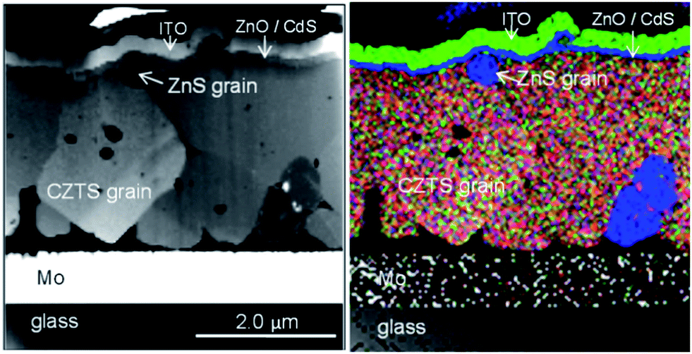 | ||
| Fig. 4 Dark-field STEM image, and corresponding EDX-TEM mapping for Cu, Zn and Sn elements in a thin slice of an ITO/ZnO/CdS/Cu2ZnSnS4/Mo cell with a Cu2ZnSnS4 film with the two-step “N2 + H2S” annealing. | ||
Finally, we would like to point out that we searched for alternatives to the usage of H2S for the second annealing step. For example, we have used vapours of sulphur as the oxidizing agent. In spite of the fact that most of the secondary phases disappeared, the morphology of the film was significantly altered. Thus the two-step “N2 + H2S” annealing process remains the best procedure we found to obtain compact films of large grains and homogenous composition.
3.4 Device performances
The respective I–V curves of the best cells fabricated with different annealing types or cleaning procedures, and recorded under simulated AM1.5G are shown in Fig. 5. As mentioned above, the films annealed only in N2 showed weak cell performances with efficiency lower than 2.0%, short-circuit photocurrent density Jsc lower that 12.0 mA cm−2, open-circuit voltage Voc lower than 0.40 V, and filling factor FF lower than 0.50. We attribute these poor properties to the presence of secondary phases, as evidenced in the sections above. On the contrary, the films annealed in two steps (N2 + H2S) yielded cells with better power output, namely an efficiency up to 3.5%, with Jsc up to 17.0 mA cm−2, Voc above 0.50 V (with a maximum at 0.60 V), and FF of 0.50. | ||
| Fig. 5 Current–voltage curves recorded under simulated AM1.5G for 3 different types of Cu2ZnSnS4 cells: film with N2 annealing (“N2”), two-step annealing (“N2 + H2S”), and two-step annealing plus HCl cleaning (“N2 + H2S + HCl”). | ||
An additional performance improvement was achieved by performing a wet chemical treatment of the Cu2ZnSnS4 film prior to the deposition of the CdS buffer layer. We tried several chemicals such as HCl, KCN or NH3 (see Experimental part). While the last two decreased the performances of the devices, the HCl cleaning led to a significant increase in efficiency, as also reported by Fairbrother et al.39 The best efficiency obtained with the films based on the two-step annealing plus HCl cleaning (sequence noted “N2 + H2S + HCl” hereafter), was 5.0%, with Jsc up to 19.0 mA cm−2, Voc up to 0.63 V, and FF of 0.50 (cell area S = 0.25 cm2).
Films with and without HCl cleaning were compared in order to explain the effect caused by this process step. SEM images did not reveal any notable differences, besides the fact that the top surface of the Cu2ZnSnS4 grains appeared more defined and sharp. This observation may indicate that a slight etching of the outmost surface took place. This latter may have removed some oxides or some secondary sulphide phases present at the top surface. TEM analyses on FIB slices indicated that (i) the ZnS grains were present in both types of films, suggesting that this HCl treatment does not eliminate ZnS impurities present in the layer and that (ii) the composition of the Cu2ZnSnS4 grains was the same within the error bar.
The dark and light (simulated AM1.5G) I–V curves of the best “N2 + H2S + HCl” cells are displayed on Fig. 6. The device parameters were obtained by fitting the I–V curve using a single diode model40 described by the following equation:
| J(V) = J0exp[q(V − RsJ)/AkT] + Gsh(V − RsJ) − JL |
 | ||
| Fig. 6 Comparison of I–V curves over a wide voltage range, at 1 sun and in dark conditions, corresponding to one of the best Cu2ZnSnS4 cells with two-step annealing plus HCl cleaning (“N2 + H2S + HCl”); serial and shunt resistances are indicated (the semi-logarithmic plot in the dark is also added). | ||
The External Quantum Efficiency (EQE) spectra recorded on various devices discussed on Fig. 5 are shown on Fig. 7.
 | ||
| Fig. 7 External Quantum Efficiency (EQE) spectra of three different types of Cu2ZnSnS4 cells: film with N2 annealing (“N2”), films annealed in two steps (“N2 + H2S”), and two-step annealing plus HCl cleaning (“N2 + H2S + HCl”). The fits to the EQE close to the bandgap (see model in text) are added as dashed lines. | ||
One can note that the maximum value reached in the “N2 + H2S + HCl” case is slightly higher than 90% at 550 nm. This suggests that the Internal Quantum Efficiency (IQE) at this wavelength is close to 100%, as the air/ITO interface reflects close to 10% of the incoming light.42 The bandgap energy (Eg) of a photoactive material can be derived from the spectral response according to the following formula:43
| ((hν) × ln(1 − EQE(hν))2 ≈ β × (hν − Eg) |
Thus, we can conclude that our devices, based upon a simple liquid process based on environmental friendly solvents shows Jsc and Voc comparable to the best ones published in the literature and measured on all vacuum processed solar cells.1 The one parameter that needs to be significantly improved is the filling factor. A modification of the spray setup and the ink conditioning could contribute to improve the morphology and reduce the numerous voids observed in the active layer and at the Mo/Cu2ZnSnS4 interface. Moreover, we probably need to reduce the amount of secondary phases which may still remain, in order to control the type and the density of the defects causing the recombination of the charge carriers. Additionally, a better tuning of the annealing procedure will certainly help as the annealing step has been found to affect enormously the properties of the Cu2ZnSnS4 film.45–47 Another parameter to be improved is the shunt resistance under illumination: its quite low value might be due to (i) pin-holes present in the Cu2ZnSnS4 layer, or (ii) a negative CBO, which might become significant in association with a recombination loss due to defects or impurities at the junction. Finally, the origin of the strong Voc deficit (0.60 eV, compared with the material band-gap of 1.5 eV) will require further investigation: for that matter, we are currently performing advanced electrical characterizations (majority carrier density, minority carrier lifetime, defects density and levels) to clarify the possible limiting factors and ways forward.
4 Conclusion
We developed a fast and simple fabrication method employing safe solvents to produce Cu2ZnSnS4 films that allowed us to achieve promising photovoltaic performances reaching 5%. This process is based upon a versatile and instantaneous synthesis of a Cu–Zn–Sn–S colloid. Dispersing this colloid in a mixture of water (90%) and ethanol (10%), spraying and sequentially annealing the layers in N2 and H2S yields compact, continuous Cu2ZnSnS4 crystalline layers with grain size of micron order. To the best of our knowledge, this achievement represents the best performances ever reached with Cu2ZnSnS4 (pure sulphide) deposited by spray. A further reduction of the remaining secondary phases and/or a better control of the formation of the number and type of defects acting as recombination centres may lead to additional improvement in our cell efficiency in a near future.Acknowledgements
The authors would like to thank Dr Simon Perraud and Dr Louis Grenet (LITEN, CEA, France) as well as Dr Thomas Unold and Dr Christian Kaufmann (Helmholtz Zentrum Berlin, Germany) for numerous inspiring discussions.Notes and references
- B. Shin, O. Gunawan, Y. Zhu, N. A. Bojarczuk, S. J. Chey and S. K. Guha, Progress in Photovoltaics: Research and Applications, 2013, 21, 72–76 CrossRef CAS.
- T. Kato, H. Homare, N. Sakai, S. Muraoka and H. Sugitomo, Proceedings 27th European Photovoltaic Solar Energy Conference and Exhibition, 2012, pp. 2236–2239 Search PubMed.
- T. K. Todorov, J. Tang, S. Bag, O. Gunawan, T. Gokmen, Y. Zhu and D. B. Mitzi, Adv. Energy Mater., 2013, 3, 34–38 CrossRef CAS.
- M. T. Winkler, W. Wang, O. Gunawan, H. J. Hovel, T. K. Todorov and D. B. Mitzi, Energy Environ. Sci., 2014, 7, 1029–1036 Search PubMed.
- D. B. Mitzi, O. Gunawan, T. K. Todorov and D. A. R. Barkhouse, Philos. Trans. R. Soc., A, 2013, 371, 1–22 CrossRef PubMed.
- S. Siebentritt, Thin Solid Films, 2013, 535, 1–4 CrossRef CAS.
- A. Chirilă, P. Reinhard, F. Pianezzi, P. Bloesch, A. R. Uhl, C. Fella, L. Kranz, D. Keller, C. Gretener, H. Hagendorfer, D. Jaeger, R. Erni, S. Nishiwaki, S. Buecheler and A. N. Tiwari, Nat. Mater., 2013, 12, 1107–1111 CrossRef PubMed.
- T. Todorov and D. B. Mitzi, Eur. J. Inorg. Chem., 2010, 17–28 CrossRef CAS.
- S. Abermann, Sol. Energy, 2013, 94, 37–70 CrossRef CAS.
- Y. E. Romanyuk, C. M. Fella, A. R. Uhl, M. Werner, A. N. Tiwari, T. Schnabel and E. Ahlswede, Sol. Energy Mater. Sol. Cells, 2013, 119, 181–189 CrossRef CAS.
- N. Nakayama and K. Ito, Appl. Surf. Sci., 1996, 92, 171–175 CrossRef CAS.
- V. G. Rajeshmon, C. S. Kartha and K. P. Vijayakumar, Solid State Phys. AIP Conference Proceedings, 2011, 1349, 683–684 CAS.
- M. Espindola-Rodriguez, M. Placidi, O. Vigil-Galán, V. Izquierdo-Rocaa, X. Fontané, A. Fairbrother, D. Sylla, E. Saucedo and A. Pérez-Rodríguez, Thin Solid Films, 2013, 535, 67–72 CrossRef CAS.
- M. Valdés, G. Santoro and M. Vázquez, J. Alloys Compd., 2014, 585, 776–782 CrossRef.
- S. Y. Kim and J. H. Kim, Thin Solid Films, 2013, 547, 178–180 CrossRef CAS.
- D. L. Schulz, C. J. Curtis, R. A. Flitton, H. Wiesner, J. Keane, R. J. Matson, P. A. Parilla, R. Noufi and D. S. Ginley, NREL/SNL Photovoltaics Program Review, 1997, 683–691 CAS.
- D. L. Schulz, C. J. Curtis, R. A. Flitton, H. Wiesner, J. Keane, R. J. Matson, K. M. Jones, P. A. Parilla, R. Noufi and D. S. Ginley, J. Electron. Mater., 1998, 27, 433–437 CrossRef CAS.
- C. Steinhagen, M. G. Panthani, V. Akhavan, B. Goodfellow, B. Koo and B. A. Korgel, J. Am. Chem. Soc., 2009, 131, 12554–12555 CrossRef CAS PubMed.
- Y. Zhang, N. Suyama, M. Goto, M. Yin and A. Yamada, Appl. Phys. Express, 2013, 6, 072302 CrossRef.
- Y. Zhang, T. Yoshihara and A. Yamada, Appl. Phys. Express, 2012, 5, 012301 CrossRef.
- Q. Guo, G. M. Ford, W. C. Yang, B. C. Walker, E. A. Stach, H. W. Hillhouse and R. Agrawal, J. Am. Chem. Soc., 2010, 132, 17384–17386 CrossRef CAS PubMed.
- O. Zaberca, F. Oftinger, J. Y. Chane-Ching, L. Datas, A. Lafond, P. Puech, A. Balocchi, D. Lagarde and X. Marie, Nanotechnology, 2012, 23, 185402 CrossRef CAS PubMed.
- K. Ramasamy, M. A. Malik and P. O'Brien, Chem. Commun., 2012, 48, 5703–5714 RSC.
- K. Woo, Y. Kim and J. Moon, Energy Environ. Sci., 2012, 5, 5340–5345 CAS.
- R. Mainz, B. C. Walker, S. S. Schmid, O. Zander, A. Weber, H. Rodriguez-Alvarez, J. Just, M. Klaus, R. Agrawal and T. Unold, Phys. Chem. Chem. Phys., 2013, 15, 18281–18289 RSC.
- H. Katagiri, K. Jimbo, M. Tahara, H. Araki and K. Oishi, Mater Res Soc Symp Proc, 2009, 1165, 125–136 CrossRef.
- H. Katagiri and K. Jimbo, Photovoltaic Specialists Conference (PVSC) 37th IEEE, 2011, 003516–003521 CrossRef.
- T. Kobayashi, K. Jimbo, K. Tsuchida, S. Shinoda, T. Oyanagi and H. Katagiri, Jpn. J. Appl. Phys., 2005, 44, 783–787 CrossRef CAS.
- I. D. Olekseyuk, I. V. Dudchak and L. V. Piskach, J. Alloys Compd., 2004, 368, 135–143 CrossRef CAS.
- J. J. Scragg, T. Ericson, X. Fontané, V. Izquierdo-Roca, A. Pérez-Rodríguez, T. Kubart, M. Edoff and C. Platzer-Björkman, Progress in Photovoltaics: Research and Applications, 2014, 22, 10–17 CrossRef CAS.
- P. A. Fernandes, P. M. P. Salomé and A. F. da Cunha, Phys. Status Solidi C, 2010, 7, 901–904 CAS.
- J. J. Scragg, J. T. Wätjen, M. Edoff, T. Ericson, T. Kubart and C. Platzer-Björkman, J. Am. Chem. Soc., 2012, 134, 19330–19333 CrossRef CAS PubMed.
- J. J. Scragg, T. Kubart, J. T. Wätjen, T. Ericson, M. K. Linnarsson and C. Platzer-Björkman, Chem. Mater., 2013, 25, 3162–3171 CrossRef CAS.
- L. A. Burton and A. Walsh, Appl. Phys. Lett., 2013, 102, 132111 CrossRef.
- G. Dennler, R. Chmielowski, S. Jacob, F. Capet, P. Roussel, S. Zastrow, K. Nielsch, I. Opahle and G. K. H. Madsen, Adv. Energy Mater DOI:10.1002/aenm.201301581.
- D. Han, Y. Y. Sun, J. Bang, Y. Y. Zhang, H. B. Sun, X. B. Li and S. B. Zhang, Phys. Rev. B: Condens. Matter Mater. Phys., 2013, 87, 155206 CrossRef.
- S. Chen, A. Walsh, X. G. Gong and S. H. Wei, Adv. Mater., 2013, 25, 1522–1539 CrossRef CAS PubMed.
- J. Just, D. Lützenkirchen-Hecht, R. Frahm, S. Schorr and T. Unold, Appl. Phys. Lett., 2011, 99, 262105 CrossRef.
- A. Fairbrother, E. García-Hemme, V. Izquierdo-Roca, X. Fontané, F. A. Pulgarín-Agudelo, O. Vigil-Galán, A. Pérez-Rodríguez and E. Saucedo, J. Am. Chem. Soc., 2012, 134, 8018–8021 CrossRef CAS PubMed.
- S. S. Hegedus and W. N. Shafarman, Progress in Photovoltaics: Research and Applications, 2004, 12, 155–176 CrossRef CAS.
- M. Bär, B. A. Schubert, B. Marsen, R. G. Wilks, S. Pookpanratana, M. Blum, S. Krause, T. Unold, W. Yang, L. Weinhardt, C. Heske and H. W. Schock, Appl. Phys. Lett., 2011, 99, 222105 CrossRef.
- H. Wu, L. Hu, T. Carney, Z. Ruan, D. Kong, Z. Yu, Y. Yao, J. J. Cha, J. Zhu, S. Fan and Y. Cui, J. Am. Chem. Soc., 2011, 133, 27–29 CrossRef CAS PubMed.
- G. Zoppi, Progress in Photovoltaics: Research and Applications, 2009, 17, 315–319 CrossRef CAS.
- J. Pankove, Optical Processes in Semiconductors, Dove Publication, New York, 1971 Search PubMed.
- H. Katagiri, K. Jimbo, W. S. Maw, K. Oishi, M. Yamazaki, H. Araki and A. Takeuchi, Thin Solid Films, 2009, 517, 2455–2460 CrossRef CAS.
- A. Emrani, P. Vasekar and C. R. Westgate, Sol. Energy, 2013, 98, 335–340 CrossRef CAS.
- L. Choubrac, M. Paris, A. Lafond, C. Guillot-Deudon, X. Rocquefelte and S. Jobic, Phys. Chem. Chem. Phys., 2013, 15, 10722–10725 RSC.
| This journal is © The Royal Society of Chemistry 2014 |