Continuous synthesis of colloidal chalcopyrite copper indium diselenide nanocrystal inks

Ki-Joong Kim, Richard P. Oleksak, Changqing Pan, Michael W. Knapp, Peter B. Kreider, Gregory S. Herman and Chih-Hung Chang*
School of Chemical, Biological & Environmental Engineering, Oregon State University, Corvallis, OR 97331, USA. E-mail: Chih-hung.chang@oregonstate.edu

Received 23rd February 2014 , Accepted 21st March 2014

First published on 25th March 2014


Abstract

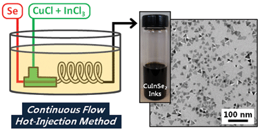
A continuous synthetic method in a micro-tubular reactor is introduced for synthesizing mono-disperse and solution-stable chalcopyrite colloidal copper indium diselenide nanocrystal (CuInSe2 NC) inks with potential scalability. It was found that the morphologies of the CuInSe2 NCs were dependent on the Cu/In/Se composition. The NC morphology changed from spherical to hexagonal to trigonal with increasing In or Se content, whereas trigonal morphologies synthesized at high temperature yielded chalcopyrite CuInSe2 NCs. A laboratory-scale photovoltaic device with 1.9% efficiency under AM1.5G illumination was also fabricated to verify the utility of these inks.


Introduction

The ternary I–III–VI2 chalcopyrite semiconductor has been intensely studied for photovoltaic (PV) applications due to the suitability of the band gap and high absorption coefficient1–3 and more recently as a nontoxic alternative to cadmium-based quantum dots (QD).4–6 Copper indium diselenide (CuInSe2) is considered a good candidate for PV applications since it has a band gap of ∼1.0 eV, a high absorption coefficient, good radiation stability, low toxicity, and high PV efficiency.7,8 Various deposition techniques have been used to make solar cells based on CuInSe2. The high cost and the scale-up difficulties associated with vacuum based synthesis have led many to investigate solution based routes to solar cell fabrication.9–16 Among these, colloidal synthesis of nanocrystals (NC) which may be dispersed to form solutions of stable inks has recently gained much attention due to the long term stability when compared to other solution based precursors.17 This allows for large area deposition of the absorber layer in a single step using existing printing technologies.18

The ability to produce stable, high-quality NC inks in solution with high-throughput is a key step in the development of low-cost thin film and QD-based solar cells19 and light emitting diodes.17,20–22 The ability to control the uniformity of the size, shape, composition, crystal structure and surface properties of the NCs is also of technological interest.23–25 Several methods have been reported in the literature for the synthesis of CuInSe2 NCs, however synthesis of high quality NCs has typically been limited to small batch reactors (∼25 mL) leading to low production rates.12 Furthermore, vessel temperature and mass transfer characteristics are not well defined for these small batch reactors and significant variation in product results is commonly observed, especially if the batch size is increased. These problems make it difficult to scale up of CuInSe2 NC production based on synthetic processes developed for small batch reactors, and may limit the commercial scale fabrication of solar cells.

Several techniques have been reported for the synthesis of CuInSe2 NCs. Among these, the most common utilize organic solvents either in a high pressure environment, i.e. the solvothermal method26 or via small scale inert environment Schlenk line experiments where precursors are either mixed at room temperature followed by slow heating,27 or hot-injected28 to give burst nucleation. In particular, the hot-injection method has been widely used to produce mono-dispersed CuInSe2 NCs with good control over NC size. The most thoroughly studied hot-injection route utilizes oleylamine (OLA) as the sole reaction medium acting as both solvent and ligand.9,12,29 In a typical hot-injection method a room temperature Se precursor solution is injected into CuCl and InCl3 precursor solutions held at high temperature leading to the kinetically determined formation of CuInSe2 NCs of disordered sphalerite phase.9,29 These investigations have shown that reaction condition is a critical factor in the crystal phase determination.

Recently, we have reported a scalable, continuous flow microreactor for the synthesis CuInSe2 NCs.30 This method combines the high synthesis quality with the potential scalability and reduced batch-to-batch variation of a continuous flow process. Herein we introduce a continuous synthetic method in a micro-tubular for generating mono-disperse and solution-stable chalcopyrite CuInSe2 colloidal NC inks and demonstrate their use in PV application. Furthermore, we elucidate a relationship between the composition and morphology of the CuInSe2 NCs and propose a morphology based reaction pathway.

Experimental

Chemicals

Copper chloride (CuCl, >90%), indium chloride (InCl3, 99.99%), and selenium powder (Se, 99.5%) were purchased from Alfa Aesar. Technical grade oleylamine (OLA, >70%) and anhydrous toluene (>99.5%) were obtained from Sigma-Aldrich and ACS grade of ethanol (>99.5%) from Macron chemicals. All chemicals were used as purchased without further purification.

Synthesis of CuInSe2 nanocrystals (NCs)

CuInSe2 NCs were synthesized by a continuous flow system as shown in Fig. 1. Two media storage bottles (100 mL, KIMAX) with two holes were placed on a hot plate; one hole was connected to a vacuum purge line and a thermocouple was inserted through the other hole for temperature monitoring. A mixture of CuCl (0.66 mmol), InCl3 (0.66 mmol), and OLA (60 mL) was stirred in the first bottle under vacuum at 80 °C for 60 min and then purged with Ar gas (99.9999%) at 130 °C for 60 min. This solution was marked solution A. Meanwhile, Se (1.32 mmol) was added to 20 mL of OLA in a second bottle and stirred under vacuum at 80 °C for 60 min and then purged with Ar gas (99.9999%) at 130 °C for 180 min. This solution was marked solution B.
image file: c4ra01582g-f1.tif
Fig. 1 Schematic diagram of (A) continuous synthetic system and (B) detailed tee in an oil bath indicated by red-colored in (A).

In a typical synthesis, each solution was continuously pumped using a peristaltic pump (REGLO Digital, Ismatec) into Tygon tubing (1.52 mm i.d., Upchurch Scientific) at a flow rate of 0.3 mL min−1 and 0.1 mL min−1 for solutions A and B, respectively. Both precursors were connected with Ar gas in a Tedlar bag while pumping in order to keep an inert environment. Solution A initially flowed into a stainless steel tee immersed in an oil bath maintained at the desired reaction temperature. Solution B was injected using a stainless steel gauge needle (o.d.: 0.91 mm, i.d.: 0.6 mm) which was inserted into a stainless steel tee with the needle tip located at the exit of the tee. As shown in Fig. 1, both precursor solutions were heated to reaction temperature in the oil bath prior to mixing. The reaction was carried out in a 4 m long PTFE tubing (o.d.: 3.18 mm, i.d.: 1.59 mm, wall: 0.79 mm) corresponding to a residence time of 20 min. The reaction product was collected in a 30 mL glass vial for 10 min, and then 10 mL of ethanol was added to precipitate the NCs, followed by centrifugation at 7000 rpm for 10 min. The supernatant was discarded and 10 mL of toluene and 5 mL of ethanol were added to the NCs followed by an additional 7000 rpm for 10 min. The supernatant was decanted, and the final product was re-dispersed in 5 mL of toluene or dried under vacuum for further characterization. Typically, CuInSe2 NC powder was obtained at a rate of ∼42 mg h−1.

CuInSe2 thin film PV fabrication

CuInSe2 nanocrystals (NCs) based PV device was fabricated with the structure of glass/Mo/CuInSe2/CdS/i-ZnO/n-ZnO:Al. Before coating, the CuInSe2 NCs were washed with iso-propanol 5 times and then re-dispersed in 5 mL toluene and 20 μL OLA. The CuInSe2 film was coated by drop casting the concentrated NCs on Mo-coated glass substrate twice. After each layer coating, the film was dried at 150 °C under vacuum for 20 minutes. Next, the film was annealed in a quartz tube furnace with 5%-H2 flowed at 500 °C for 30 minutes. 0.3 g Se powder was loaded in a crucible to prevent significant loss of Se from the film. After selenization, CdS buffer layer was coated by chemical bath deposition on the sample. Then, ∼50 nm i-ZnO and 250 nm Al doped n-ZnO window layers were deposited by RF magnetron sputtering on top of CdS layer. 500 nm Al top-contacts were deposited as a current collector using a thermal evaporator. The finished devices were mechanically scribed into 3 mm by 3 mm small cells for efficiency study.

Characterization

The crystalline phases were identified by X-ray diffraction (XRD) (D8 Discover, Bruker) operating at 40 kV and a current of 40 mA with Cu Kα1 radiation (0.154 nm) in the 2θ scan range from 20° to 90° with a step size of 0.05°. The ultraviolet-visible absorption (UV-Vis) spectrum was measured using a UV-Vis-NIR spectrophotometer (V-670, Jasco) in the range of 300–1500 nm. The absorption spectra were recorded using 10 mm path length quartz cuvettes. The size and morphology of the samples were observed using a high resolution transmission electron microscopy (HRTEM) (Titan 80-300, FEI) as well as atomic-resolution high-angle annular dark-field scanning transmission electron microscope (HAADF-STEM) operating at 300 kV in conjunction with energy dispersive spectroscopy (EDS). The solution containing NCs was dropped onto a carbon-coated gold grid (300 mesh, Ted Pella Inc.). Average particle sizes were determined by manually counting at least 450 particles in the micrographs. The electron diffraction patterns were obtained by Fourier transform patterns of the HRTEM images. EDS spectra of bulk NCs were obtained using an FEI Quanta 600 FEG SEM operating at 30 kV on samples prepared by drop-casting a thick film of NCs onto a Si substrate and dried under N2 gas flow. Spectra were collected for four random locations on the sample with the average values reported. EDS spectra of individual NCs were obtained in the TEM described above operating in HAADF-STEM mode by resting the electron beam probe (point resolution 0.14 nm) on the particle being analysed. Spectra were collected for three particles of each shape with the average values reported. For all EDS measurements the error indicated represents the estimated standard error (i.e. σ/√n). PV device performance was measured using an Oriel 96000 Full spectrum solar simulator calibrated with a standard Si solar cell and Newport radiant power meter and PVIV-200 test station.

Result and discussion

The crystal structure of the CuInSe2 NCs synthesized at different reaction temperatures (200 °C, 220 °C and 240 °C) for 20 min via the continuous synthetic method were investigated using XRD (Fig. 2A). The XRD pattern for the 200 °C reaction could be indexed exclusively to tetragonal phase Cu3Se2 (JCPDS no. 47-1745). For the 220 °C reaction Cu3Se2 peaks disappear and new peaks are observed at 27.0°, 44.9°, and 53.1° which can be indexed to the (111), (220) and (311) planes of cubic phase Cu2−xSe (JCPDS no. 06-0680), respectively, along with peaks corresponding to CuInSe2 (JCPDS no. 40-1487). For the 240 °C reaction the XRD pattern can be indexed exclusively to the chalcopyrite (tetragonal) phase of CuInSe2 (JCPDS no. 40-1487) with an intense peak at 2θ = 26.6° corresponding to the (112) diffraction plane. The other distinct peaks with 2θ values of 44.2°, 52.4°, and 70.8° could be indexed to (204)/(220), (312)/(116) and (316)/(332) planes of tetragonal CuInSe2. In addition to these intense peaks, weaker peaks were observed at 27.8°, 30.9°, 35.5°, and 64.3° which correspond to the (103), (200), (211), (400) planes, and are unique to the chalcopyrite CuInSe2 phase.
image file: c4ra01582g-f2.tif
Fig. 2 (A) XRD patterns and (B) UV-Vis absorption spectra (inset shows the optical energy gap of CuInSe2 NCs synthesized at 240 °C) of NCs synthesized at different reaction temperatures for 20 min by continuous synthetic method. The absorption indicated by the asterisk is the band from the solvent.

The XRD results indicate that the lower temperature reaction products were comprised primarily of copper selenide intermediates (i.e. Cu3Se2 and Cu2−xSe). No indium selenide intermediates were observed for these reaction conditions, suggesting the NC formation follows a similar pathway to that which was reported previously for the synthesis of CuInSe2 using an OLA solvent.29 That is, the thermodynamically favorable chalcopyrite CuInSe2 phase is generated primarily through the solid–liquid reaction of copper selenides and dissolved InCl3 for extended reaction times. It has also been shown that synthetic routes using OLA leads to CuInSe2 NCs with disordered sphalerite structure in the case of hot-injection method, whereas the chalcopyrite phase is formed in the case of slow heating of all dissolved precursors in one pot.28 In our study, both Cu/In and Se precursor solutions are maintained above the nucleation temperature prior to mixing. This allows for the thermodynamically controlled formation of the stable chalcopyrite phase. In a prior study of continuous synthetic method of CuInSe2 NCs using a solvent system of oleic acid (OA) and tri-n-octylphosphine (TOP), it has shown that both copper selenide and indium selenide binary intermediates were formed and that the rate limiting step for synthesis of CuInSe2 was formation of indium selenide.30 In the current study, we observed no evidence of indium selenide formation in the final products. This is not surprising due to the significantly different solvent systems used which will undoubtedly play a role in NC formation. In particular, herein Se dissolved in OLA is immediately available for NC nucleation upon mixing of the precursors, whereas in the prior study30 decomposition of TOP[double bond, length as m-dash]Se molecules precedes nucleation. Furthermore, it is expected that the different bonding strengths of OLA to dissolved precursors and nucleated NCs in comparison to OA and TOP will affect the reaction pathway and thus the synthesis herein is more likely to follow that reported for a previous detailed spectroscopic study of CuInSe2 formation in OLA29 as discussed above.

As indicated by XRD, the Cu2−xSe phase is converted to the chalcopyrite CuInSe2 phase at higher temperatures which provide sufficient activation energy for phase conversion. These findings are consistent with those of previous reports in literature that indicate the Cu ions diffuse out of the Cu2−xSe phase into the solvent with increasing temperature, allowing for the inclusion of In ions into the structure of Cu2−xSe, which leads to the formation of chalcopyrite CuInSe2 phase.31

The absorption spectra of the CuInSe2 NCs synthesized at different reaction temperatures were measured using UV-Vis absorbance spectroscopy (Fig. 2B). A broad and intense absorbance peak for the NCs synthesized at 200 °C was observed at 1050 nm, which is attributed to transitions involving the indirect band gap of copper selenide.32,33 These absorbance peaks gradually decreases with an increase in reaction temperature due to the decrease in copper selenide intermediates, which is in agreement with the XRD data. The composition in the ternary I–III–VI2 compounds can significantly influence their band gap properties.34 For each reaction condition, the band gap was determined by extrapolating the linear region of a plot of the squared absorbance versus the photon energy (Fig. 2B inset). Band gap values are seen to vary in the range of 2.45–1.10 eV as the reaction temperature increases from 200 °C to 240 °C. Although the band gap of copper selenide is not well defined because of the wide variety of stoichiometric ratios, bulk copper selenide such as Cu3Se2 and Cu2−xSe are typically reported to possess a direct band gap of 2.1–2.4 eV and an indirect band gap of 1.2–1.7 eV.33 The obtained band gap values are consistent with a decrease in copper selenide with increasing reaction temperature. The band gap of the CuInSe2 NCs synthesized at 240 °C was found to be 1.10 eV, which is in a good agreement with that of bulk chalcopyrite CuInSe2 (1.04 eV).35

The morphologies of NCs synthesized at different reaction temperatures were observed by TEM and are found to change with increasing reaction temperature (Fig. 3). It can also be seen that the NCs are uniform in size with a mixture of spherical, hexagonal, and trigonal shapes. At 200 °C, a large fraction of spherical/hexagonal NCs were observed with an average size of 14.7 nm (Fig. 3A). Similar morphologies are observed for the 220 °C reaction temperature (Fig. 3B) with a slight increases average size of 15.6 nm. Very uniform trigonal NCs were observed at 240 °C reaction temperature with an average size of 16.2 nm and a 1.8 nm standard deviation indicating a fairly narrow size distribution (Fig. 3C). All these samples exhibit good monodispersity as indicated by the histograms of their size distributions as shown in Fig. 3E–G.


image file: c4ra01582g-f3.tif
Fig. 3 (A–C) TEM images and (D) an example of EDS spectrum of mono-disperse NCs synthesized at different reaction temperatures for 20 min by continuous synthetic method (see more details in the Table 1). The average particle sizes of the NCs synthesized at 200 °C, 220 °C and 240 °C were 14.7 ± 2.9 nm, 15.6 ± 3.1 nm and 16.2 ± 1.8 nm, respectively. (E–G) Histograms of the NCs synthesized at different reaction temperatures ((E): 200 °C, (F): 220 °C and (G): 240 °C).

A prior study has reported the synthesis of CuInSe2 NCs with trigonal shape using a batch reactor with a selenourea (SeC(NH2)2) Se precursor and OLA solvent.36 The existence of trigonal shapes is thus likely related to the preferred growth of CuInSe2 NCs along certain crystal facets in the OLA solvent system. The presence of exclusively trigonal shapes for the 240 °C reaction therefore suggests the reaction has gone to completion and consists exclusively of CuInSe2, in agreement with XRD and EDS measurements. The Cu/In/Se compositions of the NCs synthesized at different reaction temperatures were analyzed by EDS (Fig. 3D), which showed varying ratios of Cu[thin space (1/6-em)]:[thin space (1/6-em)]In[thin space (1/6-em)]:[thin space (1/6-em)]Se compositions at different reaction temperatures. The compositions of Cu/In/Se tend to approach the desired stoichiometry of 1[thin space (1/6-em)]:[thin space (1/6-em)]1[thin space (1/6-em)]:[thin space (1/6-em)]2 when reaction temperature increases to 240 °C, with a slight excess of Se (Table 1).

Table 1 EDS elemental analysis of bulk CuInSe2 NCs synthesized at different temperatures
Reaction temperature (°C) Compositions (atomic%) Atomic ratios
Cu In Se
200 41.4 ± 0.4 9.6 ± 0.4 49.0 ± 0.1 (1.00[thin space (1/6-em)]:[thin space (1/6-em)]0.23[thin space (1/6-em)]:[thin space (1/6-em)]1.18)
220 31.3 ± 1.0 18.6 ± 0.5 51.3 ± 0.6 (1.00[thin space (1/6-em)]:[thin space (1/6-em)]0.60[thin space (1/6-em)]:[thin space (1/6-em)]1.64)
240 23.6 ± 0.1 23.3 ± 0.1 53.1 ± 0.2 (1.00[thin space (1/6-em)]:[thin space (1/6-em)]0.99[thin space (1/6-em)]:[thin space (1/6-em)]2.25)


HAADF-STEM EDS analysis was conducted to ascertain the Cu/In/Se compositions for individual NCs of different shape (Fig. 4). The 220 °C reaction product was used since this contained all three types of the observed morphologies (spherical, hexagonal, and trigonal). EDS results reveal the absence of In ions for spherical NCs which showed a Cu/In/Se = 1.00 ± 0.02[thin space (1/6-em)]:[thin space (1/6-em)]0.00[thin space (1/6-em)]:[thin space (1/6-em)]0.78 ± 0.01 which is attributed to the Cu3Se2 or Cu2−xSe phase; while the hexagonal NCs consists of Cu, In, and Se with an atomic ratio of 1.00 ± 0.03[thin space (1/6-em)]:[thin space (1/6-em)]0.22 ± 0.15[thin space (1/6-em)]:[thin space (1/6-em)]1.16 ± 0.04. Based on the XRD data, initially Cu3Se2 is formed, followed by the formation of Cu2−xSe, and finally the gradual incorporation of In ions into the structure of the Cu2−xSe NCs, where an increase in the reaction temperature leads to an increase in In ions content. This led to an insufficient In ions content for CuInSe2 NCs synthesized at the low temperature. The composition of trigonal shaped NCs showed a Cu/In/Se = 1.00 ± 0.07[thin space (1/6-em)]:[thin space (1/6-em)]1.03 ± 0.09[thin space (1/6-em)]:[thin space (1/6-em)]1.99 ± 0.01 suggesting they are CuInSe2. These results also suggest the shape of synthesized NCs may be correlated to their Cu/In/Se compositions.


image file: c4ra01582g-f4.tif
Fig. 4 (A) HADDF-STEM image and (B) an example of EDS spectrum collected for individual NCs synthesized at 220 °C. The labeled NCs in (A) and corresponding EDS spectra in (B) are representative of NCs chosen for analysis of each morphology i.e. spherical (S), hexagonal (H) and trigonal (T). The Au peaks in EDS spectra come from the carbon coated gold grid.

To gain more insight into the crystal structure for individual NCs, HRTEM (Fig. 5A–C) and Fourier transform (FT) (Fig. 5D–F) analysis were used. The two fold symmetric spots in FT images indicate that all the individual NCs are single crystalline in structure. Fig. 5A shows the HRTEM image of the spherical NC. The resolved interplanar spacing is 0.322 nm, corresponding to the (200) lattice plane (Fig. 5D) of tetragonal phase Cu3Se2 (JCPDS no. 47-1745). The lattice spacing of hexagonal NC (Fig. 5B) with an insufficient In content are 0.333, 0.288, and 0.203 nm, respectively. The lattice plane of the hexagonal NC is also given by the FT pattern (Fig. 5E). Longer distances of d-spacing indicate that the inclusion of In ions causes distortion of the copper selenides structure.


image file: c4ra01582g-f5.tif
Fig. 5 HRTEM images for individual NCs with different composition of Cu/In/Se atomic ratios ((A): spherical, (B): hexagonal, (C): trigonal) and their FT images ((D): spherical, (E): hexagonal, (F): trigonal) of CuInSe2 NCs synthesized at different reaction temperatures. (G) Schematic illustration of the morphological transformation for CuInSe2 NCs synthesized by continuous flow hot-injection method.

The spacing of the lattice planes of the trigonal NC in the HRTEM images (Fig. 5C) shows predominant spots in the FT image (Fig. 5F). These spots could be indexed to the tetragonal phase of CuInSe2 with a = b = 0.5782 nm and c = 1.1619 nm lattice parameters using the CaRine Crystallography software. This is evidence that the morphology change to the trigonal NCs is accompanied by the phase conversion to chalcopyrite structure.

Several groups have reported the synthesis of mono-disperse and solution-stable CuInSe2 NCs using batch reactors,9,12–14,36 however the relationship between morphology and composition has not yet been reported. Here we propose the evolution of CuInSe2 NCs from spherical/hexagonal and finally trigonal shapes as the reaction temperature is increased and the reaction proceeds to completion. A schematic diagram of the process is presented in Fig. 5G. Morphologies of the CuInSe2 NCs are observed to be dependent on Cu/In/Se ratio. As reaction temperature is increased, the spherical NCs are transformed to hexagonal NCs which gradually incorporate In and/or Se ions, finally resulting in trigonal shaped CuInSe2 NCs.

Laboratory-scale PV device was also fabricated to verify the utility of these inks. Chalcopyrite CuInSe2 NCs synthesized herein were used to fabricate a PV device via drop casting on Mo-coated glass and was subjected to annealing at 500 °C in a selenium environment. The final stack consisted of glass/Mo/CuInSe2/CdS/i-ZnO/n-ZnO:Al. XRD patterns of the CuInSe2 NCs synthesized at 240 °C and CuInSe2 thin film after selenization on Mo/glass substrate shows only sharpening of existing chalcopyrite CuInSe2 peaks indicating the annealed CuInSe2 thin film exhibited significant grain growth while remaining phase pure (Fig. 6). The diffraction peaks from Mo and MoSe2 are detectable from the substrate and interfacial layers directly under the CuInSe2 thin film. Peaks arising from the Mo substrate and the MoSe2 interlayer are indicated.


image file: c4ra01582g-f6.tif
Fig. 6 XRD patterns of (A) CuInSe2 NCs synthesized at 240 °C by continuous flow hot-injection method and (B) CuInSe2 thin film on Mo/glass substrate after selenization at 500 °C for 30 minutes.

Fig. 7 shows the current–voltage (IV) characteristics of the PV device and an FE-SEM image of the cell cross section is included as Fig. 7 inset. As seen in the cross section the CuInSe2 NC film experienced significant crystallization with grains as large as 1–2 μm. The device exhibited a power conversion efficiency of 1.9% under AM1.5 illumination (open circuit voltage = 347 mV, short circuit current density = 19.8 mA cm−2, fill factor = 28%). This efficiency is comparable to previously reported CuInSe2 thin film solar cells using single phase CuInSe2 NCs as precursors ink.7,9,12,37–39 One of the primary efficiency limitations of this device is the low fill factor suggesting a high series resistance which is likely related to the large film thickness of 4.5 μm, which is 3–4 times the thickness typically required to absorb all incident photons. Higher efficiency cells have also been reported using multiphase NC phase ink.39 Further optimization of the PV device fabrication and modification of the precursor components should lead to significant increases in efficiency using these inks.


image file: c4ra01582g-f7.tif
Fig. 7 (A) Photograph of CuInSe2 NCs thin film deposited on Mo coated glass by drop casting of the CuInSe2 NCs ink after selenization. (B) Photograph of completed photovoltaic device. (C) The current–voltage (IV) characteristic of the fabricated PV device under AM1.5 illumination. Inset shows a representative cross section field-emission scanning electron microscope image of a completed CuInSe2-based PV device after chemical bath deposition of CdS, sputtering of i-ZnO and n-ZnO:Al, and evaporation of metal contacts. VOC, JSC, FF, and PCE denote open circuit voltage, short circuit current density, fill factor, and power conversion efficiency, respectively.

Conclusions

In summary, a continuous synthetic route for synthesizing mono-disperse and solution stable trigonal CuInSe2 NC “inks” has been introduced in which common reactants CuCl, InCl3, and Se are used and OLA is used as a both solvent and capping agent. The morphology of the CuInSe2 NCs synthesized by continuous synthetic method is found to be related to the Cu/In/Se compositions. These results provide the possibility to estimate the Cu/In/Se compositions in CuInSe2 NCs based on the observed morphology of the particles. It is also found that copper selenide intermediates react with In ions at higher reaction temperatures. Here, the lattice distortion of copper selenide occurred by inclusion of In ions leading to phase conversion into a chalcopyrite CuInSe2 structure. This continuous synthetic method could significantly reduce the cost of CuInSe2 and other I–III–VI (CuInS2, CuInGaSe2, Cu2ZnSn(S,Se)4, etc.) colloidal NCs production. As a proof of concept a CuInSe2-based PV device was fabricated with a PCE of 1.9% and it is expected that further optimization of the PV device fabrication should lead to significant increases in PV efficiency.

Acknowledgements

The authors gratefully acknowledge funding from the Oregon Nanoscience and Microtechnologies Institute GAP program. A portion of this work was performed at the Oregon Process Innovation Center for Sustainable Solar Cell Manufacturing, an Oregon BEST signature research facility. PBK was supported by the National Science Foundation's Process and Reaction Engineering program under an EAGER grant no. CBET-1105061. We are thankful to Joshua Raznik at CAMCOR, University of Oregon, for his valuable assistance in obtaining, analyzing and interpreting HRTEM data.

Notes and references

  1. B. J. Stanbery, Crit. Rev. Solid State Mater. Sci., 2002, 27, 73 CrossRef CAS.
  2. M. Kemell, M. Ritala and M. Leskela, Crit. Rev. Solid State Mater. Sci., 2005, 30, 1 CrossRef CAS.
  3. S. Siebentritt, Sol. Energy Mater. Sol. Cells, 2011, 95, 1471 CrossRef CAS PubMed.
  4. D. Aldakov, A. Lefrancois and P. Reiss, J. Mater. Chem. C, 2013, 1, 3756 RSC.
  5. O. Chen, H. Wei, A. Maurice, M. Bawendi and P. Reiss, MRS Bull., 2013, 38, 696 CrossRef CAS.
  6. E. Cassette, T. Pons, C. Bouet, M. Helle, L. Bezdetnaya, F. Marchal and B. Dubertret, Chem. Mater., 2010, 22, 6117 CrossRef CAS.
  7. V. A. Akhavan, B. W. Goodfellow, M. G. Panthani, D. K. Reid, D. J. Hellebusch, T. Adachi and B. A. Korgel, Energy Environ. Sci., 2010, 3, 1600 CAS.
  8. W.-J. Wang, Y. Jiang, X.-Z. Lan, C. Wang, X.-M. Liu, B.-B. Wang, J.-W. Li, B. Yang and X.-N. Ding, Mater. Sci. Semicond. Process., 2012, 15, 467 CrossRef CAS PubMed.
  9. Q. Guo, S. J. Kim, M. Kar, W. N. Shafarman, R. W. Birkmire, E. A. Stach, R. Agrawal and H. W. Hillhouse, Nano Lett., 2008, 8, 2982 CrossRef CAS PubMed.
  10. D. B. Mitzi, Adv. Mater., 2009, 21, 3141 CrossRef CAS PubMed.
  11. M. E. Norako and R. L. Brutchey, Chem. Mater., 2010, 22, 1613 CrossRef CAS.
  12. M. G. Panthani, V. Akhavan, B. Goodfellow, J. P. Schmidtke, L. Dunn, A. Dodabalapur, P. F. Barbara and B. A. Korgel, J. Am. Chem. Soc., 2008, 130, 16770 CrossRef CAS PubMed.
  13. H. Zhong, Y. Li, M. Ye, Z. Zhu, Y. Zhou, C. Yang and Y. Li, Nanotechnology, 2007, 18, 025602 CrossRef.
  14. J. Tang, S. Hinds, S. O. Kelly and E. H. Sargent, Chem. Mater., 2008, 20, 6906 CrossRef CAS.
  15. W. Wang, Y.-W. Su and C.-H. Chang, Sol. Energy Mater. Sol. Cells, 2011, 95, 2616 CrossRef CAS PubMed.
  16. W. Wang, S.-Y. Han, S.-J. Sung, D.-H. Kim and C.-H. Chang, Phys. Chem. Chem. Phys., 2012, 14, 11154 RSC.
  17. S. E. Habas, H. A. S. Platt, M. F. A. M. van Hest and D. S. Ginley, Chem. Rev., 2010, 110, 6571 CrossRef CAS PubMed.
  18. H. W. Hillhouse and M. C. Beard, Curr. Opin. Colloid Interface Sci., 2009, 14, 245 CrossRef CAS PubMed.
  19. J. Jean, S. Chang, P. R. Brown, J. J. Cheng, P. H. Rekemeyer, M. G. Bawendi, S. Gradečk and V. Bulović, Adv. Mater., 2013, 25, 2790 CrossRef CAS PubMed.
  20. I. Gur, N. A. Fromer, M. L. Geier and A. P. Alivisatos, Science, 2005, 310, 462 CrossRef CAS PubMed.
  21. A. Shavel, D. Cadavid, M. Ibanez, A. Carrete and A. Cabot, J. Am. Chem. Soc., 2011, 134, 1438 CrossRef PubMed.
  22. G. J. Supran, Y. Shirasaki, K. W. Song, J. M. Caruge, P. T. Kazlas, S. Coe-Sullivan, T. L. Andre, M. G. Bawendi and V. Bulović, MRS Bull., 2013, 38, 703 CrossRef.
  23. Y. Yin and A. P. Alivisatos, Nature, 2005, 437, 664 CrossRef CAS PubMed.
  24. J. Park, K. An, Y. Hwang, J.-G. Park, H.-J. Noh, J.-Y. Kim, J.-H. Park, N.-M. Hwang and T. Hyeon, Nat. Mater., 2004, 3, 891 CrossRef CAS PubMed.
  25. J. Park, J. Joo, S. G. Kwon, Y. Jang and T. Hyeon, Angew. Chem., Int. Ed, 2007, 46, 4630 CrossRef CAS PubMed.
  26. B. Li, Y. Xie, J. Huang and Y. Qian, Adv. Mater., 1999, 11, 1456 CrossRef CAS.
  27. C. J. Carmalt, D. E. Morrison and I. P. Parkin, J. Mater. Chem., 1998, 8, 2209 RSC.
  28. M. A. Malik, P. O'Brien and N. Revaprasadu, Adv. Mater., 1999, 11, 1441 CrossRef CAS.
  29. M. Kar, R. Agrawal and H. W. Hillhouse, J. Am. Chem. Soc., 2011, 133, 17239 CrossRef CAS PubMed.
  30. H. D. Jin and C.-H. Chang, J. Nanopart. Res., 2012, 14, 1180 CrossRef.
  31. J. Xu, C.-S. Lee, Y.-B. Tang, X. Chen, Z.-H. Chen, W.-J. Zhang, S.-T. Lee, W. Zhang and Z. Yang, ACS Nano, 2010, 4, 1845 CrossRef CAS PubMed.
  32. S. Deka, A. Genovese, Y. Zhang, K. Miszta, G. Bertoni, R. Krahne, C. Giannini and L. Manna, J. Am. Chem. Soc., 2010, 132, 8912 CrossRef CAS PubMed.
  33. C. M. Hessel, V. P. Pattani, M. Rasch, M. G. Panthani, B. Koo, J. W. Tunnell and B. A. Korgel, Nano Lett., 2011, 11, 2560 CrossRef CAS PubMed.
  34. H. Zhong, Z. Bai and B. Zou, J. Phys. Chem. Lett., 2012, 3, 3167 CrossRef CAS.
  35. S. L. Castro, S. G. Bailey, R. P. Raffaelle, K. K. Banger and A. F. Hepp, Chem. Mater., 2003, 15, 3142 CrossRef CAS.
  36. B. Koo, R. N. Patel and B. A. Korgel, J. Am. Chem. Soc., 2009, 131, 3134 CrossRef CAS PubMed.
  37. C. Steinhagen, V. A. Akhavan, B. W. Goodfellow, M. G. Panthani, J. T. Harris, V. C. Holmberg and B. A. Korgel, ACS Appl. Mater. Interfaces, 2011, 3, 1781 CAS.
  38. V. A. Akhavan, M. G. Panthani, B. W. Goodfellow, D. K. Reid and B. A. Korgel, Opt. Express, 2010, 18, A411 CrossRef CAS PubMed.
  39. S. Jeong, B.-S. Lee, S. J. Ahn, K. H. Yoon, Y.-H. Seo, Y. Choi and B.-H. Ryu, Energy Environ. Sci., 2012, 5, 7539 CAS.

This journal is © The Royal Society of Chemistry 2014
Click here to see how this site uses Cookies. View our privacy policy here.