Hybrid zinc oxide:Cu-phthalocyanine bulk-heterojunction photovoltaic device†
Masanobu Izaki*ab,
Ryo Hisamatsua,
Takamasa Saitoa,
Kazufumi Murataa,
Junji Sasanoa and
Tsutomu Shinagawac
aGraduate School of Engineering, Toyohashi University of Technology, Toyohashi, Aichi 441-8580, Japan. E-mail: m-izaki@me.tut.ac.jp
bJST, CREST, 5, Sanban-cho, Chiyoda-ku, Tokyo 102-0075, Japan
cOsaka Municipal Technical Research Institute, Osaka 536-8553, Japan
First published on 13th March 2014
Abstract
The hybrid bulk-heterojunction layer composed of Ga-doped ZnO (GZO) and Cu-phthalocyanine (CuPC) semiconductors was prepared by the simultaneous evaporation system involving the electron-beam evaporation for the Ga-doped ZnO and the thermal evaporation for the Cu-phthalocyanine. A hybrid CuPC/CuPC:GZO/n-ZnO photovoltaic device was constructed using electrodeposition of the n-ZnO layer followed by simultaneous evaporation techniques. The photo-assisted kelvin force microscopy (PKFM) measurements indicated that the increase in free carriers generated by the dissociation of excitons was induced by using the bulk-heterojunction structure due to the increase in heterointerface area. The CuPC/CuPC:GZO/n-ZnO photovoltaic device showed excellent rectification features and improved photovoltaic performance compared with the layered CuPC/n-ZnO photovoltaic device.
1. Introduction
Hybrid diodes composed of inorganic and organic semiconductors have attracted increasing attention for use in electronic applications including photovoltaic devices.1 There have been many reports on hybrid ZnO diodes with organic semiconductors using polymers such as poly[3-hexylthiophene-2.5-diyl] (P3HT)2 and with the small molecules of phthalocyanine compounds.3 The conversion efficiency of around 1.6% was reported for the ZnO/polymer semiconductor photovoltaic device, but the conversion efficiency was limited to a very low level for the hybrid ZnO photovoltaic devices with small molecules such as Ni and Zn-phthalocyanine compounds.4The mechanism for generating the photocurrent in hybrid photovoltaic devices is speculated to be due to the creation of bound excitons by absorbing light in the active organic semiconductor and the dissociation of excitons to carriers by the internal electric field generated at the heterointerface of the inorganic semiconductor layer. The importance of the heterointerface state to take out the photocurrent was pointed out for the layered p-Cu2O/C60 photovoltaic devices5 from very small photocurrent compared to Cu2O/ZnO6 and C60/phthalocyanine (H2PC) photovoltaic devices.7 The insertion of the highly resistive ZnO layer at the heterointerface induced the improvement of the performance for the layered ZnO/H2PC photovoltaic devices due to the formation of the spike-type conduction band offset,8 but the active layer to generate the carrier was still limited near the heterointerface due to the diffusion length of around 10 nm.9 The dimension of components composed the hybrid photovoltaic device has to be controlled based on the diffusion length, and the bulk-heterojunction structure, that is the nano-scale mixture of both components, is attractive for realizing the high performance device.
We prepared the hybrid Ga-doped ZnO (GZO):Cu-phthalocyanine (CuPC)-BHJ layer by a simultaneous evaporation system with the electron-beam evaporation for GZO and the thermal evaporation for the CuPC. The GZO is a promising low cost material for constructing organic solar cell.10 The CuPC:GZO-BHJ layer was characterized with atomic force microscopy and photo-assisted kelvin force microscopy. The hybrid CuPC/CuPC:GZO/n-ZnO photovoltaic device was constructed using electrodeposition of the n-ZnO layer followed by the simultaneous evaporation techniques. The insertion of the CuPC:GZO-BHJ layer induced the improvement both in rectification feature and photovoltaic performance compared to the layered CuPC/n-ZnO photovoltaic device.
2. Experimental
The 300 nm-thick-ZnO layer was prepared on a F-doped SnO2-coated glass substrate (AGC Fabritec, Co, Ltd., Type DU) by galvanostatic electrodeposition at −1.4 mA cm−2 in a simple 0.08 mol L−1 zinc nitrate aqueous solution at 333 K using a Potentiostat (HOKUTO DENKO, HA-501) connected to a coulomb meter (HOKUTO DENKO, HF-201). The solution was prepared with a reagent grade chemical and distilled water purified by a Millipore Elix Advantage.The CuPC:GZO-BHJ layer with the thickness of 200 nm was prepared at ambient temperature by a vacuum evaporation system (ULVAC, VPC-1100-Kai) connected to a vacuum system consisting of a turbo molecular pump and oil-free scroll pump, and both electron-beam-evaporation (ULVAC, EGK-3M) and thermal evaporation systems were installed into the system and could be simultaneously operated. The deposition rate of both semiconductors was individually controlled using a quartz crystal deposition control system (ULVAC, CRTM-9000G). The GZO and CuPC were evaporated by electron-beam evaporation at 1 Å s−1 and thermal evaporation at 1 Å s−1 in deposition rate, respectively. Two types of hybrid photovoltaic devices of CuPC/n-ZnO and CuPC/CuPC:GZO/n-ZnO structures were constructed by stacking the 200 nm-thick-CuPC layer using the simultaneous evaporation system followed by the evaporation of the Au layer by a vacuum evaporation system (ULVAC, VPC-260). (The device structure is not shown here; see ESI.†) The CuPC-BHJ photovoltaic devices of GZO and undoped ZnO were constructed in preliminarily experiments, and the GZO gave the performance better than that of undoped ZnO.
Topography and phase images11,12 of the surface were observed by a tapping-mode atomic force microscopy (AFM), and photo-assisted kelvin force microscopy (PKFM) image was observed by non-contact mode and Pt–Ir-coated Si cantilever with scanning probe microscopy (SPM, Shimadzu SPM-9700-Kai). (The schematic illustration on the PKFM is not shown here; see ESI.†) The light source which emitted a white light at wavelength from 400 to 750 nm was embedded into the scanner, and the sample was set on the scanner. The potential was obtained by measuring the voltage between the scanner and cantilever. Field-emission scanning electron microscopy (HITACHI, SU-8000) was used for the thickness measurements and observation of the cross-sectioned structure. The X-ray diffraction spectra were recorded by a θ/2θ scanning technique with monochromated CuKα radiation operated at 40 KV and 200 mA using an X-ray diffraction system (Rigaku, RINT 2500). The optical absorption spectra were recorded by a UV-VIS-NIR spectrophotometer (HITACHI, U4100) with a reference to the bare substrate. The sample for the optical characterization was prepared on a quartz substrate. The electrical characterization was carried out by the van-der-Pauw method using a Hall effect measurement system (Toyo Technica, Resitest 8310) in air at ambient temperature and 0.3 T magnetic field. The electrical characteristics of the hybrid photovoltaic devices were estimated by recording the current density–voltage curves using a solar simulator (Bunko Keiki, OTENTO-SANIII) with a Keithley 2400 source meter in the dark and under AM1.5G illumination at a 100 mW cm−2 in power. The active area was defined by the area (3 mm × 3 mm) of the Au electrode.
3. Results and discussion
Fig. 1 shows the optical absorption spectra for the GZO, CuPC, and CuPC:GZO-BHJ layers prepared on the quartz glass substrate. The GZO layer showed an absorption edge at wavelength of 380 nm corresponding to the photon energy of 3.3 eV, which was characteristic value of ZnO semiconductor. The CuPC layer showed three absorption peaks at 702, 630, and 340 nm corresponding to the photon energy of 1.73, 1.93, and 3.57 eV, which were assigned as the n → π* transition of the Q-band and the π → π* transition of the Soret band, respectively.13 The CuPC:GZO-BHJ layer showed four peaks at 340, 630, and 702 nm originated from the CuPC component in addition to the ZnO absorption at around 380 nm, although the intensity ratio was slightly different. The light absorption coefficient calculated from the absorbance and thickness was estimated to be 2.65 × 10⁴ and 1.25 × 104 cm−1 for CuPC and CuPC:GZO-BHJ layers. | ||
| Fig. 1 Absorption spectra for Ga:ZnO (a), CuPC (b), and CuPC:GZO-BHJ layers (c) prepared on quartz glass substrate. | ||
Fig. 2 shows X-ray diffraction patterns of GZO, CuPC, and CuPC:GZO-BHJ layers prepared on quartz glass substrate. The 200 nm-thick-GZO layer with the bandgap energy of 3.3 eV showed no peak at 2θ angles ranging from 10 to 40 degrees in which there are diffraction peaks assigned as (10![[1 with combining low line]](https://www.rsc.org/images/entities/char_0031_0332.gif) 0), (0002), and (10
0), (0002), and (10![[1 with combining low line]](https://www.rsc.org/images/entities/char_0031_0332.gif) 1) planes at 31.8, 34.4, and 36.3 degrees for ZnO with characteristic wurtzite structure. The 200 nm-thick-CuPC layer showed some peaks assigned as (200) and (400) planes of CuPC with a monoclinic lattice of 19.41 Å in a-axis, 4.79 Å in b-axis, 14.63 Å in c-axis, and 120.93 degrees in β angle,14 indicating the formation of the (200) preferred orientation. Any peaks could not be observed for the CuPC:GZO-BHJ layer prepared on quarts glass substrate, and the diffraction peaks originated from the CuPC was disappeared by mixing the GZO.
1) planes at 31.8, 34.4, and 36.3 degrees for ZnO with characteristic wurtzite structure. The 200 nm-thick-CuPC layer showed some peaks assigned as (200) and (400) planes of CuPC with a monoclinic lattice of 19.41 Å in a-axis, 4.79 Å in b-axis, 14.63 Å in c-axis, and 120.93 degrees in β angle,14 indicating the formation of the (200) preferred orientation. Any peaks could not be observed for the CuPC:GZO-BHJ layer prepared on quarts glass substrate, and the diffraction peaks originated from the CuPC was disappeared by mixing the GZO.
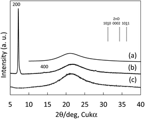 | ||
| Fig. 2 X-ray diffraction patterns for Ga:ZnO (a), CuPC (b), and CuPC:GZO-BHJ layers (c) prepared on quartz glass substrate. | ||
Fig. 3 shows topography and phase images taken for GZO, CuPC, and CuPC:GZO-BHJ layers prepared on quartz glass substrate with AFM. The GZO layer was composed of aggregate of granular grains with the size ranging from 15 to 30 nm, and the surface roughness (Ra) was estimated to be 2.1 nm from the topography image. The almost constant contrast was observed on the phase image over entire the GZO surface. The granular grains with the size of 35 to 50 nm were observed on the topography image for the CuPC layer, and the surface roughness (Ra) was estimated to be 7.2 nm. The phase image for the CuPC layer showed almost constant contrast over entire the CuPC surface.
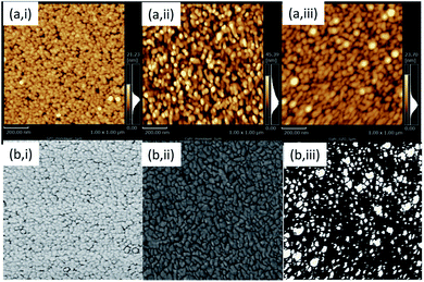 | ||
| Fig. 3 Topography (a) and phase images (b) taken with atomic force microscopy for Ga:ZnO (GZO) (i), CuPC (ii), and CuPC:GZO-BHJ layers (iii) prepared on quartz glass substrate. | ||
The CuPC:GZO-BHJ layer possessed aggregate of granular grains ranging from 30 to 50 nm in size, and the surface roughness (Ra) was estimated to be 2.2 nm from the topography image. The CuPC:GZO-BHJ layer showed bright and dark regions on the phase image. The phase contrast closely related to the micromechanical properties of component materials such as elastic property and strength,15,16 and the phase image is used for observing the distribution of components in nano-scale mixture of polymer materials with different micromechanical property. Both the elastic modulus and strength of the ZnO17 were higher than those for CuPC,18 and the relatively bright contrast was given by the GZO with high elastic modulus and strength. The bright part of the GZO component dispersed in the CuPC matrix, and the size estimated from the phase image ranged from 7 to 84 nm. Since the broadening of the diffracted X-ray peak identified as the CuPC component was calculated to be below 1 degree for the grain size of 10 nm, according to the Sherrer's equation, it was difficult to explain the disappearance of the diffracted X-ray peak identified as the CuPC component in the BHJ layer by the small grain size. Although further investigation is needed, the growth of the CuPC layer was interfered by the GZO component evaporated simultaneously, and the some amount of defects was introduced into the CuPC component, resulting in the disappearance of the diffracted X-ray peaks. The area ratio of the GZO component was estimated to be approximately 21% from the phase image. When the GZO component dispersed homogeneously throughout the BHJ layer, the volume fraction of the GZO component was calculated to be approximately 4%.
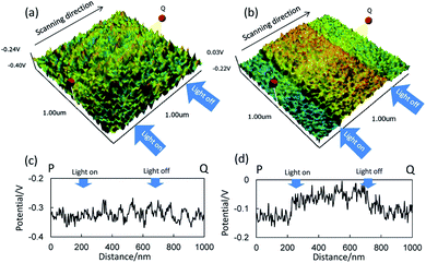
Fig. 4 shows images and line profiles of potential for CuPC and CuPC:GZO-BHJ layers prepared on the n-ZnO/FTO substrate with and without the light irradiation. The potential measured by KFM changed depending on the semiconductor type and dopant concentration due to the change in Fermi level. The measurement of the potential was used for estimating the built-in voltage formed at the heterointerface19,20 and photovoltage21 for Si diodes including Si solar cell. And, the diffusion length and life time of the minority carrier have been estimated with PKFM.22,23 The potential image was recorded by scanning the cantilever from the point P side to point Q side, and the distance from P to Q was 1000 nm. The line profiles represented the change in potential on the line from point P to point Q. The light irradiation was started at the distance of 250 nm from the P side and stopped at 700 nm.
The CuPC layer prepared on the n-ZnO/FTO substrate showed almost constant potential over the CuPC layer surface, although there was slight fluctuation. The light irradiation did not show any effect on the potential both on the image and line profile. On the contrast, the light irradiation induced the change in potential for the CuPC:GZO-BHJ layer prepared on the n-ZnO/FTO substrate. The potential changed rapidly by the light irradiation and showed almost constant potential during the light irradiation. And, the potential returned rapidly by stopping the light irradiation and kept almost constant value corresponding to that before the light irradiation.
Since the approximately 60% of the light irradiated from the glass substrate side reached to the free surface of CuPC and CuPC:GZO-BHJ layers from light absorption coefficients already calculated, the excitons was formed throughout the CuPC layer thickness. It was reported for the Si solar cell that the change in the potential measured by KFM was induced by light irradiation due to the change in free carrier.21 The diffusion length of exciton was reported to be approximately 10 nm for the vacuum-evaporated CuPC layer, and the dissociation of exciton to free carrier was occurred by the internal electric field at the heterointerface to inorganic semiconductor. The formation of free carrier was limited only within the region near the heterointerface to under n-ZnO layer, and the free carrier could not be formed near the free surface of the CuPC layer in spite of the formation of excitons, resulting in no change in the potential at the free surface.
The CuPC:GZO-BHJ layer was a mixture of CuPC and GZO components in nanoscale, and the boundary was dispersed throughout the BHJ layer including the region in the vicinity of the free surface in addition to the heterointerface to under n-ZnO layer. The change in potential indicated the change in amount of the free carrier and Fermi level near the free surface, and the boundary between CuPC and GZO components act as the heterointerface to dissociate the exciton to free carrier. The CuPC and Au layers were stacked on the CuPC:GZO-BHJ layer to construct the photovoltaic device. It is expected to improve the photovoltaic performance by using the CuPC:GZO-BHJ layer alternative to the simple CuPC layer to accelerate the dissociation of exciton to free carrier.
Fig. 5 shows field-emission scanning electron microscopy images of cross-sectioned structures for the hybrid CuPC/n-ZnO and CuPC/CuPC:GZO/n-ZnO photovoltaic devices. Both the CuPC and n-ZnO layers could be clearly observed between the Au and F:SnO2 (FTO) layers of the layered CuPC/GZO hybrid photovoltaic device. The CuPC and n-ZnO layers possessed a homogeneous thickness, but both layers possessed a slightly rough interface due to the surface irregularity of the FTO substrate. The n-ZnO layer was composed of aggregates of columnar grains grown in a direction nearly normal to the substrate surface, and the grain size was estimated to be approximately 136 nm. The CuPC layer was observed over entire the n-ZnO layer surface and was composed of granular grains with sizes ranging from 25 to 75 nm. The CuPC layer appeared slightly dark in the FE-SEM image compared to those for the n-ZnO and Au layers, and the interface to n-ZnO could be clearly observed on the image.
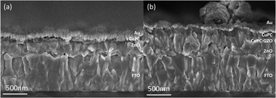 | ||
| Fig. 5 FE-SEM images for layered CuPC/n-ZnO (a) and CuPC/CuPC:GZO/n-ZnO hybrid photovoltaic devices (b). | ||
The 500 nm-thick-layer composed of the 200 nm-thick-CuPC:GZO BHJ and 300 nm-thick-n-ZnO layers was located between the CuPC and FTO layers of the CuPC/CuPC:GZO/n-ZnO hybrid photovoltaic device. The CuPC:GZO/n-ZnO layer was composed of aggregates of columnar grains grown in a direction nearly normal to the surface throughout the 500 nm thickness, and the interface between the n-ZnO and CuPC:GZO BHJ layers could not be observed. The CuPC layer was composed of the aggregate of columnar grains, and the interface between the CuPC and CuPC:GZO layers could be clearly observed due to the difference in contrast. The layered hybrid CuPC/n-ZnO and CuPC/CuPC:GZO/n-ZnO heterostructures prepared on the FTO substrate24 were characterized with X-ray diffraction measurement. (The diffraction patterns are not shown here; see ESI.†) The n-ZnO layer showed characteristic diffraction peaks, and the slight (0001) preferred orientation was observed from the peak intensity. The CuPC layer prepared on the n-ZnO layer showed the (200) peak for the characteristic monoclinic lattice, and the peak was disappeared for the CuPC:GZO-BHJ layer. The results were consistent to those prepared on the quartz glass substrate shown in Fig. 2.
Fig. 6 shows the current density–voltage curves for hybrid CuPC/n-ZnO and CuPC/CuPC:GZO/n-ZnO photovoltaic devices. The rectification ratio was estimated by calculating the current density ratio at the voltage of ±1 V. The forward current density was estimated to be the value at the forward voltage of 1 V. The ideality factor (η) was calculated using the following relation between the forward current density (JF) and forward voltage (VF);
| JF ∝ exp(qVF/ηKT) |
 | ||
| Fig. 6 Current density–voltage curves for layered CuPC/n-ZnO (a) and CuPC/CuPC:GZO/n-ZnO hybrid photovoltaic devices (b) in dark. | ||
The rectification feature was improved by inserting the CuPC:GZO-BHJ layer between the n-ZnO and CuPC layers, and the rectification ratio, forward current density, and ideality factor were estimated to be 51, 034, 44.4 mA cm−2, and 2.3, respectively. The forward current density was increased compared to that for the layered CuPC/n-ZnO photovoltaic device. The ideality factor was nearly close to 2 for the recombination current domination.
Fig. 7 shows the current density–voltage curves for the hybrid CuPC/n-ZnO and CuPC/CuPC:GZO/n-ZnO photovoltaic devices under AM1.5G illumination. The layered CuPC/n-ZnO photovoltaic device generated the photocurrent density of −4 × 10⁻⁴ mA cm−2 at 0 V by AM1.5G illumination. It was confirmed that the current density was very close to 0 mA cm−2 at 0 V in dark as shown in Fig. 6. The open-circuit voltage was very low, and the conversion efficiency was very low on the order of 10−7%, as already reported for the ZnO/H2PC photovoltaic devices.8
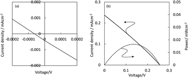 | ||
| Fig. 7 Current density–voltage and power–voltage curves for layered CuPC/n-ZnO (a) and CuPC/CuPC:GZO/n-ZnO hybrid photovoltaic devices (b) under AM1.5G illumination. | ||
The insertion of the CuPC:GZO-BHJ layer between the CuPC and n-ZnO layers induced an improvement in the photovoltaic performance. The short-circuit current density of 0.24 mA cm−2 was obtained for the hybrid CuPC/CuPC:GZO/n-ZnO photovoltaic device and was higher than that for the layered CuPC/n-ZnO photovoltaic device. The open-circuit voltage was estimated to be 0.26 V, and the conversion efficiency was calculated to be 0.017% from the FF value of 0.26.
The conversion efficiency of the layered H2PC/n-ZnO photovoltaic device increased by inserting the highly resistive ZnO buffer layer at the heterointerface, because that the recombination loss was suppressed by the conduction band offset formed between the H2PC and ZnO layers.8 The CuPC:GZO-BHJ layer showed very high resistivity over 108 Ωcm, suggesting that the CuPC:GZO-BHJ layer played a role like the ZnO buffer layer. The conversion efficiency of the CuPC/CuPC:GZO/n-ZnO hybrid photovoltaic device was approximately ten times that of the H2PC/ZnO-buffer/n-ZnO photovoltaic device, although the semiconductor materials were different, indicating the existence of the additional effect of the bulk-heterojunction (BHJ) structure. The concentration of the free carrier at the free surface corresponding to the interface in photovoltaic devices increased by using the CuPC:GZO-BHJ layer alternative to the CuPC layer, due to the existence of the heterointerface dispersed inside the BHJ-layer. This is a reason for the difference in conversion efficiency among the CuPC/CuPC:GZO/n-ZnO and H2PC/ZnO-buffer/n-ZnO photovoltaic devices.
4. Conclusions
The bulk-heterojunction (BHJ) layer composed of the Ga-doped ZnO (GZO) and the Cu-phthalocyanine (CuPC) semiconductors was prepared by the simultaneous evaporation system with the electron-beam evaporation for the GZO and the thermal evaporation for the CuPC. The hybrid CuPC/CuPC:GZO/n-ZnO photovoltaic device was constructed by electrodeposition of the n-ZnO layer in a simple zinc nitrate aqueous solution followed by the simultaneous evaporation. The CuPC:GZO-BHJ layer was a nano-scale mixture of both components with characteristic atomic arrangements, and the increase in the free carrier was induced by the bulk-heterojunction structure due to the increase in the heterointerface under light irradiation. The rectification feature with a 51![[thin space (1/6-em)]](https://www.rsc.org/images/entities/char_2009.gif) 034 in rectification ratio, 44 mA cm−2 in forward current density, and 2.3 in ideality factor was obtained for the hybrid CuPC/CuPC:GZO/n-ZnO photovoltaic device. The conversion efficiency was improved to 0.017% with the short-circuit current density of 0.24 mA cm−2 and open-circuit voltage of 0.26 V from 10−7% for the layered CuPC/n-ZnO photovoltaic device. The results demonstrated here indicated that the area and distribution of the heterointerface was an important parameter affecting the photovoltaic performance and the bulk-heterojunction structure is a realistic candidate as a next-generation thin film photovoltaic device.
034 in rectification ratio, 44 mA cm−2 in forward current density, and 2.3 in ideality factor was obtained for the hybrid CuPC/CuPC:GZO/n-ZnO photovoltaic device. The conversion efficiency was improved to 0.017% with the short-circuit current density of 0.24 mA cm−2 and open-circuit voltage of 0.26 V from 10−7% for the layered CuPC/n-ZnO photovoltaic device. The results demonstrated here indicated that the area and distribution of the heterointerface was an important parameter affecting the photovoltaic performance and the bulk-heterojunction structure is a realistic candidate as a next-generation thin film photovoltaic device.
Notes and references
- M. D. McGehee, MRS Bull., 2009, 34, 95 CrossRef CAS.
- W. J. E Beek, M. Wienk, M. Kemerink, X. Yang and R. A. J. Janssen, J. Phys. Chem. B, 2005, 109, 9505 CrossRef PubMed.
- K. M. Coakley and M. D. McGehee, Appl. Phys. Lett., 2003, 83, 3380 CrossRef CAS.
- C. Tang, Appl. Phys. Lett., 1986, 48, 183–185 CrossRef CAS.
- M. Izaki, T. Saito, T. Ohata, K. Murata, B. M. Fariza, J. Sasano, T. Shinagawa and S. Watase, ACS Appl. Mater. Interfaces, 2012, 4, 3558 CAS.
- M. Izaki, T. Shinagawa, K. Mizuno, Y. Ida, M. Inaba and A. Tasaka, J. Phys. D: Appl. Phys., 2007, 40, 3326 CrossRef CAS.
- K. Sakai and M. Hiramoto, Mol. Cryst. Liq. Cryst., 2008, 491, 284 CrossRef CAS.
- M. Izaki, R. Chizaki, T. Saito, K. Murata, J. Sasano and T. Shinagawa, ACS Appl. Mater. Interfaces, 2013, 5, 9386 CAS.
- Y. Terao, H. Sasabe and C. Adachi, Appl. Phys. Lett., 2007, 90, 103515 CrossRef.
- S.-G. Ihn, K.-S. Shin, M.-J. Jin, X. Bulliard, D. Yun, Y. S. Choi, Y. Kim, J.-H. Park, M. Sim, M. Kim, K. Cho, T. S. Kim, D. Choi, J.-Y. Choi, W. Choi and S.-W. Kim, Sol. Energy Mater. Sol. Cells, 2011, 95, 1610 CrossRef CAS.
- T. Javier and R. Garcia, Appl. Phys. Lett., 1997, 71, 2394 CrossRef.
- L. Wang, Appl. Phys. Lett., 1998, 73, 3781 CrossRef CAS.
- R. Seoudi, G. El-Bahy and Z. El Sayed, Opt. Mater., 2006, 29, 304 CrossRef CAS.
- C. Brown, J. Chem. Soc. A, 1968, 2488 RSC.
- J. Tamiya and R. Garcia, Appl. Phys. Lett., 1997, 71, 2394 CrossRef.
- S. Ahnh, S. A. Chizhik, A. M. Dubravin, V. P. Kazachenko and V. V. Popov, Wear, 2001, 249, 617 CrossRef.
- S.-R. Jian, I.-J. Teng, P.-F. Yang, Y.-S. Lai, J.-M. Lu, J.-G. Chang and S.-P. Ju, Nanoscale Res. Lett., 2008, 3, 186 CrossRef CAS.
- M. Kamari, Y. Karino and T. Wakamatsu, Jpn. J. Appl. Phys., 2005, 44, 8249 CrossRef.
- A. Kikukawa, S. Hosokawa and R. Imura, Appl. Phys. Lett., 1995, 66, 3510 CrossRef CAS.
- R. Shikler, T. Meode, N. Fried and Y. Rosenwaks, Appl. Phys. Lett., 1999, 74, 2972 CrossRef CAS.
- M. Takikawa, T. Igarashi, T. Ujihara and T. Takahashi, Jpn. J. Appl. Phys., 2007, 46, 5548 CrossRef.
- M. Takikawa, T. Igarashi and T. Ujihara, Appl. Phys. Lett., 2009, 95, 191908 CrossRef.
- M. Takikawa, T. Igarashi and T. Ujihara, Appl. Phys. Lett., 2008, 93, 021902 CrossRef.
- Joint Comittee on Powder Diffraction Standards, Powder Diffraction File, 41–1445, International Data for Diffraction Data, Swartthmore, PA, 1992 Search PubMed.
- S. M. Sze and K. K. Ng, Physics of Semiconductor Devices, Wiley-Interscience, New Jersey, 3rd edn, 2007, p. 99 Search PubMed.
Footnote |
| † Electronic supplementary information (ESI) available: Schematic diagram of the hybrid photovoltaic devices with and without GZO:CuPC-bulk-heterojunction (BHJ) layer. Schematic illustration of photo-assisted kelvin force microscopy. X-ray diffraction patterns for layered CuPC/n-ZnO and CuPC/CuPC:GZO/n-ZnO hybrid photovoltaic devices prepared on FTO substrate. See DOI: 10.1039/c4ra01051e |
| This journal is © The Royal Society of Chemistry 2014 |

