Chemical vapor deposition of diamond on an adamantane-coated sapphire substrate

Yi-Chun Chen and Li Chang*
Department of Materials Science and Engineering, National Chiao Tung University, 1001, Tahsueh Road, Hsinchu, Taiwan 300, Republic of China. E-mail: lichang@cc.nctu.edu.tw; Fax: +886-3-5724727; Tel: +886-3-5731615

Received 6th February 2014 , Accepted 10th April 2014

First published on 10th April 2014


Abstract

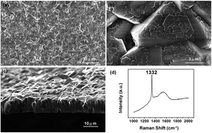
Continuous diamond thin films can be grown on sapphire substrates by microwave plasma chemical vapor deposition utilizing a pretreatment of adamantane dip coating on the substrate for enhanced nucleation. Scanning electron microscopy, X-ray diffraction and Raman spectroscopy show that 〈111〉 oriented diamond films of good crystallinity can be deposited on adamantane-coated sapphire substrates. Cross-sectional transmission electron microscopy at the diamond/sapphire interface shows that diamond can be directly synthesized on sapphire without any interlayer.


Introduction

The synthesis of diamond films by chemical vapor deposition (CVD) has been widely demonstrated in the past few decades due to the outstanding physical and chemical properties of diamond for various technological applications.1–4 In particular, the growth of continuous diamond thin films on optically transparent and hard substrates, such as sapphire, is important for the development of corrosion resistance and infrared windows.5 Diamond growth on sapphire has been studied in the past. Yoshimoto et al. have reported the nucleation and growth of diamond crystallites on sapphire by pulsed laser deposition (PLD).6 Chen et al. also studied the PLD growth mechanism of diamond on sapphire.7 Several studies for diamond growth used hot-filament chemical vapor deposition method with scratching pretreatment on sapphire to increase the nucleation density.8–10 Also, there are a few studies of the growth of diamond on sapphire coated with a buffer layer of platinum and iridium.11–13 However, the growth of diamond films on optically transparent substrates like sapphire has to address several issues. For diamond growth on polished and smooth sapphire wafers, diamond nucleation is one of the most critical issues. Conventional pretreatment methods for nucleation enhancement include mechanical scratching and dc-biasing. Scratching will damage the surface of the substrate and degrade the optical properties, which is unsuitable for transparent sapphire for high performance devices. Although Williams, et al.33 have used the ultrasonic seeding with nanodiamond for pretreatment procedure to grow the diamond film, it has not been shown if oriented diamond films can be obtained. For the dc-biasing method which has been successfully used to grow diamond directly on mirror-polished Si wafers for enhanced nucleation, it is not possible to apply to the insulting sapphire. Another critical issue for diamond growth on sapphire is that there is large thermal mismatch between diamond and sapphire due to the significant difference in their coefficients of thermal expansion, resulting in very high compressive stresses in the thin film.14,15 In general, the crystallinity of a diamond film can be improved with increasing film thickness and growth temperature; however, the thermal stress also increases with the thickness and the growth temperature. To obtain high quality diamond on sapphire, the film thickness will be limited by the stress which may causes cracking or delamination. Nevertheless, Singh et al. showed that low temperature growth can obtain adherent diamond films on optically transparent sapphire.23 Several approaches, such as utilizing in situ two-step hot filament chemical vapor deposition or polishing the substrate surface carefully and by in situ pre-deposition of a carbon layer on the alumina substrate surface, or using the activated species transport (AST) method which supplies activated diamond species to the substrate in a plasma flame, were proposed to overcome the problem, but they still resulted in a relatively low nucleation density (∼106–107 particles per cm2).16–20

We have previously shown enhanced nucleation of diamond on adamantane-coated Si at relatively low temperatures21,22 which may mitigate the thermal stress. In this work, we report the application of a pretreatment method of adamantane coating on sapphire substrate for diamond film growth by chemical vapor deposition (CVD).

Adamantane (C10H16) consists of 10 carbon atoms arranged as a single diamond cage surrounded by 16 hydrogen atoms. The spatial arrangement of carbon atoms in adamantane molecule is the same as that in diamond crystal. In other words, an adamantane molecule can be regarded as a sub-nanometer sized unit of diamond crystal. Here, we show that coating of adamantane on sapphire can be an effective method to grow diamond on flat sapphire surface.

Experimental

Commercially available 2-inch c-plane sapphire wafers were cut into a dimension of 1 × 1 cm2 as substrate. The substrates without any mechanical pretreatment were ultrasonically cleaned with acetone for 10 minutes, and dried with nitrogen gas. Then, the substrates were dip-coated in an ethylene glycol solution with adamantane powder (purity >99%) at room temperature. The glycol has been proved to be effective to reduce the evaporation of adamantane which has a high vapor pressure at room temperature.22 The concentration of the solution was 1 g adamantane per 10 ml solvent. The dip coating conditions were similar to those used for Si substrate which had been described in detail elsewhere.22

The adamantane-coated sapphire substrates were placed on a Mo holder for diamond growth in an AsTeX-type MPCVD system.24 The diamond films were grown at a gas pressure of 50 torr and microwave power of 800 W for various periods from 15 min to 48 h. The diamond films were formed at a fixed total gas flow rate of 300 sccm and in the gas mixture containing H2 and CH4 with a CH4–H2 ratio of 0.3/99.7. The substrate temperature during the deposition was roughly estimated to be 700 °C as measured by optical pyrometer.

The surface morphology was examined in a field emission scanning electron microscope (SEM, JEOL JSM-6500F). The crystallinity of diamond was evaluated with X-ray diffraction (XRD) and Raman spectroscopy. XRD patterns were acquired from a Bruker D2 XRD system using Cu Kα X-rays. Raman spectroscopy was performed in a LABRAM HR800 system, which allowed the 488 nm laser beam be focused to 1 μm diameter for micro-mode operation. The film microstructure and the interface were characterized using transmission electron microscopy (TEM, FEI Tecnai30F operated at 300 kV). Focused ion beam (FIB, Seiko Instruments SMI 3050SE) was used for cross-sectional TEM specimen preparation.

Results and discussion

After dip-coating of adamantane on sapphire substrate, the adamantane-coated sapphire substrates were placed in a MPCVD reactor for diamond deposition. Fig. 1(a) shows the top view surface morphologies of a deposited diamond film on the sapphire substrate after 48 h growth. The diamond grains have an average size in ∼10 μm. In the high magnification image as shown in Fig. 1(b), it can be clearly seen that the surface morphology of the synthesized diamond exhibits triangular and hexagonal shapes which are the typical appearance of diamond {111} facets. The thickness of the continuous diamond film is ∼10 μm as shown in Fig. 1(c) in cross section view, giving the growth rate of diamond of 0.2 μm h−1. Fig. 1(d) shows a Raman spectrum of the diamond film on sapphire. The Raman peak at 1332 cm−1 confirms the successful deposition of the diamond film on sapphire, and the full width at half-maximum (FWHM) of the peak is determined to be 8 cm−1, implying a good crystallinity for the film. A broad band exists at ∼1550 cm−1 with a relatively lower intensity, suggesting the presence of a small amount of graphite. To make sure the effectiveness of adamantane dip coating for diamond nucleation, we have grown the diamond on the sapphire without coating adamantane under the same deposition condition for comparison. Also, to distinguish the role of adamantane from glycol on diamond nucleation in synthesis, we have examined the surface morphology of the substrate dip-coated in the pure solvent without any addition of adamantane after diamond deposition in the same MPCVD condition. The morphology on sapphire without coating adamantane is shown in Fig. 2(a) that most of the areas are rarely observed with diamond particles. The morphology of sapphire covered with dry-coated adamantane powder and the morphology of sapphire only dip-coated with glycol solvent without any addition of adamantane are shown as Fig. 2(b) and (c). Thus, it clearly indicates that the adamantane coating can enhance the yield of diamond deposition. However, we have no clear clues about whether adamantane directly transforms to diamond or decompose into carbon-containing radicals.
image file: c4ra01042f-f1.tif
Fig. 1 SEM images of synthesized diamond films on sapphire for 48 h in (a) low magnification in plan-view, and (b) high magnification in plan-view, and (c) in cross section. (d) Raman spectrum.

image file: c4ra01042f-f2.tif
Fig. 2 SEM surface morphology after CVD (a) on uncoated sapphire, (b) on sapphire cover with dry-coated adamantane powder, and (c) on sapphire only dip-coated with glycol solvent without any addition of adamantane.

To understand the evolution of the diamond deposition on adamantane-coated sapphire substrate, the deposition time was varied from 15–360 min with the same plasma condition. The SEM surface morphologies are shown in Fig. 3. For the 15 min deposition, only a few diamond particles in 1–2 μm size are seen to form on sapphire (Fig. 3(a) and (b)) from which the nucleation density is estimated to be about 1 × 107 cm−2. In Fig. 3(c) and (d), the number of diamond particles significantly increases after deposition for 30 min (the nucleation density ∼1 × 108 cm−2), indicating that the diamond nucleation density still increases with deposition time. After deposition for about 60 min, a continuous diamond film can form in some local areas. For the 360 min growth, a continuous diamond film has formed on the whole surface of sapphire substrate. The samples deposited for 15–360 min were also evaluated with Raman spectroscopy as shown in Fig. 4. In all cases, the diamond peak at 1332 cm−1 is clearly observed in addition to the disordered graphitic peak at 1580 cm−1. For the 15 min deposition, a weak peak at 1150 cm−1 is additionally observed, which can be attributed to the nanodiamond signal.25,26 Fig. 5 shows XRD patterns of the diamond films grown on sapphire for the different deposition times. In addition to sapphire (0006) peaks, the XRD patterns in Fig. 5 present sharp and well-defined peaks at 2θ = 43.9 and 75.7° corresponding to diamond {111} and {220} reflections, respectively, for growth time reaching 60 min and above, indicating that the deposited amount of diamond is increased above the detection limit of XRD in consistence with SEM observations.


image file: c4ra01042f-f3.tif
Fig. 3 SEM of diamond films on sapphire for different growth time in plan-view on the left column and cross-section view on the right column (a) and (b) 15 min, (c) and (d) 30 min, (e) and (f) 60 min, (g) and (h) 120 min, and (i) and (j) 360 min.

image file: c4ra01042f-f4.tif
Fig. 4 Raman spectra of diamond films on sapphire for 15–360 min growth.

image file: c4ra01042f-f5.tif
Fig. 5 XRD patterns of diamond films grown on sapphire for growth from 15 min to 48 h.

Furthermore, the cross-sectional TEM specimen of a diamond sample deposited on sapphire for 2 h was prepared by FIB. For the protection of the TEM specimen against damage from the high-energy ion beam in FIB, the specimen was coated with platinum before FIB cutting. The cross-sectional bright-field TEM image and the selected area electron diffraction (SAED) pattern from the marked regions of diamond and sapphire are shown in Fig. 6. The TEM image in Fig. 6(a) shows that the diamond crystallite is in twin characteristics for the left and right halves which also can be identified from the SAED patterns in Fig. 6(b)–(e) from the individual regions in Fig. 6. Also, it can be seen that the sapphire surface remains smooth after diamond deposition, implying that the sapphire has undergone negligible etching by the plasma. The SAED patterns in Fig. 6(b)–(d) obtained from the corresponding marked regions show the single crystalline diamond characteristics in 〈110〉 zone axis and sapphire in 〈2[1 with combining macron][1 with combining macron]0〉 one. The SAED patterns in Fig. 6(b) and (c) indicate that the left diamond is 〈001〉 oriented and the right one is 〈111〉 oriented, and they are in the twin relationship. The SAED pattern in Fig. 6(e) from the interface region shows that the orientation relationship is closed to 〈110〉 diamond//〈2[1 with combining macron][1 with combining macron]0〉 sapphire and {111} diamond//{0001} sapphire or {111} diamond//{0[1 with combining macron]14} sapphire. This is different from the in-plane epitaxial relationship of 〈110〉 diamond//〈1[1 with combining macron]00〉 sapphire which has been reported in literature.6,27,28 The lattice mismatch of diamond along 〈110〉 with sapphire along 〈2[1 with combining macron][1 with combining macron]0〉 is about 6% (5.04 Å versus 4.76 Å), in comparison with that of ∼39% with sapphire along 〈1[1 with combining macron]00〉 (8.24 Å). Only reflections of diamond and sapphire can be observed in Fig. 6(e) without any other additional diffraction reflections, suggesting that no crystalline interlayers exist between them and no extra crystalline phases in diamond. The HRTEM image in Fig. 6(f) is obtained from an interfacial region between diamond and sapphire (the left-hand side region of the image with zone axis in 〈2[1 with combining macron][1 with combining macron]0〉 sapphire), showing diamond and sapphire lattice fringes. The d-spacing between the fringes in the diamond region is 2.06 Å which corresponds to be the diamond {111} interplanar spacing, consistent with the SAED observations as shown in Fig. 6(b). As the diamond fringes are in connection with the sapphire ones, we can observe no interlayer formed between the diamond and the sapphire, suggesting that the diamond film was directly grown on the sapphire. As shown in Fig. 6(g), the filtered image after inverse fast Fourier transform (FFT) of the lattice image using diamond (111) and sapphire (0[1 with combining macron]14) reflections illustrates a reasonably good match of diamond (111) with sapphire (0[1 with combining macron]14) due to their close domain matching in 5[thin space (1/6-em)]:[thin space (1/6-em)]4 (d-spacings 2.06 Å vs. 2.55 Å), consistent with the result obtained from the SAED pattern in Fig. 6(e). Such domain matching has been often found in heteroepitaxy of thin film growth.29 Thus, it is suggested that diamond can be epitaxially grown on sapphire.


image file: c4ra01042f-f6.tif
Fig. 6 The cross-sectional BF-TEM image of diamond on sapphire and the corresponding SAED patterns from diamond and sapphire regions. (a) BF TEM, (b) and (c) SAED patterns of diamond from left and right hand sides, respectively, (d) SAEDP of sapphire. (e) SAEDP at the diamond/sapphire interface, (f) HRTEM image of the interface between diamond (left) and sapphire with (g) inverse FFT-filtered image of diamond (111) and sapphire (0[1 with combining macron]14).

Although Tiwari et al.30 have proposed the hydrogen abstraction as one of the possible mechanisms for diamond nucleation in the gas phase sublimated and mixed in the gaseous plasma which then deposited on the Si surface, it is worthwhile to briefly discuss the possible mechanisms for diamond nucleation and growth from adamantane on sapphire. It has been suggested that adamantane might be able to serve as embryo for nucleation of diamond in the gas phase as adamantane is easily evaporated at high temperature and decompose into individual molecules.21,31 When adamantane was in touch with plasma from gaseous (0.3% CH4 in H2) phase, it might decompose into hydrocarbon species. These species might convert to nanosized diamond particles in the gas phase. Then the particles deposited on the substrate surface might act as nuclei for subsequent growth of diamond on sapphire. Additionally, the hydrogen abstraction can be one of the possible mechanisms for diamond nucleation in the gas phase as adamantane can be considered as diamond nucleus covered with hydrogen atoms, and then methane gas species in hydrogen plasma may facilitate the growth of three dimensionally individual nuclei.30 Alternatively, some residual adamantane left on the substrate surface might be able to be directly converted to nanodiamond. Our previous study have shown that adamantane can adhere on Si though the OH-bond of glycol.22 Toshinari et al.32 have coated octadecyltrichlorosilane on the (0001) sapphire. It shows that the octadecyltrichlorosilane is covalently bound to the OH-terminated surface of sapphire. Therefore, the adamantane in glycol may bond with sapphire by C10H16–OH–O–Al bonds similar to the bonding on Si. As a result, the sticking of adamantane with the sapphire surface is enhanced, and its evaporation or sublimation is reduced, which can increase the chance for adamantane to remain on the surface and act as embryo for diamond nucleation.

Conclusions

In summary, we demonstrate a simple method for the direct synthesis of good quality and highly crystalline diamond films on adamantane-coated sapphire substrate by microwave plasma chemical vapor deposition. The results from SEM, XRD, and Raman spectroscopy show that the adamantane assists the diamond nucleation and a 〈111〉 oriented continuous diamond film on sapphire can be obtained. TEM examinations with electron diffraction analysis also confirm that the interface between diamond and sapphire is smooth with no interlayer formation, and an orientation relationship of diamond with sapphire is identified as 〈110〉 diamond//〈2[1 with combining macron][1 with combining macron]0〉 sapphire and {111} diamond//{0001} sapphire.

Acknowledgements

The authors would like to thank the National Science Council of the Republic of China, Taiwan, for financially supporting this research under contract NSC 101-2221-E-009-049-MY3.

References

  1. S. D. Wolter, M. T. McClure, J. T. Glass and B. R. Stoner, Appl. Phys. Lett., 1995, 66, 2810 CrossRef CAS PubMed.
  2. A. A. Fokin, B. A. Tkachenko, N. A. Fokina, H. Hausmann, M. Serafin, J. E. P. Dahl, R. M. K. Carlson and P. R. Schreiner, Chem.–Eur. J., 2009, 15, 3851 CrossRef CAS PubMed.
  3. H. G. Chen and L. Chang, Diamond Relat. Mater., 2009, 18, 141 CrossRef CAS PubMed.
  4. N. Yang, H. Uetsuka, E. Osawa and C. E. Nebel, Angew. Chem., Int. Ed., 2008, 47, 5183 CrossRef CAS PubMed.
  5. J. I. Pankove and C.-H. Qui, Synthetic Diamond: Emerging CVD Science and Technology, ed. K. E. Spear and J. P. Dismukes, Wiley, New York, 1994, pp. 401–418 Search PubMed.
  6. M. Yoshimoto, K. Yoshida, H. Maruta, Y. Hishitani, H. Koinuma, S. Nishio, M. Kakihana and T. Tachibana, Nature, 1999, 399, 340 CrossRef CAS PubMed.
  7. Z. Y. Chen, J. P. Zhao, T. Yano and J. Sakakibara, Phys. Rev. B: Condens. Matter Mater. Phys., 2000, 62, 7581 CrossRef CAS.
  8. H. W. Chen and V. Rudolph, Diamond Relat. Mater., 2003, 12, 1633 CrossRef CAS.
  9. O. Ternyak, R. Akhvlediani and A. Hoffman, Diamond Relat. Mater., 2005, 14, 323 CrossRef CAS PubMed.
  10. K. G. Saw and J. du Plessis, J. Cryst. Growth, 2005, 279, 349–356 CrossRef CAS PubMed.
  11. Z. Dai, C. Bednarski-Meinke and B. Golding, Diamond Relat. Mater., 2004, 13, 552 CrossRef CAS PubMed.
  12. A. Samotoa, S. Itoa, A. Hotta, T. Hasebe, Y. A. Sawaabe and T. Suzuki, Diamond Relat. Mater., 2008, 17, 1039 CrossRef PubMed.
  13. T. Tachibana, Y. Yokota, K. Kobashi and M. Yoshimoto, J. Cryst. Growth, 1999, 205, 163 CrossRef CAS.
  14. M. D. Drory and J. W. Hutchinson, Science, 1994, 263, 1753 CAS.
  15. R. Ramesham and T. Roppel, J. Mater. Res., 1992, 7, 1144 CrossRef CAS.
  16. Y. Zhang, L. Xie, Z. H. Zhou, J. Sun and S.-T. Lee, J. Cryst. Growth, 1996, 169, 722 CrossRef CAS.
  17. A. V. Sumant, V. P. Godbole and S. T. Kshirsagar, Mater. Sci. Eng., B, 1996, 39, L5 CrossRef.
  18. Y. Mo, Y. Xia and W. Wu, J. Cryst. Growth, 1998, 191, 459 CrossRef CAS.
  19. X. Qiao, O. Fukunaga, N. Shinoda and K. Yui, Diamond Relat. Mater., 1996, 5, 1096 CrossRef CAS.
  20. Z. Fang, Y. Xia, L. Wang, Z. Wang, W. Zhang and Y. Fan, J. Phys. D: Appl. Phys., 2002, 35, L57 CrossRef CAS.
  21. R. N. Tiwari, J. N. Tiwari and L. Chang, Chem. Eng. J., 2001, 158, 641 CrossRef PubMed.
  22. Y. C. Chen and L. Chang, RSC Adv., 2013, 3, 1514 RSC.
  23. R. K. Singh, D. R. Gilbert and J. Laveige, Appl. Phys. Lett., 1996, 69, 2181 CrossRef CAS PubMed.
  24. K. Kobashi, Diamond films: chemical vapor deposition for oriented and heteroepitaxial growth, 2005, ch. 3, pp. 17–22 Search PubMed.
  25. A. C. Ferrari and J. Robertson, Phys. Rev. B: Condens. Matter Mater. Phys., 2001, 63, 121405 CrossRef.
  26. T. Hirai, Y. Kanno and Y. Takagi, Jpn. J. Appl. Phys., 2008, 47, 738 CrossRef CAS.
  27. M. Yoshimoto, M. Furusawa, K. Nakajima, M. Takakura and Y. Hishitani, Diamond Relat. Mater., 2001, 10, 295 CrossRef CAS.
  28. G.-S. Park, S. C. Bae, S. Granick, J.-H. Lee, S.-D. Bae, T. Kim and J. M. Zuo, Diamond Relat. Mater., 2007, 16, 397 CrossRef CAS PubMed.
  29. J. Narayan and B. C. Larson, J. Appl. Phys., 2003, 93, 278 CrossRef CAS PubMed.
  30. R. N. Tiwari and L. Chang, Appl. Phys. Express, 2010, 3, 045501 CrossRef.
  31. M. Umeno, M. Noda, H. Uchida and H. Takeuchi, Diamond Relat. Mater., 2008, 17, 684 CrossRef CAS PubMed.
  32. T. Isono, T. Ikeda, R. Aoki, K. Yamazaki and T. Ogino, Surf. Sci., 2010, 604, 2055 CrossRef CAS PubMed.
  33. O. A. Williams, M. Daenen, K. Haenen, E. Osawa and M. Takahashi, Chem. Phys. Lett., 2007, 445, 255 CrossRef CAS PubMed.

This journal is © The Royal Society of Chemistry 2014
Click here to see how this site uses Cookies. View our privacy policy here.