Digitally-patterned nanoprobe arrays for single cell insertion enabled by wet tapping

Yoon Ho Seoa, Lo Hyun Kima, Fritz B. Prinzb and WonHyoung Ryu*a
aSchool of Mechanical Engineering, Yonsei University, 50 Yonsei-ro, Seodaemun-gu, Seoul 120-749, Republic of Korea. E-mail: whryu@yonsei.ac.kr
bDepartment of Mechanical Engineering, Stanford University, California 94305, USA

Received 2nd February 2014 , Accepted 24th March 2014

First published on 25th March 2014


Abstract

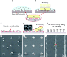
Wet tapping of nanoparticles for precisely-patterned nanoprobe arrays was developed to fabricate cell insertion tools for parallel multiple cell probing. Simple and scalable patterning of nanoparticles with patterning yield higher than 98% on a photoresist template was achieved by wet tapping. The effect of tapping time, particle materials, particle concentration, and surface conditions on the wet tapping was analyzed. Using the patterned nanoparticles, arrays of precisely-patterned nanoprobes were created. For cellular probing at single cell resolution, insertion of a controlled number of nanoprobes into single algal cells in a parallel fashion was also demonstrated.


For intracellular probing, high aspect-ratio (A/R) nanostructures such as nanowires (NWs) are ideal since they can be inserted into living cells without damaging cell membranes. Thus, vertically-aligned nanoprobes (VNPs) have been developed as sensors to monitor biophysical or biochemical activities in the vicinity or the inside of living cells.1–4 For parallel intracellular sensing that uses multiple nanoprobes, an array of multiple nanoprobe-type sensors are required for registered recording of biosignals from each cell. However, fabrication of VNPs with high A/R in an array form is non-trivial and it requires expensive fabrication processes such as E-beam lithography (EBL)5,6 or epitaxial growth.7–9 In our previous study, we demonstrated heterogeneous nanosphere lithography (HNSL) to construct an array of spacing-controlled VNPs for multiple cellular probing.10 However, random spacing between VNPs by the HNSL limits the design of electrode connection for signal recording from each VNP sensor.

As a means to control the self-assembled locations of nanoparticles, a template-based self-assembly technique was introduced.11–13 The techniques used a capillary force to bring nanoparticles into the template and the particles were patterned by developing the photoresist (PR) template. However, the nanoparticle patterned by a capillary force is rather a slow process for patterning large surfaces and it requires highly-precise control of capillary angle, drawing speed, and environmental factors such as temperature and humidity. Recently, dry manual patterning of nanoparticles was demonstrated as a simpler way to achieve nanoparticle patterning, using nano templates and adhesive material.14 However, adhesive removal at a high temperature is incompatible with polymer and metal nanoparticles, which limits broader application of the method. Although such template-based patterning of nanoparticles overcame many obstacles in assembly of nanoparticles, an efficient way to assemble nanoparticles into each nano or micro-patterns in a template is still required.

In this study, we developed a fast and simple patterning of nanoparticles at pre-determined locations to fabricate precisely-patterned VNPs. Instead of relying on previously-mentioned capillary force or adhesives, we demonstrated that simple “physical push and fill” of particles in a particle solution assembled individual nanoparticles in patterned cavities with high efficiency. Two “physical push and fill” methods, doctor-blading and tapping of nanoparticle solutions, were investigated and evaluated compared to the capillary assembly method. We also studied several key parameters of this “physical push and fill” method including particle material, tapping time, cavity geometry, particle concentration, and surface condition to understand the basic mechanism of the proposed approach. Finally, we demonstrated that the patterned arrays of nanoparticles on a silicon substrate were utilized as etch masks to create arrays of vertically-aligned nanoprobes as cell probing tools. Using an algae, Chlamydomonas reinhardtii (chlamy cell), and a custom-built cell probing station, insertion of a single or multiple nanoprobes into a single algal cell was demonstrated.

Polystyrene (PS) and silica nanoparticles were used as etch masks for fabrication of a nanoprobe array in this study. The wet tapping process consisted of two steps: (1) dispensing nanoparticle solution on a patterned photoresist (PR) template (Fig. 1a and 2) tapping the particle solution into the cavity patterns using polyurethane (PU) swab (Fig. 1b). These two steps were repeated until all the PR patterns were filled by the particles. Excessive particles on the templates remained and they were removed by gentle cleaning using the PU swab soaked with water to minimize any damage to the surface of PR templates (Fig. 1c and d). By either developing PR in an organic solvent or dry etching, the patterned nanoparticles were left on the silicon substrate. Subsequent deep reactive ion etching (DRIE) produced a patterned array of VNPs with high aspect ratio (Fig. 1e). Finally, the patterned VNP array was inserted into single algal cells to confirm that the nanoprobe could penetrate the cell membrane without breaking the intact cell structure.


image file: c4ra00940a-f1.tif
Fig. 1 Schematic diagram of wet tapping for the fabrication of patterned VNP array. (a) Nanoparticle solution dispensed on Si substrate with patterned templates. (b) Loading of nanoparticles into the templates by tapping nanoparticle solution. (c) Excessive particles residue on the templates. (d) Cleaning process of excess particles on the templates. (e) Removal of the template and fabrication of patterned NW arrays using DRIE process. (f)–(h) Scanning electron microscope images of each steps corresponding to (c)–(e).

image file: c4ra00940a-f2.tif
Fig. 2 Schematic diagrams of nanoparticle patterning using (a) capillary assembly, (b) doctor-blading, and (c) wet tapping. SEM images (d)–(f) of patterned particles by each technique corresponding to (a)–(c). Inset figure in (e) is zoomed-in view of crushed PR pattern (location indicated by red arrow). (g) Loading yield comparison of PS and silica nanoparticles in patterned cavities for each loading technique. (h) Average loading yield of PS nanoparticles in patterned cavities for concentrations of particle solution.

For efficient nanoparticle patterning, capillary-induced loading of nanoparticles was investigated. First, a droplet of nanoparticles solution was dispensed on a template which was treated by oxygen plasma. Evaporation of the solvent at room temperature induced capillary-driven transport of the nanoparticles and loaded the cavity patterns slowly (Fig. 2a). Then excessive particles were cleaned by PU swab without disrupting loaded particle since the height of PR template was identical to the diameter of nanoparticles. Fig. 2d shows the nanoparticles loaded in patterned cavities by capillary loading. However, this approach showed relatively low loading yield of about 22% for PS particles and 40% for silica particles, respectively. The loading yield was defined as the ratio of a number of loaded particles to total number of particles that could be loaded and fill the cavities.

As mentioned in previous studies, particle placement in geometric confinement is governed by a collective effect of evaporation, capillary effect, gravity, and surface geometry.12,13 There usually exists a very narrow range of such operation parameters that allows the particle placement in nano or micro patterns. It is also noteworthy that PS particles have lower efficiency than silica particles in loading micro cavities. This is ascribed to the lower specific gravity of the PS particles than silica particles, since gravitational assembly is more efficient with particles with higher specific gravity in bringing particles into geometrically-confined space.12

Although the dry manual assembly is an effective method to pattern nanoparticles, handling of nanoparticles at a dry environment is less desirable and the calcine step at high temperature to remove adhesive materials is incompatible with most polymer or metal particles. Instead, we attempted doctor-blading of nanoparticles in a solution (“wet doctor-blading”) to physically force the nanoparticles into cavity patterns. A droplet of a nanoparticle solution was dispensed on a PR template. Then, the template was doctor-bladed using PU swab (Fig. 2b). A commercial PU swab was used as a tool for doctor-blading (Fig. 1b). This doctor-blading technique showed higher yield of about 67% than the capillary-driven patterning (Fig. 2e and g). Interestingly, the loading yield difference between PS and silica particles was much smaller than the capillary-based loading. This can be explained by the minimized role of gravity-based assembly in this “wet” doctor-blading that utilized a physical force to load nanoparticles in patterned cavities.

During doctor-blading, however, PR templates were often damaged and deformed due to friction between PU swab and template surface. Often, crushed PR filled the cavity patterns or formed thin membranes on nanoparticles, hindering further loading of nanoparticles into the cavities (Fig. 2e). In addition, such PR residue was detrimental to subsequent dry etching steps to fabricate vertical nano pillar shapes. Even, an additional step of dry etching failed to remove the PR residue completely.


image file: c4ra00940a-f3.tif
Fig. 3 (a) Schematic diagrams of wet tapping over time and the corresponding images of each step of wet tapping. (b)–(d) SEM images of arrays of patterned PS particles after wet tapping. (e)–(g) SEM images of patterned silica particles using templates of various shapes.

For improved loading of nanoparticles without damage to PR surfaces, “wet tapping” was developed. In contrast to the previous methods, the wet tapping was performed by gentle tapping of a particle solution only in a vertical direction (Fig. 2c). Vertical moving of a PU swab minimized friction between the PU swab and PR template surfaces, leading to minimal damage to PR surfaces (Fig. 2f). This wet tapping improved the loading yield dramatically up to about 93% over a large surface (Fig. 2g). With high loading uniformity, the method was scalable to any size of silicon substrate. Since this also relied on physical force rather than gravitational force, the difference in loading yield between PS and silica particles was negligible. In order to understand the effect of tapping time on loading efficiency, tapping time was increased from 10 to 15 min. This tapping for an extended period produced the loading of nanoparticles with loading yield higher than 98%. The remaining 2% of unloaded particles was caused by misfit size of nanoparticles since the nanoparticles were provided with a size distribution.

On the other hand, the particle concentration of the solution also had a significant impact on the quality of particle patterning. The concentrations were varied from 2.5 to 0.001% (w/v) by diluting particle solutions with deionized water. As shown in Fig. 2h, the loading yields were higher than 90% until the solution concentration decreased down to 0.1%. Interestingly, the loading yield drastically dropped below the concentration of 0.05%. To explain this, we assumed that about 10 μL of a particle solution was dispensed on a substrate of 5 × 5 mm2. Spacing between each cavity was 10 μm and each cavity needed four particles for complete loading. With these conditions, a minimum concentration of particle solution is calculated to be about 105 particles per μL (0.025%, w/v). Since the original particle concentration from manufacturers is about 107 particles per μL (2.5%, w/v, Polysciences Inc.), particle solutions with the concentration below 0.025% (w/v) could not provide enough particles to fill every cavities.

For further understanding of the wet-tapping process, it was investigated with regard to tapping duration. Upon dispensing, a particle solution formed a droplet on a substrate (Fig. 3a). When the particle solution was tapped initially, the meniscus was deformed elastically and re-formed the droplet shape after each tapping. However, when tapping number increased, the meniscus started deformed permanently and the particles at the meniscus edge remained on the substrate without returning to re-form the droplet shape due to evaporation (Fig. 3a). Since solvent (water) evaporation at the meniscus left dry nanoparticles on the substrate, the surface was coated with the nanoparticles and became hydrophilic because of the negatively-charged nanoparticles (−37 and −42 mV for PS and silica particles, respectively). This particle coating of a surface with evaporation at meniscus became more pronounced when more tapping was performed (Fig. 3a). As tapping process proceeded, solvent was reduced by evaporation. Finally, when its meniscus was completely evaporated, the wet-tapping process was finished.

Loading results of single or multiple nanoparticles in cavity patterns are shown in Fig. 3b–g. In particular, loading of multiple particles in single or multiple cavities showed that the shape and size of the cavities controlled the orientation of the nanoparticles similarly to the previous studies (Fig. 3e–g).11 Although the previous studies investigated the effects of only cavity size and the direction of capillary flow on the pattern of nanoparticles, the shape change of the cavities provided more precise control of the orientation of the nanoparticles, as shown in Fig. 3e–g.

Gentle sweeping of the surface using a PU swab cleaned the surface of PR patterns loaded with nanoparticles without any damage to the surface (Fig. 3b–g). It was also confirmed that the loaded nanoparticles were anchored stably within the patterns during the cleaning process. The PR film was removed by oxygen plasma etching, since the dry etching minimized any disruption of the patterned nanoparticles during the PR removal than development in an organic solvent. It also minimized PR residue and other contaminants.

Finally, in order to develop an array of patterned nanoprobes for multiple single cell analysis (Fig. 4a), the patterned silica particles were used as masking material. As shown in Fig. 4b–d, an array of silicon nanoprobes with high A/R (300 nm of diameter, 5 μm of length) was fabricated by deep reactive ion etching (DRIE) process as described previously.10 The precisely patterned nanoprobes were also clearly visible using an optical microscope in our custom-built single cell analysis setup (Fig. 4e–g). Using a micropipette suction technique as described in our previous work,10 single chlamy cells were captured and either single or multiple nanoprobes were inserted into the cells (Fig. 4e–g). It was observed that the insertion of single or multiple (two and three) nanoprobes into single cell was stable without any membrane rupturing during insertion (Fig. 4e–g). However, it was also confirmed that the color of the chlamy cell inserted into two nanoprobes was faded gradually due to incomplete sealing between the cell membrane and the surface of the nanoprobes as shown in our previous work10 (Fig. 4h–j).


image file: c4ra00940a-f4.tif
Fig. 4 (a) Schematic diagram of single cell analysis setup. SEM images of patterned NW arrays by wet tapping (b)–(d). (e)–(g) Inserted and immobilized algal cell after release from micropipette three types of NWs array. Inserted algal cell after (h) 2 h, (i) 3 h and (j) 4 h.

In conclusion, we developed a simple and fast fabrication process of patterned nanoprobe arrays for multiple and parallel single cell analysis using “wet tapping” method. Compared to other nanoparticle assembly methods, the wet tapping enabled precise and highly effective loading of nanoparticles in patterned cavities in PR film. An array of patterned nanoparticles was rapidly fabricated by repeating gentle tapping of a particle solution using a PU swab. Using the patterned nanoparticles as etch stops, precisely patterned Si nanoprobe arrays with high aspect ratios were fabricated. Single or grouped nanoprobe arrays were tested as cell insertion tools for subcellular analysis.

Experimental

Materials

Silica (1 μm diameter, product no. 56798, Sigma-Aldrich) and polystyrene (PS) particles (1 μm, product no. 07310, Polysciences Inc.) solutions were purchased. The zeta potential value of the nanoparticles was measured by zeta potential analyzer (Zetaplus, Brookhaven Instruments Co.). The particle solutions were used as-received. Cavity patterns as PR templates were photolithographically fabricated on photoresist (product no. i5500, DONGJIN SEMICHEM CO., LTD, Republic of Korea) coating of 1 μm thickness on a silicon wafer (product no. P5825058, P type, 〈100〉 orientation, SILTRON Inc., Republic of Korea). Later the PR patterned silicon wafer was diced into 1 × 1 cm2 pieces using a dicing tool. Algal cells, Chlamydomonas reinhardtii (CC-4348, Chlamydomonas Resource Center), were cell-wall deficient and 5 μm size of them was used for single cell insertion. The cells were cultured in Tris–acetate–phosphate (TAP) medium which was prepared by mixing 2.42 g of Tris base, 25 mL of TAP salts solution, 0.375 mL of phophate solution, 1.0 mL of Hunter trace elements, 1.0 mL glacial acetic acid and deionized water to 1 L. Then, the solution were autoclaved at 121 °C for 15 min. After that, 1.0 mL of cell solution was added in 100 mL of TAP medium and incubated.

Particle loading

Nanoparticle solutions (silica and PS) were sonicated for 10 min for uniform dispersion and they were dispensed on patterned PR templates using a micropipette. The particles were physically forced into the cavities by tapping the particle solutions using PU swab (product no. N4.PFB601, N4.PF301, DAIHAN Scientific co. Republic of Korea). These steps were repeated until all the cavities were filled by the particles. After these process, excessive particles on the patterned templates were removed by PU swab soaked with water.

To compare the loading yield of three techniques mentioned previously, 10 μL volume of solution was used and the process time was kept at 10 min except for the capillary-driven assembly technique which was finished when solvent evaporated completely. In case of the capillary-driven assembly technique, the template surface was treated by oxygen plasma (CUTE-B, Femtoscience, Repbulic of Korea) to generate hydrophilic surface. After all three techniques were finished, excessive particles on the templates were removed by PU swab soaked with water in all techniques. In order to examine the effect of particle concentration on loading yield of wet-tapping, PS particle solutions were diluted using deionized water to have varying concentrations from 2.5% to 0.001% (w/v).

Nanoprobe fabrication

After nanoparticles loading, the loaded PR templates were etched by an ashing process (SEA200, Selbiz Solution co., Republic of Korea) which used O2 (1125 sccm) plasma at 600 W and 120 °C for 10 min. This left only the patterned silica particles on a Si substrates. Then, the size of the particles were modulated by an RIE process (E5, Edd inc., Republic of Korea) using CF4 (20 sccm), CHF3 (30 sccm) and Ar (300 sccm) plasma at 200 W and 300 mTorr. The particle size was controlled by RIE duration from 120 to 180 s to fabricate Si nanoprobes with various diameter from 500 down to 200 nm. Subsequent DRIE process (Multiplex ICP, STS) which was comprised of two steps, etching step with O2 (5 sccm) and SF6 (65 sccm) plasma at 400 W for 5.5 s and passivation step with C4F8 (42 sccm) plasma at 400 W for 3.5 s, produced the patterned nanoprobes with length of 5 μm by 30 cycles of the process.

Nanoprobe insertion into algal cells

A custom setup for single cell insertion and analysis was described previously.10 A silicon substrate with patterned VNPs was immersed in a cell solution and fixed at the bottom of the container. A single algal cell was captured and held at the tip of a glass micropipette (catalog no. TIP2TW1, WPI Inc.) in the cell solution by a suction pressure. The captured cell was vertically lowered towards a nanoprobe tip. After nanoprobes were inserted into an algal cell, positive pressure was carefully applied to release the cell from the glass micropipette.

Acknowledgements

This work was supported by the National Research Foundation of Korea (NRF) grant funded by the Korea government (MSIP) (no. 2011–0020285).The authors thank Kiyeon Jeon and Prof. Yeu-Chun Kim at KAIST for providing algal cells.

Notes and references

  1. T. Berthing, S. Bonde, K. R. Rostgaard, M. H. Madsen, C. B. Sørensen, J. Nygård and K. L. Martinez, Nanotechnology, 2012, 23, 415102 CrossRef PubMed.
  2. T. Berthing, S. Bonde, C. B. Sørensen, P. Utko, J. Nygård and K. L. Martinez, Small, 2011, 7, 640 CrossRef CAS PubMed.
  3. J. T. Robinson, M. Jorgolli, A. K. Shalek, M. H. Yoon, R. S. Gertner and H. Park, Nat. Nanotechnol., 2012, 7, 180 CrossRef CAS PubMed.
  4. Y.-R. Na, S. Y. Kim, J. T. Gaublomme, A. K. Shalek, M. Jorgolli, H. Park and E. G. Yang, Nano Lett., 2013, 13, 153–158 CrossRef CAS PubMed.
  5. T. Mårtensson, M. Borgström, W. Seifert, B. J. Ohlsson and L. Samuelson, Nanotechnology, 2003, 14, 1255 CrossRef.
  6. H. T. Ng, J. Han, T. Yamada, P. Nguyen, Y. P. Chen and M. Meyyappan, Nano Lett., 2004, 4, 1247 CrossRef CAS.
  7. P. Mohan, J. Motohisa and T. Fukui, Nanotechnology, 2005, 16, 2903 CrossRef CAS.
  8. J. Noborisaka, J. Motohisa, S. Hara and T. Fukui, Appl. Phys. Lett., 2005, 87, 093109 CrossRef PubMed.
  9. P. Mohan, J. Motohisa and T. Fukui, Appl. Phys. Lett., 2006, 88, 013110 CrossRef PubMed.
  10. Y. H. Seo, L. H. Kim, Y.-B. Kim and W. Ryu, Nanoscale, 2013, 5, 7809 RSC.
  11. Y. Yin and Y. Xia, Adv. Mater., 2001, 13, 267–271 CrossRef CAS.
  12. T. Kraus, L. Malaquin, E. Delamarche, H. Schmid, N. D. Spencer and H. Wolf, Adv. Mater., 2005, 17, 2438–2442 CrossRef CAS PubMed.
  13. L. Malaquin, T. Kraus, H. Schmid, E. Delamarche and H. Wolf, Langmuir, 2007, 23, 11513–11521 CrossRef CAS PubMed.
  14. N. N. Khanh and K. B. Yoon, J. Am. Chem. Soc., 2009, 131, 14228–14230 CrossRef CAS PubMed.

This journal is © The Royal Society of Chemistry 2014
Click here to see how this site uses Cookies. View our privacy policy here.