DOI:
10.1039/C4RA00861H
(Paper)
RSC Adv., 2014,
4, 16782-16791
Band gap engineering of CeO2 nanostructure using an electrochemically active biofilm for visible light applications†
Received
30th January 2014
, Accepted 25th March 2014
First published on 26th March 2014
Abstract
Narrowing the optical band gap of cerium oxide (CeO2) nanostructures is essential for visible light applications. This paper reports a green approach to enhance the visible light photocatalytic activity of pure CeO2 nanostructures (p-CeO2) through defect-induced band gap narrowing using an electrochemically active biofilm (EAB). X-ray diffraction, UV-visible diffuse reflectance/absorption spectroscopy, X-ray photoelectron spectroscopy, electron paramagnetic resonance spectroscopy, Raman spectroscopy, photoluminescence spectroscopy and high resolution transmission electron microscopy confirmed the defect-induced band gap narrowing of the CeO2 nanostructure (m-CeO2). The structural, optical, photocatalytic and photoelectrochemical properties also revealed the presence of structural defects caused by the reduction of Ce4+ to Ce3+ as well as an increase in the number of oxygen vacancies. The as-modified CeO2 (m-CeO2) nanostructure exhibited substantially enhanced, visible light-driven photoactivity for the degradation of 4-nitrophenol (4-NP) and methylene blue (MB) compared to the p-CeO2 nanostructure. The enhancement in visible light performance was attributed to defects (Ce3+ and oxygen vacancy), resulting in band gap narrowing and a high separation efficiency of photogenerated electron–hole pairs. Photoelectrochemical investigations also showed a significantly-enhanced separation efficiency of the photogenerated electron–hole charge carriers in the m-CeO2 nanostructure under visible light irradiation. The DC electrical conductivity of m-CeO2 showed higher electrical conductivity than p-CeO2 under ambient conditions. This study provides a new biogenic method for developing narrow band gap semiconductor nanostructures for efficient visible light driven photocatalysis and photoelectrode applications.
1. Introduction
Over the past few years, considerable research effort has been devoted to the realization of efficient, economical and green sources for the treatment of pollutants for environment remediation processes.1,2 Metal oxide nanostructure materials have played a major role in this endeavor because they possess an excellent combination of photochemical activity, thermal and mechanical stability. They have long been pursued for photocatalytic applications, such as hydrogen production through water splitting or decomposition of water pollutants, etc.3 The catalytic activities of metal oxide nanostructures are influenced significantly by the reactive sites present on the surface, which in turn may arise due to some type of defect in the crystal lattice.4 As one of the most reactive rare earth oxides, ceria (cerium oxide, CeO2) has attracted considerable interest owing to its wide band gap (Eg = 3.19 eV) and high dielectric constant (ε = 24.5).5 These properties are beneficial for applications in emerging technologies for environmental and energy related applications,2,6 such as solid oxide fuel cells,7 gas sensors,8 optics,9 UV light blockers, etc.10 On the other hand, the wide band gap of CeO2 makes it active in ultraviolet (UV) radiation but not in visible light. Considerable efforts have been made to overcome this problem by modifying CeO2 to enhance its photoactivity in the visible range.
Among the versatile modifications, transition metal ions of variable valency have been introduced to the CeO2 lattice, which shifts the optical absorption edge of CeO2 to lower energies, thereby increasing the photocatalytic activity in the visible region.11,12 The usability of CeO2 for most of these applications depends on its ability to release or uptake oxygen. CeO2 has large oxygen storage capacity depending on Ce4+/Ce3+ redox cycles, which in turn depends on the concentration and types of oxygen vacancies in the lattice structure.13 In CeO2, non-stoichiometric oxygen atoms are present at the grain boundary, and these vacancies play an important role in the stable grain boundary structure of CeO2.14 Quantum mechanical calculations reported that the most favorable defect structure in CeO2 is Ce3+–Ov–Ce3+ (Ov = oxygen vacancy), and the formation of Ce3+ has an effect on the red shift of the band gap of CeO2 nanostructures.15 On the other hand, determining the type of defects responsible for the observed visible light catalytic activity remains a considerable challenge.
This study examined how oxygen vacancies and Ce3+ defects present in CeO2 affect the band gap and related properties by changing its structure regularity and control the visible luminescence in the material. Recently, Ko et al.,16 extended the spectral response of CeO2 sheets towards the visible light region using polydopamine-induced CaCO3 vaterite microspheres. Similarly, Lu et al.,17 extended the spectral response of CeO2 nanorods to visible light via an electrochemical assembly process. Most of these reported methods have used harmful chemicals, whose discharge in the biosphere is a major concern. Therefore, a greener route for the modification (band gap narrowing) of metal oxide nanostructures is needed.
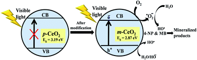
In view of the above mentioned problems, an electrochemically active biofilm (EAB) has been employed on solid surfaces, which has shown potential in bioenergy and chemical production.18 Generally biofilms formed on solid surfaces by different type of microorganism for their mutual benefits. Electrochemically active biofilms (EABs) generated by electrically active microorganisms have properties that can be used to control the electrochemical reactions in a range of fields, such as bioenergy production, bioremediation and chemical/biological synthesis.18 Recently, through a series of studies, previous studies reported that EABs could be used for band gap narrowing of metal oxides, synthesizing noble metal nanoparticles and metal–semiconductor nanocomposites with higher efficiency than many other synthetic methods.19–26 As part of an ongoing study of EAB, the present study focused on the use of EAB for the modification of p-CeO2. This paper reports a very simple, biogenic and facile method for the modification of p-CeO2 by EAB. The enhancement of the photocatalytic activity due to the presence of defects in m-CeO2 was further confirmed by the degradation of 4-nitrophenol (4-NP) and methylene blue (MB) in an aqueous solution under visible light irradiation. A possible charge transfer mechanism was suggested to be involved in the degradation process. The photoelectrochemical result under dark and visible light further support the visible light activity of the m-CeO2 photocatalyst, suggesting the applicability of CeO2 in visible light as a photocatalyst and photoelectrode. m-CeO2 showed high photocatalytic activity compared to p-CeO2. The modification approach reported in this work does not involve the use of hazardous chemicals, capping agents, reducing agents, simple to perform, and has potential for commercialization.
2. Experimental
2.1. Materials
Cerium oxide (nano CeO2) nanostructures and MB were purchased from Sigma-Aldrich. Sodium acetate, sodium sulfate (Na2SO4) and 4-NP were obtained from Duksan Pure Chemicals Co. Ltd South Korea. Ethyl cellulose and α-terpineol were supplied by KANTO Chemical Co., Japan, and fluorine-doped transparent conducting oxide glass (FTO; F-doped SnO2 glass; 7 Ω sq−1) was acquired from Pilkington, USA. Carbon paper (without wet proof, Fuel Cell Earth LLC, USA). All chemicals used in this study were of analytical grade and used as received. All solutions were prepared from deionized water obtained using a PURE ROUP 30 water purification system.
2.2. Methods
X-ray diffraction (XRD, PANalytical, X'pert PRO-MPD, Netherland) was carried out using Cu Kα radiation (λ = 0.15405 nm). The XRD peaks of the crystalline phases were compared with those of standard compounds reported in the JCPDS data file. The size of the pure CeO2 (p-CeO2) and EAB modified CeO2 (m-CeO2) nanostructures were observed by field emission transmission electron microscopy (FE-TEM, Tecnai G2 F20, FEI, USA) with an accelerating voltage of 200 kV combined with energy dispersive spectrometry (EDS) and selected-area electron diffraction (SAED). A UV-VIS-NIR spectrophotometer (VARIAN, Cary 5000, USA) was used to record the diffuse reflectance/absorption spectra (DRS) of the p-CeO2 and m-CeO2 nanostructures in the range of 200–800 nm. The photoluminescence (PL) properties of the p-CeO2 and m-CeO2 were recorded over the range, 200–800 nm, using a Kimon, 1 K, Japan. X-ray photoelectron spectroscopy (XPS, ESCALAB 250) was performed using monochromatized Al Kα X-rays (hν = 1486.6 eV) with a 500 μm spot size. The binding energy of C1s at 284.8 eV was used to calibrate the other binding energies. The XP spectra were fitted using the “Avantage program”. The electron paramagnetic resonance (EPR) measurements were performed using a Bruker EMX system at 20 K. The DC electrical conductivity (σ) was measured using a 4-in-line probe electrical conductivity measuring instrument (Scientific Equipment, India). The photoelectrochemical and photocatalytic experiments were carried out using a 400 W lamp (3 M, λ > 400 nm, USA). Electrochemical impedance spectroscopy (EIS) and linear scan voltammetry (LSV) were performed in a three electrode cell with a 0.2 M Na2SO4 aqueous solution as the electrolyte using a potentiostat (Versa STAT 3, Princeton Research, USA). The working electrodes were prepared using the technique reported elsewhere.21 Briefly, 100 mg of the p-CeO2 and m-CeO2 nanostructures were suspended thoroughly using a conditioning mixer by adding ethyl cellulose as a binder and α-terpineol as the solvent for the paste, and then coated on FTO glass electrode using the doctor-blade method. The p-CeO2 and m-CeO2 nanostructure-coated (FTO) glass substrates were used as the working electrode, Ag/AgCl (saturated with KCl) and Pt gauge were used as the reference and counter electrodes, respectively.
2.3. Development of electrochemically active biofilm
The electrochemically active biofilms (EABs) were developed on plain carbon paper according to previous reports.18–26 In a typical procedure, carbon paper (without wet proof, Fuel Cell Earth LLC) with a size of 2.5 cm × 4.5 cm was dipped into a mineral salt medium containing sodium acetate (1 g L−1) as the substrate and carbon source in a 250 mL bottle. 10 mL of anaerobic sludge (from a biogas plant in Paju, Korea) was added under strict anaerobic conditions by sparging N2 gas for 5 min to remove the environmental oxygen. All media, including the bacterial inoculum, were changed every two days under strict anaerobic conditions. This process was repeated for two weeks to obtain the EAB on the surface of the carbon paper.
2.4. Modification of CeO2 by the electrochemically active biofilm
In a typical modification process (Fig. S1†), 5 mM CeO2 powder was dispersed in 200 mL of distilled water, and 0.2 g sodium acetate (1 g L−1) was added as an electron donor with continuous magnetic stirring for 1 h at room temperature. Subsequently, the as-prepared EAB was hung under anaerobic conditions in the solution with slow magnetic stirring. The color of the solution turned light gray after 72 h. The pH of the above dispersion was checked before and after the reaction and was found to be 7.10 and 7.50 respectively. Subsequently, the dispersion was centrifuged and the product was obtained. The powder was dried and isolated for further characterization.
As a control experiment, one modification process was carried out in the absence of sodium acetate, i.e. in a 5 mM solution of CeO2. The EAB was hung under anaerobic conditions by sparging N2 gas. The other process was performed by adding 0.2 g sodium acetate (1 g L−1) in a 5 mM CeO2 solution in the absence of an EAB under anaerobic conditions by sparging N2 gas. In both cases, no color change was observed, even after 72 h.
2.5. Evaluation of dye degradation
The photocatalytic activities of the p-CeO2 and m-CeO2 nanostructures were evaluated by measuring the degradation of 4-NP and MB under visible light irradiation (λ > 400 nm). In a typical photodecomposition process, 2 mg of each p-CeO2 and m-CeO2 nanostructure photocatalyst was added to two different 20 mL 4-NP (5 mg L−1) and 20 mL MB (10 mg L−1) solutions, and agitated for 30 min in the dark to achieve adsorption–desorption equilibrium. The above suspensions were irradiated with visible light and after a certain time (1 h). Subsequently, 2 mL of the solution was taken and the catalyst was separated from the solution by centrifugation to obtain a clear liquid, of which the UV-vis spectra were measured. The decolorization efficiency of the photocatalyst was determined using the equation reported elsewhere.25
2.6. Photoelectrochemical studies (EIS and LSV)
To examine the photoelectrochemical response of the p-CeO2 and m-CeO2 nanostructures, EIS and LSV experiments were carried out under ambient conditions in the dark and under visible light irradiation in 50 mL of a 0.2 M Na2SO4 aqueous solution at room temperature. For each electrode, EIS was first performed in the dark and later under visible light irradiation (λ > 400 nm) at 0.0 V and with a frequency ranging from 1–104 Hz. The photocurrent response was obtained by LSV under dark and visible light irradiation at a scan rate of 50 mV s−1 over a potential range of −0.7 to 1.0 V.
2.7. DC electrical conductivity measurement
For the DC electrical conductivity measurements, a 0.2 g sample (p-CeO2 and m-CeO2 nanostructures) was pelletized at room temperature using a hydraulic press at 25 kN, applied for 10 min. The DC electrical conductivity (σ) was measured using a 4-in-line probe electrical conductivity measuring instrument, and calculated using the following equation:
σ = [ln![[thin space (1/6-em)]](https://www.rsc.org/images/entities/char_2009.gif) 2(2S/W)]/[2πS(V/I)] 2(2S/W)]/[2πS(V/I)] |
where I, V, W and S are the current (A), voltage (V), thickness of the pellet (cm) and probe spacing (cm), respectively, and σ is the DC electrical conductivity (S cm−1).27
3. Results and discussion
3.1. Proposed modification mechanism
EAB is used as a biogenic tool that provides excess of electrons and protons by biologically decomposing the carbon source (sodium acetate) as shown below:26,28
| CH3COO− + 4H2O + EABs → 9H+ + 8e− + 2HCO3− |
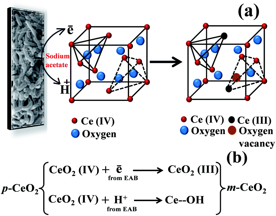
These electrons were used to modify the metal oxide nanostructure.20,21 The advantage of the EAB method to modify the p-CeO2 nanostructure is that it does not require any harmful chemicals, external energy input, capping or reducing agents, and tiresome treatments. The reaction medium for this protocol was water and the entire modification process took place at 30 °C. The product obtained in this synthesis is quite pure and free from impurities as the biofilm was supported on carbon paper. The change in pH from 7.10 to 7.50 is attributed to the dissociation of sodium acetate into CH3COO− and Na+. Formation of CH3COO− ions disturbs the water equilibrium by associating with some H+ and thereby reducing the concentration of H+. This increases the concentration of OH−, hence an increase in pH. The EAB-generated electrons and protons can interact with Ce4+ and surface oxygen, respectively (Fig. 1a). The coordination number of Ce4+ to O2− decreases from eight to seven with the formation of Ce3+ ions in the crystal lattice due to the interactions of electrons with Ce4+.29 The interaction of protons with the surface O atoms can produce –OH, resulting in the formation of Ce–OH linkages (Fig. 1b), which was confirmed by XPS. These interactions are responsible for inducing defects in the CeO2 nanostructure, resulting in visible light absorption by the m-CeO2 nanostructure. In our previous reports the interaction of EAB with ZnO and TiO2 nanostructures was somewhat different because of different types of molecular structures and bonding patterns of ZnO and TiO2.20,21 In case of ZnO, oxygen vacancy was exclusively responsible for the band gap narrowing whereas in case of TiO2, Ti3+ and –OH linkages were responsible for the band gap narrowing.20,21
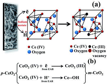 |
| | Fig. 1 (a) Proposed mechanism, and (b) reaction steps involved for modification of the p-CeO2 nanostructure by EAB. | |
3.2. Structural analysis
The structures of the p-CeO2 and m-CeO2 nanostructures were analyzed by XRD. For the m-CeO2 nanostructure (Fig. 2), the XRD peaks correspond to the planes that match well with that of the cubic fluorite CeO2 structure (JCPDS no. 88-2326). Upon modification, the peak positions (2θ) of the m-CeO2 nanostructure shifted toward a lower angle compared to p-CeO2. According to Bragg's law, nλ = 2dsinθ, the d spacing increases with decreasing θ. Therefore, the d spacing of the m-CeO2 nanostructure is slightly larger (3.22 Å) than those of the p-CeO2 nanostructure (3.12 Å). The increasing lattice parameters in m-CeO2 (a = b = c = 5.59 Å) compared to p-CeO2 (a = b = c = 5.41 Å) can be explained in terms of the associated reduction of Ce4+ to Ce3+ and an increase in the number of oxygen vacancies, which leads to lattice expansion.5,30 These were confirmed further by other techniques. This lattice expansion generates residual stress in the matrix, leading to a shift in the peak positions.12 A similar XRD peak shift to a lower angle was observed for the CeO2 nanoparticles with the formation of Ce3+ ions.31
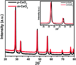 |
| | Fig. 2 XRD patterns of the p-CeO2 and m-CeO2 nanostructures. The inset displays the shifting and broadening of the peaks. | |
3.3. Microstructural study
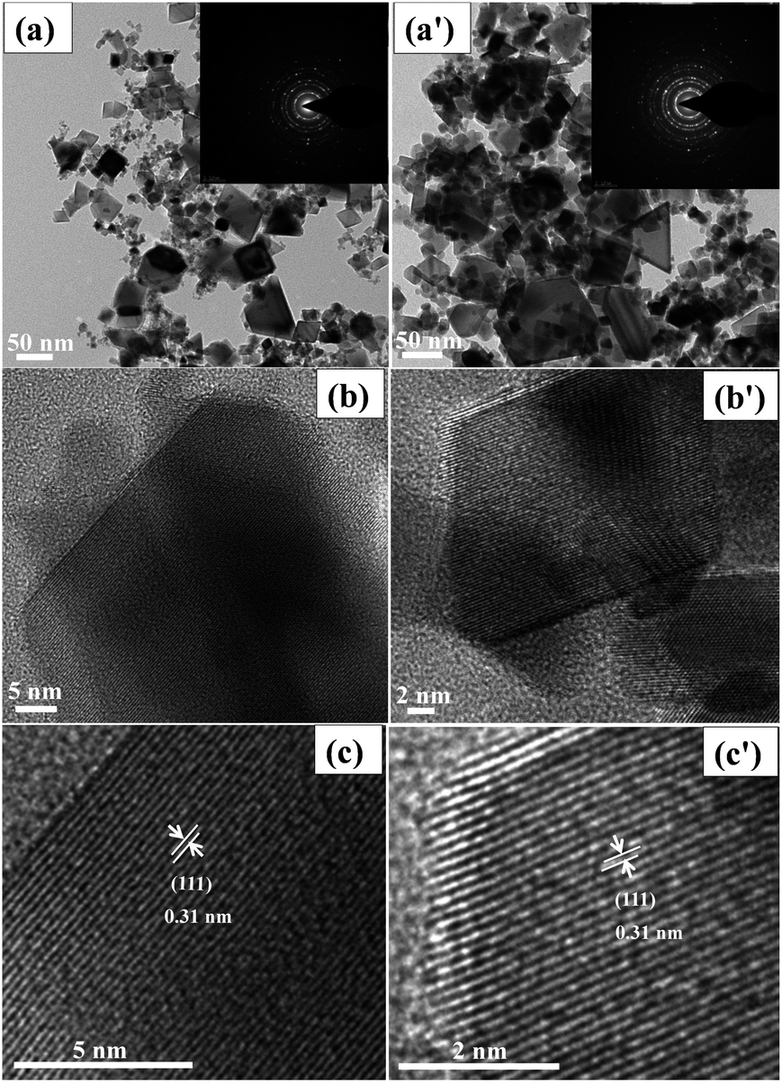
Fig. 3 shows the TEM and HR-TEM images of the p-CeO2 and m-CeO2 nanostructures before the photocatalytic reaction, whereas Fig. S2† shows the TEM and HR-TEM images of the p-CeO2 and m-CeO2 nanostructures after the photocatalytic reaction. Fig. 3a (p-CeO2) and 3a′ (m-CeO2) shows a mixture of spherical and cube shapes of CeO2 nanostructure in the range of 10–50 nm, respectively. The inset in Fig. 3a and a′ corresponds to the SAED pattern, indicating the polycrystalline nature of CeO2 with a fcc structure, which is in good agreement with the XRD patterns. The fringe spacing (Fig. 3c and c′) from the HR-TEM image was 0.31 nm for the p-CeO2 and m-CeO2 nanostructures, which corresponds to the interplanar distance of the (111) plane. The structural compositions of the particles were determined by HAADF-FETEM, as shown in Fig. S3 and S4† for p-CeO2 and m-CeO2, respectively. Fig. S5 and S6† show the EDX spectra of the p-CeO2 and m-CeO2 nanostructures, confirming the modification of p-CeO2 and an absence of other impurities.
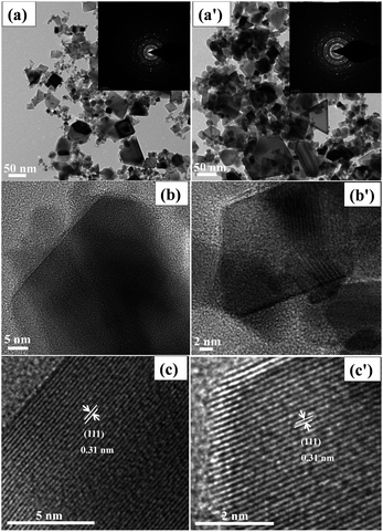 |
| | Fig. 3 TEM and HR-TEM images of the p-CeO2 (a–c) and m-CeO2 (a′–c′) nanostructures before photocatalytic reaction. The insets (a and a′) show the SAED patterns of the p-CeO2 and m-CeO2 nanostructures. | |
3.4. Diffuse absorption/reflectance study
UV-vis diffuse absorption/reflectance spectroscopy was used to evaluate the optical properties of the p-CeO2 and m-CeO2 nanostructures. Fig. 4a and S7† shows the absorption and reflectance spectra of the p-CeO2 and m-CeO2 nanostructures, respectively. The absorption spectra of the p-CeO2 and m-CeO2 nanostructures modified at different time intervals (i.e. 24 h, 48 h and 72 h) are shown in Fig. S8.† The absorption spectra reveal the m-CeO2 nanostructure to have significantly higher absorption in the visible light region. The spectra show that the m-CeO2 nanostructure possesses higher light absorption intensity and a red shifted absorption edge compared to the p-CeO2 nanostructure. Mao et al.,32 in their computational study of nitrogen-doped CeO2 nanoparticles, attributed the absorption (<500 nm) to the additional states caused by doping, whereas the absorption (>500 nm) was associated with defects and oxygen vacancies. The band gap was estimated from a plot of the transformed Kubelka–Munk function versus the energy of absorbed light (Fig. 4b).21,25 The effective optical band gaps of the p-CeO2 and m-CeO2 nanostructures were 3.19 eV and 2.87 eV, respectively, indicating a 0.32 eV difference. This shows that the EAB acted as a band gap modifier.
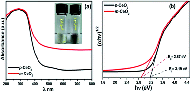 |
| | Fig. 4 (a) UV-vis diffuse absorption spectra of the p-CeO2 and m-CeO2 nanostructures (the inset shows the color of p-CeO2 and m-CeO2 nanostructure), and (b) optical band gap obtained from the plots of (αhν)1/2 versus the photon energy (hν) of the p-CeO2 and m-CeO2 nanostructure. | |
The red shift in the band gap of the m-CeO2 nanostructure is affected by Ce3+ and oxygen defects.12,17,33 Patsalas et al.,34 reported that the red shifting in the band gap is due to an increase in the concentration of Ce3+ on the grain boundaries, and the reduction of the band gap increases with increasing Ce3+ concentration. The band gap narrowing of the m-CeO2 nanostructure was attributed to the high concentration of Ce3+ induced by the defect levels generated in CeO2 because of the interaction with electrons and protons. The higher light absorption intensity of the m-CeO2 nanostructure also suggests that it could enhance the photocatalytic performance, which was confirmed by the photocatalytic degradation of the dyes. These observations suggest that the m-CeO2 nanostructure can be photoexcited to generate more electron–hole pairs under visible light irradiation, which can result in higher photocatalytic performance.
3.5. XPS analysis
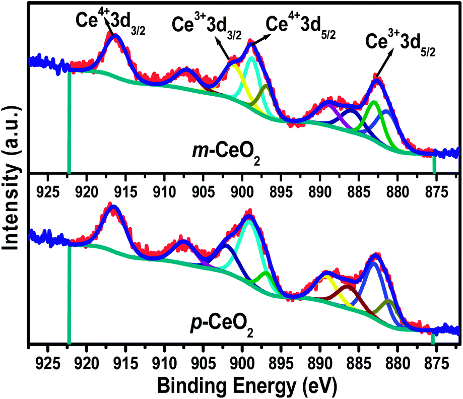
XPS of the p-CeO2 and m-CeO2 nanostructures was performed to examine the chemical composition and valance states of the elements present in the samples. Fig. S9† shows the XP survey spectra of p-CeO2 and m-CeO2, in which all the peaks were assigned to Ce, O and C. No extra peak for any other impurity was observed. The intensity of the C1s peak was higher for p-CeO2 than for the m-CeO2 nanostructures, which was attributed to the removal of surface carbon impurities (Fig. S10†). Fig. 5 shows the Ce 3d core-level fitted spectra with the corresponding deconvoluted Gaussian peaks. The deconvoluted Ce 3d core level spectra reveal the mixed valence states of both Ce3+ and Ce4+ owing to its nonstoichiometric nature and multiple d-splitting, such as 3d3/2 and 3d5/2.5,35 The peak values for 3d3/2 and 3d5/2 were between 895 & 910 eV, and 875 & 890 eV, respectively. The characteristic peaks of the mixed valance, such as Ce4+ 3d3/2 and Ce4+ 3d5/2 were located at binding energies of 916.4 eV and 898.8 eV, respectively, whereas the peaks located at binding energies of 901.1 and 882.7 eV were assigned to Ce3+ 3d3/2 and Ce3+ 3d5/2, respectively.5 The mixed states of CeO2, also determined by additional satellite peaks (which are called ‘shake-up’), were located at 907.2 eV for Ce3+ 3d3/2, and 885.8 and 889.0 eV for Ce3+ 3d5/2, respectively.5 Semiquantitative analysis of each deconvoluted peak area was used to calculate the concentration of Ce3+ in p-CeO2 and m-CeO2. The detailed notation and calculation of Ce 3d spectra of CeO2 can be found elsewhere.5,17,29,35 An analysis of the Ce 3d XP spectra of m-CeO2 showed that the concentration of Ce3+ (0.489) increased compared to p-CeO2 (0.431). The presence of a high concentration of Ce3+ in m-CeO2 confirms the interaction of Ce4+ with the electrons produced by the EAB. During this process, oxygen vacancies can arise to maintain the charge neutrality of the system, which might have some additional contribution to band gap narrowing.36 Passacantando et al.,37 supports the present investigation in that when the concentration of Ce3+ ions becomes higher, their lattice parameters expanded because of the reduced electrostatic force derived from the increased concentration of Ce3+ ions. The correlation between the XPS and XRD data shows that the concentration of Ce3+ ions is proportional to the increase in the lattice parameter.
 |
| | Fig. 5 XPS Ce 3d core level spectra of the p-CeO2 and m-CeO2 nanostructures. | |
Fig. 6 shows the O1s photoemission spectra of the p-CeO2 and m-CeO2 nanostructures. The O1s photoemission spectra also revealed an asymmetric profile and could be deconvoluted into a different symmetrical signal, which shows a different type of oxygen, such as absorbed oxygen, lattice oxygen, surface hydroxyl group and oxygen vacancies.38,35 The low binding energy peak (528.0–530.5 eV) was assigned to lattice oxygen, whereas the high binding energy peak (531.0–532.8 eV) was assigned to oxygen vacancies.39 The peak at 531.50 eV in p-CeO2 shifted to a higher binding energy (531.80 eV), showing the formation of hydroxyl groups on the surface, which might be due to the interaction of protons produced by the EAB. On the other hand, the higher binding energy peak in the O1s spectrum could also be related to the presence of oxygen vacancies.35,36 The reason for the existence of a higher binding energy peak of the O1s spectrum might be the more tightly bonded 1s electron to oxygen in the case of Ce3+ of ceria (O–Ce3+), which interacts with the protons produced by the EAB.36 Despite this, the intensity is also a common way for qualitatively assessing the number of oxygen vacancies in ceria. In the case of m-CeO2, the peak intensity also increases compared to p-CeO2, which might be due to the presence of oxygen vacancies.40
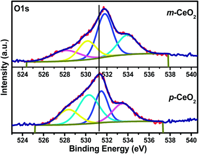 |
| | Fig. 6 XPS O1s core level spectra of the p-CeO2 and m-CeO2 nanostructure. | |
3.6. EPR measurement
Fig. 7a shows the X-band EPR signal of the p-CeO2 and m-CeO2 nanostructures. One signal at 3441 G was observed for p-CeO2 and m-CeO2. This signal at 3441 G has been studied widely and generally attributed to Ce3+ formed in the sample.30,41,42 In this case, the intensity of the Ce3+ signal increases as defects are induced in the m-CeO2 (Fig. 7). This increase in intensity is due to the reduction of Ce4+ ions to Ce3+ after the interaction of CeO2 with electrons produced by EAB, leading to the formation of defects in p-CeO2.41 Fig. S11† shows the g-value spectra of the p-CeO2 and m-CeO2 nanostructures, which indicates the presence of a narrow signal at g = 1.96 and a strong signal at g = 2.00. These signals are typical for Ce3+ in ceria-based materials.42 This also supports the presence of Ce3+ ions and oxygen vacancies in the sample.
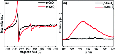 |
| | Fig. 7 (a) X-band EPR spectra, and (b) PL spectra of the p-CeO2 and m-CeO2 nanostructures. | |
3.7. Photoluminescence characteristics
Photoluminescence spectroscopy is normally used to explore the efficiency of charge carrier migration and transfer, and is also helpful for understanding the fate of electron–hole pairs in semiconductor particles.21,25 The band gap narrowing of CeO2 was investigated further by observing the photoluminescence properties. Fig. 7b shows the room-temperature PL spectra of the p-CeO2 and m-CeO2 measured at 325 nm as the excitation source. The broad emission peak from 400 to 500 nm might be responsible for the electronic transition in the narrowed band gap of CeO2. The emission intensity and broadening in m-CeO2 is stronger than that of p-CeO2, indicating the greater abundance of defects in m-CeO2. When there is a higher concentration of Ce3+ states and a corresponding high concentration of oxygen vacancy states, a larger percentage of valence electrons can be excited to the defect state and a larger emission signal will be received.33 The m-CeO2 in this case has strong emission indicating a higher concentration of Ce3+ states compared to p-CeO2. This suggests that m-CeO2 contains more defects (Ce3+ and oxygen vacancy) than the commercial CeO2 nanostructure (p-CeO2), which might be helpful in improving the defect-related properties, such as photocatalytic activity.
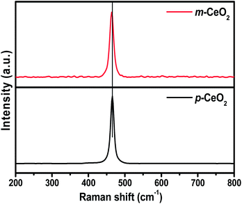
3.8. Raman spectroscopy
Raman spectroscopy is also used as a complementary structural characterization technique because the responses are affected by a range of factors including strain and broadening associated with the size distribution and defects.30,35 Fig. 8 shows the Raman spectra of p-CeO2 and m-CeO2. The Raman spectrum of the m-CeO2 nanostructures was similar to that of p-CeO2, which highlights the purity of CeO2 after modification. Generally, dioxides with afluorite structure have a F2g allowed mode, which is a Raman active mode.12 The F2g reveals the structure of the symmetric breathing pattern of the oxygen atoms around the Ce4+ ions. A peak shift of 1.97 cm−1 and a broadening of the peak was observed in m-CeO2. The peak shift and broadening observed in m-CeO2 was attributed to the change in lattice parameter after the stoichiometric changes and defects (Ce3+ and oxygen vacancy).12,17,30,31 XRD, XPS and DRS confirmed that the stoichiometric changes and defects are responsible for the minor changes in the Raman band.
 |
| | Fig. 8 Raman spectra of the p-CeO2 and m-CeO2 nanostructures. | |
3.9. Visible light photocatalytic activity and its photoexcitation mechanism
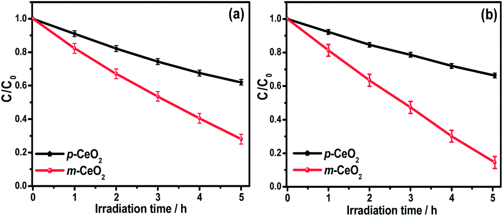
The influence of defects (Ce3+ and oxygen vacancy) on the visible light photocatalytic activity of m-CeO2 nanostructures was examined by measuring the degradation of a colorless aromatic compound (4-NP) and colored dye (MB). The degradation of 4-NP and MB by m-CeO2 was evaluated by the change in the intensity of the absorption peaks. Fig. 9a and b shows plots of degradation (C/C0) versus the irradiation time, where C is the absorption of a 4-NP and MB solution at each time interval of irradiation, and C0 is the absorption of the initial concentration. Fig. 9a and b shows that the m-CeO2 nanostructure has a higher photocatalytic activity than the p-CeO2 nanostructure under similar conditions. Furthermore, the present photocatalytic activity result of the m-CeO2 shows higher photoactivity compared to the EAB modified and commercially available metal oxide nanostructures (Degussa TiO2 and ZnO).20,21
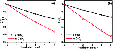 |
| | Fig. 9 Kinetic profile of the photocatalytic degradation of (a) 4-NP, and (b) MB under visible light irradiation in the presence of the p-CeO2 and m-CeO2 nanostructures. | |
Based on the above results, Fig. 10 presents the general mechanism for the photoexcitation and electron transfer properties of the p-CeO2 and m-CeO2 nanostructures for the photocatalytic degradation of 4-NP and MB under visible light irradiation. m-CeO2 showed higher activity than p-CeO2. The UV-vis diffuse absorption spectra (Fig. 4a) and transformed Kubelka–Munk function plots (Fig. 4b) show that the photon absorption in visible light by m-CeO2 increases significantly due to a decrease in band gap. On the other hand, because of the wide band gap of p-CeO2 (3.19 eV), the generation of electron in the conduction bands and holes in the valence bands under visible light is not feasible (Fig. 10). When the band gap of m-CeO2 is reduced significantly to 2.81 eV, electrons from the valance band can migrate easily to the conduction band by absorbing visible light.16 The electrons that accumulate on the surface of m-CeO2 are then scavenged by oxygen molecules dissolved in water to yield highly oxidative species, such as superoxide radical anions and hydroxyl radicals, which are responsible for decomposing and mineralizing 4-NP and MB.21,25 Following are the proposed reactions that occurred during the degradation of pollutants in the presence of m-CeO2.20,25,43,44
| m-CeO2 + hν (visible light) → e− + h+ |
| ˙OH + pollutants → degradation of pollutants |
 |
| | Fig. 10 Proposed mechanism for the photodegradation of 4-NP and MB by the p-CeO2 and m-CeO2 nanostructures. | |
Generally, photocatalytic processes comprises the generation of electron–hole pairs through the absorption of suitable photon energy, separation of the photogenerated charge carriers, and surface redox reactions, which are responsible for the production of highly active oxidation species. On the other hand, expansion in the visible light absorption region alone cannot ensure high photocatalytic activity because the separations of the photogenerated electron–hole pairs and their migration to the surface reaction sites also plays an important role in determining the photocatalytic performance.1,2,5 Upon the irradiation of visible light, the vacancy states might also promote visible-light absorption and the generation of photoexcited electron–hole pairs over the surface of m-CeO2. The superior visible light photocatalytic activity of m-CeO2 can be explained based on the defects (Ce3+ and oxygen vacancy) and band gap narrowing. The transformation of Ce4+ to Ce3+ and oxygen vacancies might have played a key role in increasing the photocatalytic activities of m-CeO2.
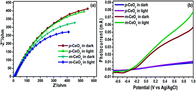
3.10. Photoelectrochemical study
EIS was performed under dark and visible light irradiation to supply further evidence to support the enhanced visible light photocatalytic activity of m-CeO2 (Fig. 11a). The semicircle in the Nyquist plot is the expected response of the simple circuit. EIS Nyquist plots were also employed to examine the charge transfer resistance and separation efficiency between the photogenerated electrons and holes.21,45,46 The semicircular arcs in the EIS spectra were assigned to the contribution from the charge transfer resistance (Rct) and constant phase element (CPE) at the photocatalyst/electrolyte interface. Fig. 11a shows that the arc radius in the EIS of m-CeO2 under visible light irradiation is smaller than that of p-CeO2. This suggests that m-CeO2 has a lower resistance and effective separation of photogenerated electron–hole pairs than that of p-CeO2. Moreover, the m-CeO2 exhibits more effective separation of the photogenerated electrons–holes pairs and faster interfacial charge transfer.21 EIS showed that the photo active sample (m-CeO2) with a lower charge transfer resistance has a higher photocatalytic activity for dye degradation.
 |
| | Fig. 11 (a) Nyquist plots of the p-CeO2 and m-CeO2 nanostructures photoelectrodes under dark and visible light irradiation, and (b) linear scan voltammograms obtained for p-CeO2 and m-CeO2 nanostructures photoelectrodes under dark and visible light irradiation. | |
3.11. Photocurrent measurement
To examine the possible mechanisms for the enhanced photoreactivity, the LSV for the p-CeO2 and m-CeO2 nanostructures (Fig. 11b) were measured in the dark and visible light illumination.47 The improvement in the photocurrent response of m-CeO2 was attributed to the increase in light absorption ability due to defects that create a mid-gap density of states that help narrow the band gap of CeO2. Owing to the sufficiently narrow band gap of m-CeO2, the valence electrons can be excited to the conduction band state by absorbing visible light. The photoelectrochemical activity is determined by both the light-harvesting capacity and the separation of electron–hole pairs.47–50 The electron–hole pairs are generated by absorbing the incident photons with energies greater than Eg, and recombination might occur unless they are not separated quickly. Generally, a high photocurrent suggests that the sample holds strong ability for generating and transferring the photoexcited charge carrier under irradiation.17 m-CeO2 has a higher photocurrent than p-CeO2 under the same conditions, suggesting that m-CeO2 exhibits stronger ability in the separation of electron–hole pairs than p-CeO2, as shown by PL analysis. The significant improvement in the photocurrent of m-CeO2 suggests that it may be excited easily by visible light, and produce more photoinduced carriers, thereby possessing higher visible light photocatalytic activity.17 In addition, the EIS Nyquist plot (under visible light) also showed that the efficiency of charge separation of m-CeO2 is much higher than that of p-CeO2, indicating that m-CeO2 has higher visible photocatalytic activity.
3.12. Defect-induced DC electrical conductivity
The defects created in m-CeO2 by EAB and their effects on the electrical properties of m-CeO2 were studied to understand the performance in terms of applications. Nano CeO2, like most metal oxide nanostructures, exhibits conductivity in the semiconducting range. The poor electrical conductivity limits the application of CeO2 in electrical devices.4 Many studies have reported that metal doping increases the electrical conductivity. Q. Li,51 in their Mo-doped CeO2-materials, reported an increase in the electrical conductivity with increasing the Mo content. Similar results were also reported by L. Chen et al.,52 and Z. Khakpour et al.,53 in their Gd-doped CeO2 thin films and Sm-doped CeO2, respectively. The preferential defect (oxygen vacancy) formation at the grain boundary sites is indicated as the major reason for the increase in electrical conductivity.54 In the present case, the EAB induced defects (oxygen vacancy) in CeO2, which is advantageous because of its greener route compared to the other methods reported. The DC electrical conductivity of p-CeO2, as measured using the 4-in-line probe device, was found to be 3.142 × 10⁻⁶ S cm−1, whereas that of m-CeO2 was 3.142 × 10⁻³ S cm−1, which is 1000 times higher than p-CeO2. On the other hand, the measured DC electrical conductivity of the m-CeO2 was too high to be attributed only to the defects created by EAB. Therefore, an EAB can be an effective tool for inducing defects, and increasing the electrical conductivity of semiconducting metal oxide materials.
3.13. Stability and reusability of the m-CeO2
The reusability of m-CeO2 was tested by centrifuging the catalyst from the dye solution, later washing with DI water and drying in an air oven at 100 °C. The reused catalyst showed a similar response to that of the fresh catalyst, highlighting the stability and reusability of m-CeO2 nanostructures.
4. Conclusions
A pure CeO2 nanostructure was modified by EAB for visible light applications. XRD, DRS, XPS, PL, Raman, EPR, EIS, visible light photocatalysis and photocurrent (LSV) showed that defect-induced properties developed in pure CeO2 after the interaction with electrons and protons produced by EAB. A mechanism for modifying the p-CeO2 nanostructure was proposed. The absorption spectrum of m-CeO2 exhibited a red shift and remarkably enhanced PL intensity with respect to the p-CeO2 nanostructure due to an increase in the number of defects in the m-CeO2 nanostructure. m-CeO2 also showed significantly higher photocatalytic activity towards 4-NP and MB degradation under visible light irradiation, which was attributed to an increase in the number of defects. These enhanced optical properties, visible light photocatalysis and resulting high photoelectrochemical performance of the m-CeO2 nanostructures provide an interesting novel approach that can advance the field of photocatalysis. The DC electrical conductivity of m-CeO2 was higher than that of p-CeO2 under ambient conditions possibly due to defect formation. These results suggest that Ce3+ and oxygen vacancies can be produced in the p-CeO2 nanostructure by a biogenic method. This novel concept to engineer the band gap of CeO2 is expected to have a significant impact in a range of applications.
Acknowledgements
This study was supported by Basic Science Research Program through the National Research Foundation of Korea (NRF) funded by the Ministry of Education, Science and Technology (Grant no.: 2012R1A1A4A01005951).
References
- C. Sun, H. Li and L. Chena, Energy Environ. Sci., 2012, 5, 8475–8505 CAS.
- Y. Wang, Q. Wang, X. Zhan, F. Wang, M. Safdar and J. He, Nanoscale, 2013, 5, 8326–8339 RSC.
- J. S. Lee, K. H. You and C. B. Park, Adv. Mater., 2012, 24, 1084–1088 CrossRef CAS PubMed.
- C. T. Campbell and C. H. F. Peden, Science, 2005, 309, 713–714 CrossRef CAS PubMed.
- H. Li, G. Wang, F. Zhang, Y. Cai, Y. Wang and I. Djerdj, RSC Adv., 2012, 2, 12413–12423 RSC.
- B. Murugan and A. V. Ramaswamy, J. Am. Chem. Soc., 2007, 129, 3062–3063 CrossRef CAS PubMed.
- H. Y. Yahiro, K. Baba, H. Eguchi and J. Arai, J. Electrochem. Soc., 1988, 135, 2077–2080 CrossRef CAS PubMed.
- N. Izu, W. Shin, N. Murayama and S. Kanzaki, Sens. Actuators, B, 2002, 87, 95–98 CrossRef CAS.
- H. Gu and M. D. Soucek, Chem. Mater., 2007, 19, 1103–1108 CrossRef CAS.
- S. Tsunekawa, T. Fukuda and A. Kasuya, J. Appl. Phys., 2000, 87, 1318–1321 CrossRef CAS PubMed.
- D. Channeia, B. Inceesungvorn, N. Wetchakun, S. Phanichphant, A. Nakaruk, P. Koshy and C. C. Sorrell, Ceram. Int., 2013, 39, 3129–3134 CrossRef PubMed.
- B. Choudhury and A. Choudhury, Mater. Chem. Phys., 2012, 131, 666–671 CrossRef CAS PubMed.
- Z. Wu, M. Li, J. Howe, H. M. Meyer and S. H. Overbury, Langmuir, 2010, 26, 16595–16606 CrossRef CAS PubMed.
- H. Hojo, T. Mizoguchi, H. Ohta, S. D. Findlay, N. Shibata, T. Yamamoto and Y. Ikuhara, Nano Lett., 2010, 10, 4668–4672 CrossRef CAS PubMed.
- X. Liu, K. Zhou, L. Wang, B. Wang and Y. Li, J. Am. Chem. Soc., 2009, 131, 3140–3141 CrossRef CAS PubMed.
- J. W. Ko, J. H. Kim and C. B. Park, J. Mater. Chem. A, 2013, 1, 241–245 CAS.
- X. Lu, D. Zheng, P. Zhang, C. Liang, P. Liu and Y. Tong, Chem. Commun., 2010, 46, 7721–7723 RSC.
- S. Kalathil, M. M. Khan, J. Lee and M. H. Cho, Biotechnol. Adv., 2013, 31, 915–924 CrossRef CAS PubMed.
- M. M. Khan, S. Kalathil, J. Lee and M. H. Cho, Bull. Korean Chem. Soc., 2012, 33, 2592–2596 CrossRef CAS.
- S. Kalathil, M. M. Khan, S. A. Ansari, J. Lee and M. H. Cho, Nanoscale, 2013, 5, 6323–6326 RSC.
- S. A. Ansari, M. M. Khan, S. Kalathil, A. Nisar, J. Lee and M. H. Cho, Nanoscale, 2013, 5, 9238–9246 RSC.
- S. Kalathil, J. Lee and M. H. Cho, Green Chem., 2011, 13, 1482–1485 RSC.
- M. M. Khan, S. A. Ansari, J. Lee and M. H. Cho, Mater. Sci. Eng., C, 2013, 33, 4692–4699 CrossRef CAS PubMed.
- M. M. Khan, J. Lee and M. H. Cho, Int. J. Hydrogen Energy, 2013, 38, 5243–5250 CrossRef CAS PubMed.
- M. M. Khan, S. A. Ansari, J. Lee and M. H. Cho, Nanoscale, 2013, 5, 4427–4435 RSC.
- M. M. Khan, S. A. Ansari, J. H. Lee, J. Lee and M. H. Cho, ACS Sustainable Chem. Eng., 2014, 2, 423–432 CrossRef CAS.
- M. O. Ansari and M. Faiz, J. Appl. Polym. Sci., 2012, 124, 4433–4442 CAS.
- B. E. Logan, D. Call, S. Cheng, H. V. M. Hamelers, T. H. J. A. Sleutels, A. W. Jeremiasse and R. A. Rozendal, Environ. Sci. Technol., 2008, 42, 8630–8640 CrossRef CAS.
- D. Sameer, P. Swanand, V. N. T. K. Satyanarayana and S. Seal, Appl. Phys. Lett., 2005, 87, 133113–133116 CrossRef PubMed.
- V. D. Araújo, W. Avansi, H. B. de Carvalho, M. L. Moreira, E. Longo, C. Ribeiroand and M. I. B. Bernardi, CrystEngComm, 2012, 14, 1150–1154 RSC.
- F. Zhang, S. W. Chan, J. E. Spanier, E. Apak, Q. Jin, R. D. Robinson and I. P. Herman, Appl. Phys. Lett., 2002, 80, 127–130 CrossRef CAS PubMed.
- C. J. Mao, Y. X. Zhao, X. F. Qiu, J. J. Zhu and C. Burda, Phys. Chem. Chem. Phys., 2008, 10, 5633–5638 RSC.
- N. Shehata, K. Meehan, M. Hudait and N. Jain, J. Nanopart. Res., 2012, 14, 1173–1183 CrossRef.
- P. Patsalas, S. Logothetidis, L. Sygellou and S. Kennou, Phys. Rev. B: Condens. Matter Mater. Phys., 2003, 68, 035104–035113 CrossRef.
- F. Meng, L. Wang and J. Cui, J. Alloys Compd., 2013, 556, 102–108 CrossRef CAS PubMed.
- L. R. Shah, B. Ali, H. Zhu, W. G. Wang, Y. Q. Song, H. W. Zhang, S. I. Shah and J. Q. Xiao, J. Phys.: Condens. Matter, 2009, 21, 486004–486009 CrossRef PubMed.
- M. Passacantando and S. Santucci, J. Nanopart. Res., 2013, 15(1785), 1–6 Search PubMed.
- L. Torrente-Murciano, A. Gilbank, B. Puertolas, T. Garcia, B. Solsona and D. Chadwick, Appl. Catal., B, 2013, 132–133, 116–122 CrossRef CAS PubMed.
- A. Galtayries, R. Sporken, J. Riga, G. Blanchard and R. Caudano, J. Electron Spectrosc. Relat. Phenom., 1998, 88, 951–956 CrossRef.
- M. F. Montemora, R. Pinto and M. G. S. Ferreira, Electrochim. Acta, 2009, 54, 5179–5189 CrossRef PubMed.
- A. Aboukaïs, S. Aouad, H. El-Ayadi, M. Skaf, M. Labaki, R. Cousin and E. Abi-Aad, Mater. Chem. Phys., 2012, 137, 34–41 CrossRef PubMed.
- L. Wang, Q. Luan, D. Yang, X. Yao and K. Zhou, RSC Adv., 2013, 3, 6339–6342 RSC.
- H. Chen, C. E. Nanayakkara and V. H. Grassian, Chem. Rev., 2012, 112, 5919–5948 CrossRef CAS PubMed.
- M. Pelaez, N. T. Nolan, S. C. Pillai, M. K. Seery, P. Falaras, A. G. Kontos, P. S. M. Dunlop, J. W. J. Hamilton, J. A. Byrne and K. O'Shea, Appl. Catal., B, 2012, 125, 331–349 CrossRef CAS PubMed.
- S. A. Ansari, M. M. Khan, J. Lee and M. H. Cho, J. Ind. Eng. Chem., 2013 DOI:10.1016/j.jiec.2013.08.006.
- X. Bai, L. Wang, R. Zong, Y. Lv, Y. Sun and Y. Zhu, Langmuir, 2013, 29, 3097–3105 CrossRef CAS PubMed.
- J. Gan, X. Lu, J. Wu, S. Xie, T. Zhai, M. Yu, Z. Zhang, Y. Mao, S. C. Wang, Y. Shen and Y. Tong, Sci. Rep., 2013, 3, 1021–1028 Search PubMed.
- W. Li, M. Li, S. Xie, T. Zhai, M. Yu, C. Liang, X. Ouyang, X. Lu, H. Li and Y. Tong, CrystEngComm, 2013, 15, 4212–4216 RSC.
- M. M. Khan, S. A. Ansari, D. Pradhan, M. Omaish, D. H. Han, J. Lee and M. H. Cho, J. Mater. Chem. A, 2014, 2, 637–644 CAS.
- S. A. Ansari, M. M. Khan, M. Omaish, J. Lee and M. H. Cho, J. Phys. Chem. C, 2013, 117, 27023–27030 CAS.
- Q. Li and V. Thangadurai, Fuel Cells, 2009, 9, 684–698 CrossRef CAS PubMed.
- L. Chen, C. L. Chen, D. X. Huang, Y. Lin, X. Chen and A. J. Jacobson, Solid State Ionics, 2004, 175, 103–106 CrossRef CAS PubMed.
- Z. Khakpour, A. A. Yuzbashi, A. Maghsodipour and K. Ahmadi, Solid State Ionics, 2012, 227, 80–85 CrossRef CAS PubMed.
- N. Li, K. Du, G. Liu, Y. Xie, G. Zhou, J. Zhu, F. Li and H.-M. Cheng, J. Mater. Chem. A, 2013, 1, 1536–1539 CAS.
Footnote |
| † Electronic supplementary information (ESI) available: Schematic representation of modification process, HAADF FE-TEM images, EDX, DRS spectra, XPS survey, C1s and EPR spectra of p-CeO2 and m-CeO2 nanostructures. See DOI: 10.1039/c4ra00861h |
|
| This journal is © The Royal Society of Chemistry 2014 |
Click here to see how this site uses Cookies. View our privacy policy here.