 Open Access Article
Creative Commons Attribution 3.0 Unported Licence
Reduced ionic conductivity in biaxially compressed ceria
Weida
Shen
*a,
Jun
Jiang
b and
Joshua L.
Hertz
ab
aDepartment of Mechanical Engineering, University of Delaware, 126 Spencer Laboratory, Newark, DE 19716, USA. E-mail: weida@ udel.edu; Fax: +1 302 831 3619; Tel: +1 302 831 8452
bDepartment of Materials Science and Engineering, University of Delaware, 201 DuPont Hall, Newark, DE 19716, USA
First published on 7th May 2014
Abstract
Interfacial lattice mismatch strain has been controversially suggested as a means to alter ionic conductivity in solid ion conductors. Here, thin film multilayers composed of yttria-doped ceria (YDC) and Ce1−xZrxO2 (CZO) allow systematic quantification of the effect of biaxial compressive strain on oxygen ion conductivity in ceria. Since the lattice parameter of CZO is highly dependent on the Ce/Zr atomic ratio, its use enables precise control of the strain magnitude in neighboring lattice planes of YDC. Three series of multilayers were fabricated using Ce0.55Zr0.45O2 (CZO45), Ce0.70Zr0.30O2 (CZO30), and CeO2, with an interfacial lattice mismatch of −2.2%, −1.5%, and near-zero, respectively. The compressive strain in the YDC layers caused fairly drastic reductions in the ionic conductivity. Each 1% increase in compressive strain in the YDC yields a 1.6-fold reduction in interfacial conductivity at 650 °C and a 3-fold reduction at 450 °C. Other interfacial effects, however, were also found to have significant impact on the ionic conduction.
1. Introduction
Decreasing the operating temperature of solid oxide fuel cells (SOFCs) to below ≈600 °C is crucial to wider commercialization of this power technology in both stationary and portable power applications.1–3 For this to happen, the low temperature oxygen ion conductivity of electrolyte materials, such as yttria-stabilized zirconia (YSZ), must be increased. In recent studies, nanostructured multilayers or heterostructures using different oxygen-ion conducting oxides have become of great interest.4–7 The driving force behind this trend is the notion that the interfaces between two oxides may have significantly altered—ideally improved—ionic transport behavior.Multilayers composed of undoped BaF2 and CaF2 showed great potential in using nanostructured heterostructures to improve ionic conductivity.8 F− ion redistribution in space charge regions adjacent to the interfaces was used to explain the enhancement of F− ion conductivity as the linear density of interfaces increased.9,10 For systems involving oxygen ion conductors, past studies have typically studied multilayers containing doped conductors (e.g., ZrO2 and/or CeO2).11–16 The relatively high dopant concentrations make the resulting space charge regions inconsequently thin with thickness of only ≈1 Å.12 Space charge effects on oxygen ion conduction—the creation of new defects—in these multilayered films can thus likely be neglected.
Instead, the mobility of existing defects is presumed to be altered by interfacial strains caused by the lattice mismatch between two adjacent layers. Korte et al. and Schichtel et al. have investigated multilayers of YSZ with various insulating rare earth oxides (e.g., Y2O3, Sc2O3, and Lu2O3).12,13,17,18 Tensile strain (decreased pressure) induced in the YSZ layers increased the ionic conductivity, while compressive strain (increased pressure) decreased it. These experimental results, however, have proven difficult to repeat. Garcia-Barriocanal et al. claimed an eight order of magnitude enhancement of conductivity in tensile-strained YSZ/SrTiO3 multilayers,19 though the interpretation of the results has been the subject of debate.20,21 A recent study carried out by Pergolesi et al. found that multilayers of YSZ and CeO2, where a lattice mismatch of ≈5% ostensibly creates tensile strain in the YSZ near the interfaces, had no effect on oxygen ion transport.15
In this work, multilayers composed of Ce0.90Y0.10O2−δ (YDC) and Ce1−xZrxO2 (CZO) were prepared in order to quantify the effect of biaxial compressive strain on oxygen ion conduction. A unique fabrication method that allows creation of thin films with composition controlled at the single nanometer level within wide solid solution compositional spaces was used. This technique enables continuously variable compressive strains to be induced in the YDC layers by controlling the Ce/Zr atomic ratio—and thereby the lattice parameter—in the CZO layers. Another key benefit of using CZO instead of rare earth or other oxides is that both component films in the multilayer are cubic fluorite structure, increasing the likelihood of obtaining coherent interfaces. CZO has a cubic structure at low Zr concentrations of x < 0.5, but can be tetragonal or monoclinic at higher concentrations.22,23 Only cubic CZO is employed in this work.
2. Experimental
Thin films were fabricated by reactive sputtering from single element targets of Ce, Zr, and Y (ACI Alloys, San Jose, CA) in a multi-target, magnetron sputtering machine (PVD Products, Wilmington, MA). A working gas with an oxygen/argon ratio of 1![[thin space (1/6-em)]](https://www.rsc.org/images/entities/char_2009.gif) :
:![[thin space (1/6-em)]](https://www.rsc.org/images/entities/char_2009.gif) 9 was introduced into the sputtering chamber for deposition of oxidized films. The total flow rate was maintained at 20 sccm with a working pressure of 1.33 Pa (10 mTorr). Single crystal Al2O3 with (0001) orientation (MTI Corporation, Richmond, CA) was used as substrates (10 mm × 10 mm × 0.5 mm). During the sputtering process, the substrates were electrically grounded, rotated, and heated to 650 °C. Different layers in a multilayered film were sputtered sequentially using a computerized program that controlled the power applied to each target and/or the toggling of desired target shutters. Further details on the creation and verification of the multilayered film compositions can be found in previous reports.24,25
9 was introduced into the sputtering chamber for deposition of oxidized films. The total flow rate was maintained at 20 sccm with a working pressure of 1.33 Pa (10 mTorr). Single crystal Al2O3 with (0001) orientation (MTI Corporation, Richmond, CA) was used as substrates (10 mm × 10 mm × 0.5 mm). During the sputtering process, the substrates were electrically grounded, rotated, and heated to 650 °C. Different layers in a multilayered film were sputtered sequentially using a computerized program that controlled the power applied to each target and/or the toggling of desired target shutters. Further details on the creation and verification of the multilayered film compositions can be found in previous reports.24,25
θ − 2θ X-ray diffraction (XRD) measurements were performed to determine the orientations of the films using a Philips X'Pert diffractometer with Cu Kα radiation. Lift-off photolithography was employed to fabricate platinum interdigitated electrodes on the surface of the films. The electrodes were laterally spaced by 100 μm with a total perimeter length of about 115 mm. Impedance spectra between 1 Hz and 3 MHz with a signal voltage of 10 mV were measured with a Novocontrol Alpha-A analyzer after heating the samples in air to 650 °C. Though no evidence suggests partial reduction of the films after deposition, if the films were incompletely oxidized, re-oxidation is expected to occur quickly under these conditions. Further, the conductivity was calculated from impedance values that were stable upon repeatedly cycling the temperature up to 650 °C and then measuring every 50 °C as the temperature decreased. This indicates that the material was fully, stably oxidized during the impedance measurements.
At 650 °C, the electrical conductivity of CZO is in the order of 10−4 S cm−1.26 Since the lateral conduction length (i.e., the electrode spacing) of the samples (≈100 μm) was much bigger than the total thickness of CZO (≈50 nm), the current quickly penetrates under the electrode to the entire thickness of the multilayer. The current does not remain confined to just the top layer of YDC.
3. Results and discussion
Three different types of multilayers composed of Ce0.90Y0.10O2−δ (YDC) with CeO2, with Ce0.70Zr0.30O2 (CZO30), or with Ce0.55Zr0.45O2 (CZO45), were prepared. Since the atomic radius of Y3+ is relatively similar to that of Ce4+,27 the lattice parameter of YDC with low concentration of Y-dopants is nearly the same as that of pure CeO2 (aCeO2 ≈ 5.41 Å). A value of ≈5.408 Å was estimated by Hayashi et al. for Ce0.90Y0.10O2−δ using molecular dynamics calculations.28 The interfacial lattice mismatch between YDC and CeO2 can thus likely be neglected. The lattice parameter of CZO is linearly dependent on the Zr content. By Vegard's law, the lattice parameters of CZO45 and CZO30 solid solutions can be estimated as 5.29 Å and 5.33 Å, respectively. Thus, the interfacial lattice mismatch is approximately −2.2% for YDC/CZO45 and −1.5% for YDC/CZO30 interfaces. The negative sign indicates an in-plane compressive strain is expected to be induced in the YDC layers.Prior work by the authors confirmed nearly epitaxial growth of YSZ but not ceria on Al2O3 substrates.29 In order to obtain epitaxial multilayered films in this work, a 5 nm-thick YSZ buffer layer was placed on the Al2O3 substrates. The layered structure of the multilayers can be described as
| Al2O3–YSZ (5 nm-thick)–CZO–(YDC–CZO) × N |
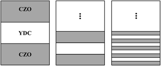 | ||
| Fig. 1 Schematic diagram of the multilayered structures composed of alternating layers of YDC and CZO. | ||
Fig. 2(a) shows the θ − 2θ XRD patterns of YDC/CZO45 multilayers. All of the multilayers display only (111) texture. For N = 1, two separate peaks corresponding to the reflections from (111) planes of YDC and CZO45 were identified. The (111) diffraction peak of YDC is located at lower 2θ is because of its larger lattice parameter compared to that of CZO45. As the number of bilayers is increased, the two peaks of (111) YDC and (111) CZO45 begin to overlap, resulting in the superlattice patterns for N = 3 and N = 7. The superlattice patterns are composed of an average structure peak SL0 surrounded by two first-order satellite peaks, SL−1 and SL+1. For N = 10, where the YDC and CZO layers are 5 nm thick, the diffraction pattern consists almost entirely of a single peak at θ = 28.49°, indicating that the film has largely adopted a single out-of-plane lattice parameter of 5.426 Å. Thus, the lattice mismatch in this structure has effectively biaxially compressed the YDC (and dilated the CZO). The XRD pattern of YDC/CZO30, as shown in Fig. 2(b), also exhibits superlattice effects subsiding to a single peak when the number of bilayers is increased. Fig. 2(c) shows the XRD patterns of YDC/CeO2 multilayers. Due to the similarity of the lattice parameters of YDC and CeO2, it is hard to distinguish any peak separation of the (111) diffraction planes.
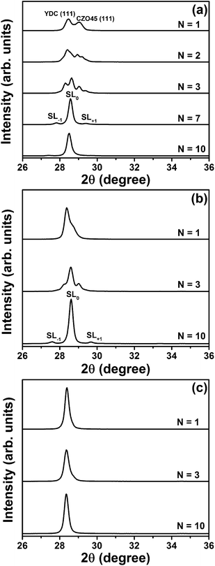 | ||
| Fig. 2 θ − 2θ XRD patterns of multilayers composed of (a) YDC with CZO45, (b) YDC with CZO30, and (c) YDC with CeO2 deposited on Al2O3 (0001) substrates. N indicates the number of YDC/CZO bilayers. | ||
The appearance of sharp, well-defined satellite peaks indicates the formation of high-quality interfaces between the adjacent layers. The locations of the satellite peaks in XRD patterns can be used to calculate the bilayer thickness according to
 | (1) |
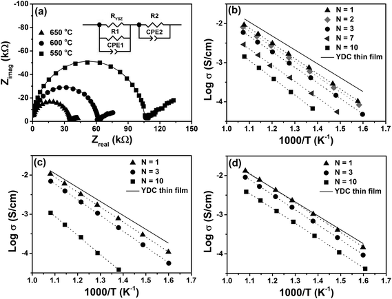
The impedance spectra of all the multilayers exhibit two main features composed of two semicircles located at high and low frequencies, as shown in Fig. 3(a). The equivalent circuit inset in the figure was used to fit the corresponding impedance spectrum at each temperature. The equivalent capacitance of the constant phase element for the high frequency semicircle, CPE1, was of order 10−11 F, while a much larger equivalent capacitance value of >10−7 F was obtained for that of the low frequency semicircle, CPE2. Such large difference in capacitance allowed clear determination that the high frequency semicircle is due to the ionic conduction through the electrolyte, while the low frequency semicircle is due to electrode polarization. The electrical resistance of the 5 nm-thick YSZ buffer layer, RYSZ, was calculated based on the electrode geometry and the conductivity value obtained from ref. 29 for a 100 nm thick YSZ film with the same dopant concentration. The value of RYSZ was always at least one order of magnitude larger than that of R1. Resistance R1, therefore, represents the electrical resistance of the electrolyte eliminating the small contribution from the YSZ buffer layer.
The electrical conductivity of pure CeO2 at 650 °C is normally of order 10−3 S cm−1,30 which is at least one order of magnitude less compared to that of YDC thin film. By adding ZrO2 into CeO2 to form CZO solid solution, the conductivity is further decreased due to reduced vacancy mobility.31 The contribution from the parallel CZO layers to the total electrical conductivity of the multilayers discussed here is negligible, with a parallel resistance that was, like the YSZ buffer layers, always at least one order of magnitude larger than that of the YDC layers. The total electrical conductivity of the multilayers was calculated based on the resistance R1 and the total thickness of the YDC layers.
Fig. 3(b) shows the Arrhenius plots of the electrical conductivity measured for YDC/CZO45 multilayers in air. The conductivity of a single-layer YDC thin film (195 nm-thick) is also included for comparison. The out-of-plane lattice parameter for this single-layer YDC thin film was calculated to be about 5.409 Å based on the (111) XRD diffraction peak. This value is similar to what was found by Hayashi et al. for bulk YDC with the same Y-dopant concentration.28 The YDC single-layer film is fully relaxed due to the relatively large thickness. Any possible strain effect caused by the lattice mismatch with the substrate can be safely excluded. From Fig. 3(b), it can be seen that the electrical conductivity of YDC/CZO45 multilayers monotonically decreased by almost one order of magnitude as the number of bilayers was increased from N = 1 to 10. At the same time, the activation energy increased from 0.84 eV to 0.95 eV.
Fig. 3(c) show similar trends of reduced electrical conductivity with increasing number of bilayers for the YDC/CZO30. For both N = 1 and 3, the electrical conductivity of YDC/CZO30 is larger than that of YDC/CZO45 due to the smaller lattice mismatch. For N = 10, with individual layer thickness of ≈5 nm, the conductivity of the YDC/CZO30 is slightly smaller compared to that of YDC/CZO45. This may be due to the experimental variability. In general, the conductivity of the YDC decreases as the interfacial density and/or the lattice mismatch increase. The electrical conductivity of the YDC/CeO2 multilayers, as shown in Fig. 3(d), decreases as the number of bilayers increases, despite near-zero strain in the multilayers. The mechanism of this effect is either interfacial roughness or substrate-related effects. At N = 10, the layers are only 5 nm thick, and thus even 1 nm interfacial roughness could lead to significant current constriction at the thinnest areas. Alternatively, this slight decrease in conductivity may be due to the N = 3 and N = 10 multilayers placing the first YDC layer in closer proximity to the YSZ buffer layer and substrate beneath.
In order to better understand the conduction behavior of the multilayers with different lattice mismatch, the conduction paths through the YDC layers can be deconvoluted into two independent, parallel parts.32 The first part is conduction through the YDC volume or bulk regions in which the oxygen ion conduction is assumed to be unaffected by the interfacial lattice strain. The second part is the conduction through the interfacial YDC regions near the CZO. The volume and interfacial conductivities each contribute to the total conductance, as derived in ref. 32:
 | (2) |
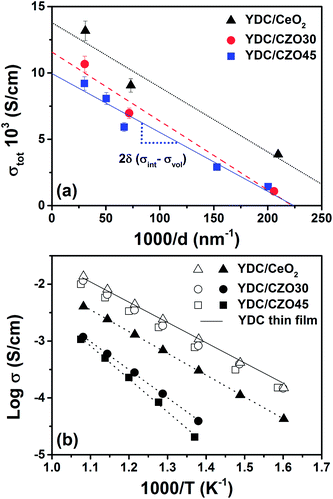
Fig. 4(a) shows the total conductivities at 650 °C of all of the multilayer samples as a function of the reciprocal thickness of the YDC layers. A linear fit of the data allows calculation of the volume and interfacial conductivities of the YDC layers. The latter of these, σint, can be estimated from the slope if the thickness of the strained interfacial regions can be estimated. Since the conductivity of each type of multilayer continues to decrease even as the individual layer thickness becomes 5 nm, the thickness of the strained interfacial regions is ≤2.5 nm. We assume here that the thickness of the strained interfacial regions was 2.5 nm, but it may be slightly smaller.
Fig. 4(b) gives an Arrhenius plot of the calculated volume and interfacial conductivities of the three different types of multilayers. The volume conductivities are all very similar to that of the YDC single-layer film. This is expected, since the volume regions of the YDC layers in these multilayers were assumed not to be affected by the interfacial strain. The interfacial conductivity for the YDC/CeO2 multilayers is about half an order of magnitude less than that of the volume conductivity, while that of the YDC/CZO30 and YDC/CZO45 multilayers is much smaller. The interfacial conductivity of the YDC/CZO30 multilayers is slightly larger than that of the YDC/CZO45 multilayers due to the smaller interfacial lattice mismatch, but both of them are still much smaller than the volume conductivity by one order of magnitude at 650 °C and 1.5 orders of magnitude at 450 °C. Thus, the presence of compressive strain seems to significantly decrease the conductivity of oxygen ion conductors.
In order to better quantify the effect of strain on conductivity, Fig. 5 shows the interfacial conductivity normalized to the volume conductivity as a function of the lattice mismatch. Data from a few different temperatures are shown. For near-zero lattice mismatch, the interfacial conductivity was reduced to about 30% of the volume conductivity. As mentioned before, the mechanism of this effect is either interfacial roughness or substrate-related effects. As the lattice mismatch compressive strain in YDC layers increased, the normalized conductivities decrease in a roughly log-linear fashion. At 650 °C and 550 °C, the normalized conductivities at lattice mismatch of −1.5% and −2.2% are found to be relatively similar. This finding seems to indicate that at higher temperatures, the temperature plays a more important role on the oxygen vacancy mobility compared to that of lattice mismatch. The effect of compressive strain increases at lower temperatures, in accordance with prediction.33 From the linearized slopes in Fig. 5, each 1% increase in compressive strain in the YDC yields a 1.6-fold reduction in interfacial conductivity at 650 °C and 3-fold reduction at 450 °C.
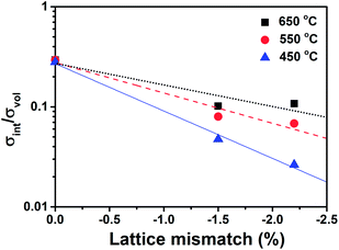 | ||
| Fig. 5 Normalized conductivity of the multilayers as a function of the lattice mismatch. Note that the y-axis scale is logarithmic. | ||
Schichtel et al. reported on the effect of compressive strain on oxygen ion conductivity in YSZ/Sc2O3 multilayers with lattice mismatch of −4.28%.13 The total conductivity was only decreased by a factor of ≈2 when the individual layer thickness decreased to 15 nm. This finding is similar to what is reported here for YDC/CZO45 multilayers with N = 3 (where the individual layer thickness is 15 nm), though the lattice mismatch at YSZ/Sc2O3 interface is nearly twice as large compared to that at the YDC/CZO45 interface. A large amount of interfacial strain seems to be released in YSZ/Sc2O3 multilayers since misfit dislocations were identified both at interfaces and in the volume regions.13 The energetic tradeoff between maintenance of mismatch strain and the nucleation of stress-relieving dislocations is likely to play a large role in determining the efficacy of using lattice mismatch to induce atomic strain and, thereby affect the ionic conductivity.
4. Conclusions
In this work, the effect of compressive strain on oxygen ion conductivity has been systematically studied in multilayers composed of YDC with CZO45, CZO30, and CeO2, respectively. The conductivity of YDC/CZO45 multilayers with lattice mismatch of −2.2% was monotonically decreased by at least one order of magnitude as the individual layer thickness approached interface sizes. As the lattice mismatch was decreased from −1.5% to near-zero for YDC/CZO30 to YDC/CeO2 multilayers, the conductivity approached that of bulk YDC. From a practical standpoint, the use of tensile strain to increase ionic conductivity is more useful. Multilayers consisting of YSZ and CZO provide means to study the effect of tensile strain on oxygen ion conductivity and are currently under investigation.Acknowledgements
Research supported by the U.S. Department of Energy, Office of Basic Energy Sciences, Division of Materials Sciences and Engineering under Award DE-SC0005403.References
- N. Q. Minh, J. Am. Ceram. Soc., 1993, 76, 563 CrossRef CAS PubMed.
- R. Doshi, V. L. Richards, J. D. Carter, X. P. Wang and M. Krumpelt, J. Electrochem. Soc., 1999, 146, 1273 CrossRef CAS PubMed.
- E. D. Wachsman and K. T. Lee, Science, 2011, 334, 935 CrossRef CAS PubMed.
- X. X. Guo and J. Maier, Adv. Mater., 2009, 21, 2619 CrossRef CAS.
- J. Garcia-Barriocanal, A. Rivera-Calzada, M. Varela, Z. Sefrioui, M. R. Diaz-Guillen, K. J. Moreno, J. A. Diaz-Guillen, E. Iborra, A. F. Fuentes, S. J. Pennycook, C. Leon and J. Santarnaria, ChemPhysChem, 2009, 10, 1003 CrossRef CAS PubMed.
- S. Ramanathan, J. Vac. Sci. Technol., A, 2009, 27, 1126 CAS.
- E. Fabbri, D. Pergolesi and E. Traversa, Sci. Technol. Adv. Mater., 2010, 11, 054503 CrossRef.
- N. Sata, K. Eberman, K. Eberl and J. Maier, Nature, 2000, 408, 946 CrossRef CAS PubMed.
- X. X. Guo, I. Matei, J. S. Lee and J. Maier, Appl. Phys. Lett., 2007, 91, 103102 CrossRef PubMed.
- X. X. Guo and J. Maier, Adv. Funct. Mater., 2009, 19, 96 CrossRef CAS.
- S. Azad, O. A. Marina, C. M. Wang, L. Saraf, V. Shutthanandan, D. E. McCready, A. El-Azab, J. E. Jaffe, M. H. Engelhard, C. H. F. Peden and S. Thevuthasan, Appl. Phys. Lett., 2005, 86, 131906 CrossRef PubMed.
- C. Korte, A. Peters, J. Janek, D. Hesse and N. Zakharov, Phys. Chem. Chem. Phys., 2008, 10, 4623 RSC.
- N. Schichtel, C. Korte, D. Hesse, N. Zakharov, B. Butz, D. Gerthsen and J. Janek, Phys. Chem. Chem. Phys., 2010, 12, 14596 RSC.
- S. Sanna, V. Esposito, A. Tebano, S. Licoccia, E. Traversa and G. Balestrino, Small, 2010, 6, 1863 CrossRef CAS PubMed.
- D. Pergolesi, E. Fabbri, S. N. Cook, V. Roddatis, E. Traversa and J. A. Kilner, ACS Nano, 2012, 6, 10524 CAS.
- B. Li, J. M. Zhang, T. Kaspar, V. Shutthanandan, R. C. Ewing and J. Lian, Phys. Chem. Chem. Phys., 2013, 15, 1296 RSC.
- C. Korte, N. Schichtel, D. Hesse and J. Janek, Monatsh. Chem., 2009, 140, 1069 CrossRef CAS PubMed.
- N. Schichtel, C. Korte, D. Hesse and J. Janek, Phys. Chem. Chem. Phys., 2009, 11, 3043 RSC.
- J. Garcia-Barriocanal, A. Rivera-Calzada, M. Varela, Z. Sefrioui, E. Iborra, C. Leon, S. J. Pennycook and J. Santamaria, Science, 2008, 321, 676 CrossRef CAS PubMed.
- X. Guo, Science, 2009, 324, 465 CrossRef CAS PubMed.
- A. Cavallaro, M. Burriel, J. Roqueta, A. Apostolidis, A. Bernardi, A. Tarancon, R. Srinivasan, S. N. Cook, H. L. Fraser, J. A. Kilner, D. W. McComb and J. Santiso, Solid State Ionics, 2010, 181, 592 CrossRef CAS PubMed.
- C. E. Hori, H. Permana, K. Y. S. Ng, A. Brenner, K. More, K. M. Rahmoeller and D. Belton, Appl. Catal., B, 1998, 16, 105 CrossRef CAS.
- Y. P. Fu, S. H. Hu and B. L. Liu, Ceram. Int., 2009, 35, 3005 CrossRef CAS PubMed.
- J. Jiang, W. D. Shen and J. L. Hertz, Thin Solid Films, 2012, 522, 66 CrossRef CAS PubMed.
- W. Shen, J. Jiang, C. Ni, Z. Voras, T. P. Beebe Jr and J. L. Hertz, Solid State Ionics, 2014, 255, 13 CrossRef CAS PubMed.
- M. Boaro, A. Trovarelli, J. H. Hwang and T. O. Mason, Solid State Ionics, 2002, 147, 85 CrossRef CAS.
- H. Inaba and H. Tagawa, Solid State Ionics, 1996, 83, 1 CrossRef CAS.
- H. Hayashi, R. Sagawa, H. Inaba and K. Kawamura, Solid State Ionics, 2000, 131, 281 CrossRef CAS.
- J. Jiang, X. C. Hu, W. D. Shen, C. Y. Ni and J. L. Hertz, Appl. Phys. Lett., 2013, 102, 143901 CrossRef PubMed.
- I. Kosacki and H. U. Anderson, Ionics, 2000, 6, 294 CrossRef CAS.
- V. Rührup and H.-D. Wiemhöfer, Z. Naturforsch., B: J. Chem. Sci., 2006, 61, 916 Search PubMed.
- A. Peters, C. Korte, D. Hesse, N. Zakharov and J. Janek, Solid State Ionics, 2007, 178, 67 CrossRef CAS PubMed.
- A. Kushima and B. Yildiz, J. Mater. Chem., 2010, 20, 4809 RSC.
| This journal is © The Royal Society of Chemistry 2014 |

