Fabrication of biocompatible high aspect ratio Au–Ni coaxial nanorod arrays using the electroless galvanic displacement reaction method

Che-Wei Hsua, Ching-Wen Lic and Gou-Jen Wang*abc
aDepartment of Mechanical Engineering, National Chung-Hsing University, Taichung 40227, Taiwan. E-mail: gjwang@dragon.nchu.edu.tw; Fax: +886-4-22877170; Tel: +886-4-22840725 Tel: +886-4-22840320
bGraduate Institute of Biomedical Engineering, National Chung-Hsing University, Taichung 40227, Taiwan
cPh.D. Program in Tissue Engineering and Regenerative Medicine, National Chung-Hsing University, Taichung 40227, Taiwan

Received 26th January 2014 , Accepted 19th February 2014

First published on 19th February 2014


Abstract

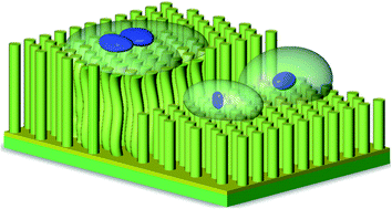
In this study, a novel method of fabrication of high aspect ratio magnetic Au–Ni coaxial nanorod arrays is proposed. The fabrication procedure involves anodic aluminum oxide (AAO) template preparation, barrier-layer surface photolithography, barrier layer etching, working electrode coating, nickel electroforming, alumina etching, and gold-plating by the electroless galvanic displacement reaction (EGDR) process. Experimental results have demonstrated that it is possible to synthesize high aspect ratio magnetic Au–Ni coaxial nanorod arrays using the method proposed in this study. The aspect ratio of the synthesized Au–Ni coaxial nanorod arrays was estimated to be 100–140. A two-dimensional electromagnetic force actuating system was set up to manipulate the 2-D movement of a patterned Au–Ni coaxial nanorod array. Biocompatibility of the proposed Au–Ni coaxial nanorod array was confirmed through the culture of endothelial cells (ECs) on the array surface. The influences of the stiffness of the nanorod array in terms of its height on cell morphology and differentiation were investigated. The results of the cell culture indicate that our Au–Ni coaxial nanorod array can be used to manipulate the differentiation of cells cultured on it by adjusting the array height.


1. Introduction

Recently, advances in the field of nanomaterials such as nanoparticles, nanowires, and nanorod arrays have paved the way for their various applications in optics, electronics, photoelectrics, and biomedicine.1,2 Compared to conventional planar materials and thin film materials, zero-dimensional or one-dimensional nanomaterials possess a much higher surface-to-volume ratio, hence offering a relatively larger sensing area to enhance detection sensitivity. Due to their special structures, one-dimensional nanostructures such as nanotubes, nanowires, and nanorods are more complicated to synthesize than zero-dimensional quantum dots and two-dimensional thin films. However, uniformly arranged nanorod arrays that have a comparatively larger surface-to-volume ratio are even more suitable for sensing applications.3–5

The fabrication techniques of one-dimensional nanomaterials can be categorized into two approaches: top-down and bottom-up.6,7 In the top-down approach, lithography, writing, or stamping techniques are used to carve and recompose the surface molecules of a bulk material. Soft lithography and dip-pen lithography are two of the more developed techniques in the top-down approach. On the contrary, the bottom-up approach uses spontaneous aggregation and binding characteristics between molecules or atoms to fabricate nanomaterials. Porous rod-like structures can be used as templates for the synthesis of nanorods or nano fibers. Anodic aluminum oxide (AAO) membranes, providing ordered porous arrays of regular hexagonal-shaped cells having nano-sized channels have been widely used as templates for fabricating one-dimensional nanomaterials, including carbon-nanotubes,8–11 carbon 60,12 Au nanorods,13–15 and Ni nanorods,16 or quantum dots.17–19 Hsu et al.20 have proposed an AAO template-based nano electroforming method for the fabrication of high aspect ratio (∼500) alumina–metal coaxial nanorod arrays with the diameter of the nanorod being 130 nm and the diameter of the inner nickel rod being 100 nm. The alumina outer layer of each individual metal nanorod serves as the insulator. The thickness of the alumina shell can be controlled by adjusting the etching duration.

Nickel is a material that can easily lead to allergies. The most commonly induced symptom of allergies is dermatitis.21 It was also reported that nickel can decrease the activity of DNA and RNA polymerase, hence reducing the duplication of DNA.22 In addition, Ni2+ can weaken the defense system of an organism, thereby enhancing the cancer-infection possibility of cells.23 Due to its high biocompatibility, gold, in particular its various nanostructures, has been widely used in biomedical applications. A high aspect ratio gold nanorod, which has a larger surface to volume ratio than that of a gold nanoparticle, is more suitable for biomedical applications, especially in biosensors.24–27 However, the relatively soft mechanical property of bulk gold limits the synthesis of high aspect ratio gold nanorods.

Considering both mechanical property and bio-compatibility, Au–Ni coaxial nanorods that integrate the advantages of nickel and gold may be a promising material for the development of efficient biosensors. Dolati et al.28 have reported that the ratio between Au and Ni in a gold–nickel alloy nanomaterial can be controlled by adjusting the deposition potential. Owing to the lower reduction potential of gold, the percentage of gold in the gold–nickel alloy nanomaterial can be increased using a lower synthesizing voltage. Yang et al.29 have found that the mechanical strength and wear resistance of the gold–nickel nanomaterial could be enhanced by increasing the nickel component. Chiu et al.30 have produced Ni–Au nanoparticles of a different ratio by adjusting the molar ratio of NiCl2 and HAuCl4 in the deposition solution. The influence of Au–Ni ratio on the cell survival rate using Au–Ni nanoparticles was further investigated for various Au–Ni ratios. It was concluded that the biocompatibility of the Au–Ni nanoparticles could not reach the level of pure Au nanoparticles even when the content of Au was largely increased. For effective bio-sensing applications, Au–Ni coaxial nanorods with a Ni-core and an Au-outer-shell possessing both the desired mechanical properties and bio-compatibility can offer a feasible solution.

In this research, a novel template based approach for the fabrication of a patterned array of Au–Ni coaxial nanorods was investigated. The orderly uneven barrier-layer surface of an AAO membrane was used as the template. The desired pattern was transferred to the barrier-layer by the photolithographic process. A thin Au film was deposited on the photolithographic patterned barrier-layer surface by evaporation, which was used as the electrode for further electrodepositing. Nickel nanorods were electroformed into nano channels in the patterned area. Phosphoric acid solution was then used to etch off the alumina of the AAO template to form a patterned nanostructure of bundles of nickel nanorods. Finally, the electroless nickel immersion gold (EGDR) method was used to form an Au shell wrapping each individual Ni nanorod.

2. Experimental section

2.1 Fabrication of high aspect ratio Au–Ni coaxial nanorod arrays

The sequences in the fabrication process of high aspect ratio Au–Ni coaxial nanorod arrays are schematically illustrated in Fig. 1 as AAO template preparation, working electrode coating, nickel electrodeposition, alumina etching, and gold-plating by the EGDR method. The details of each of these stages are described below.
image file: c4ra00773e-f1.tif
Fig. 1 Schematic illustration of the fabrication procedure. (A) AAO template preparation, (B) barrier-layer surface photolithography, (C) barrier layer etching, (D) working electrode coating and nickel electroforming, (E) alumina etching, and (F) electroless galvanic displacement reaction process and annealing.
(A) AAO template preparation. The AAO templates were prepared using a well-known anodizing process. Aluminum foils (99.9995% pure and 128 μm thick) were cleansed using ethanol and then acetone, followed by annealing at 400 °C for 3 hours in vacuum. Electropolishing was then carried out using a 1[thin space (1/6-em)]:[thin space (1/6-em)]4 perchloric acid and anhydrous ethanol solution as the electrolyte, under a constant voltage of 20 V for 2 minutes to further polish the surfaces of the foil. AAO films with a nanopore diameter of around 100 nm and a thickness of 60 μm were obtained by anodizing aluminum foils in a 0.3 M oxalic acid solution with an applied voltage of 90 V at 0 °C for 2 hours. The remaining aluminum beneath the barrier layer was dissolved in an aqueous CuCl2·HCl solution that was prepared by dissolving 13.45 g of CuCl2 powder in 100 mL of 35 wt% hydrochloric acid solution, revealing the honeycomb barrier-layer surface having an average convex diameter of 80 nm.20,31
(B) Barrier-layer surface photolithography. The barrier-layer surface was spin-coated with a 1 μm thick AZ 1518 positive photoresist layer. The parameters used for the spin coating are: spinning speed of the first stage = 500 rpm, spinning time for the first stage = 10 s, spinning speed of the second stage = 1500 rpm, spinning time for the second stage = 20 s; soft bake at 100 °C for 120 s; transfer of the desired pattern by UV exposure for 25 s and development using the AZ-300K developer for 30 s; hard bake at 120 °C for 180 s.
(C) Barrier layer etching. The barrier-layer surface was immersed in sodium hydroxide solution for 20 minutes to remove the patterned area of the barrier-layer surface.
(D) Au electrode deposition and nickel electroforming. A 20 nm thick gold electrode for electroforming was coated onto the barrier-layer side of the AAO template using the sputtering deposition technique. Next, a thin layer of nickel was added to the Au electrode surface by electroplating to increase the strength of the Au electrode.

Electroforming of nickel was carried out using a micro-electroforming system (EGG Instruments corporation/Model 263A) with a bulk nickel anode and the AAO template as the cathode, with a constant current of 0.01 A at 55 °C. Ni nanorods were electrodeposited from an aqueous solution of nickel sulfamate (Ni (NH2SO3·4H2O)) and chloride (NiCl4·7H2O) in boric acid (H3BO3).

(E) Alumina etching. The sample was immersed in a 1 M sodium hydroxide solution at room temperature to etch out the alumina. Subsequently, high aspect ratio nickel nanorods were obtained.
(F) Electroless galvanic displacement reaction (EGDR). EGDR is often used in printed circuit board industry to grow a thin layer of gold on a nickel substrate. Chemical reaction with the nickel is prevented by its displacement with gold, which protects the nickel from oxidation. When the nickel is immersed in the solution, it dissolves and emits two electrons. The gold then captures these electrons and gets deposited on the nickel surface. The reaction is gradually slowed down and finally stopped once the nickel surface is entirely covered with the gold. Generally, the ultimate deposition thickness of gold is about 100 nm. In this study, EGDR was used for electroless galvanic displacement of nickel by gold on the surface of each nickel nanorod.

Since metallic Ni easily oxidizes and forms nickel oxide on the surface, the sample was firstly immersed in a 5 wt% sulfuric acid solution to remove the surface oxide of the nickel nanorods. Then the samples were immersed in the immersion gold (IG) solution (ATOTECH, Germany) at 85 °C. The chemical reaction is as follows:

Ni + 2Au+ → Ni2+ + 2Au

The obtained crystalline structure and mechanical properties of the Au shell of the nanorods were weak but could be improved by an additional annealing process. This procedure involves heating the sample to 120 °C at the rate of 6 °C min−1, keeping the sample at this temperature for 2 hours, and then cooling the sample in the furnace to room temperature.32

2.2 Magnetic actuating system

Since the nickel core of the Au–Ni coaxial nanorods is a ferromagnetic material, a two-dimensional electromagnetic actuating force was used as the actuating source to enable 2-D movement of the patterned Au–Ni coaxial nanorod array. This system is composed of two sets of electromagnets. The two electromagnets were placed opposite to each other with each electromagnet being produced by wrapping 200 turns of ϕ 1 cm coil on a 10 cm steel rod. To enable 2-D vibration, the synthesized Au–Ni coaxial nanorod array was placed in the center of the actuating system. A programmable power supply was used to precisely control the electromagnetic force in the x and y directions.

Because the magnetic actuating system used in this study could not be placed in a SEM, optical microscopy (OM) was employed to observe the 2-D movement of the Au–Ni coaxial nanorod array.

2.3 Cell culture

To further investigate the biocompatibility of the synthesized material, non-patterned Au–Ni coaxial nanorod arrays were employed for the culture of human umbilical vein endothelial cells (HUVEC, BCRC). HUVECs were reserved in low glucose DMEM (Gibco, Invitrogen Co. Ltd) replenished with 10% (v/v) foetal bovine serum (FBS; Gibco, Invitrogen Co. Ltd), and 100 U mL−1 penicillin. The cells were cultured at 37 °C in an incubator containing 5% CO2. The medium was renewed every two days. Trypsinization on subcultures was performed using TrypLE Express (Gibco, Invitrogen Co. Ltd).

Before its use as the scaffold for cell seeding, the Au–Ni coaxial nanorod array was cleaned in 75% alcohol and phosphate buffered saline (PBS) in turns ten times and then put into a 24 well plate. Next, the cell suspension was diluted to 2 × 10⁴ cells per mL and added into each well. Finally, the cells were cultured at 37 °C in 5% CO2 for 2 days.

HUVECs were stained to observe the adhesion plaque and cell nucleus by immunofluorescence staining. The cells were fixed with 4% formaldehyde for 15 min. Then, the cells were treated with 0.5% Triton-X 100 for 10 min for permeability. 1% bovine serum albumin (BSA) was added for blocking the non-specific site for 30 min. The vinculin affinity recombinant rabbit monoclonal antibody was diluted with 1[thin space (1/6-em)]:[thin space (1/6-em)]1000 as the primary antibody and was used to bind the cell adhesion plaque for 1 h. The second antibody, Alexa Fluor 488 goat anti-rabbit antibody was used for binding with the primary antibody for 1 h for coloration. The cell nucleus was stained with Hoechst 33258 for 10 min. During each step, PBS was used for washing three times. A fluorescence microscope (LEICA inverted microscopy, DMI6000B) was used to observe the cell morphology.

3. Results and discussion

3.1 Au–Ni coaxial nanorod array fabrication results

Fig. 2 illustrates the SEM images of a prepared AAO barrier layer surface, a patterned barrier layer surface, a non-patterned nickel nanorod array, and a patterned nickel nanorod array. A uniformly distributed hemisphere array formed the barrier layer of the synthesized AAO (Fig. 2A). As can be seen in Fig. 2B, the AZ 1518 positive photoresist could well protect the non-patterned area and the desired patterns could be completely transferred to the barrier layer surface of the AAO template. The average diameter of the Ni nanorods which formed the non-patterned nickel nanorod array shown in Fig. 2C was about 100 nm, which is consistent with that of the nano channel of the synthesized AAO membrane. It can be observed from Fig. 2D that the designed pattern was successfully transferred to the barrier layer surface and a nickel nanorod array with a desired pattern could be electroformed.
image file: c4ra00773e-f2.tif
Fig. 2 SEM illustrations of the nickel nanorod array fabrication results. (A) The barrier layer surface of a synthesized AAO membrane, (B) the patterned barrier layer surface, (C) the non-patterned nickel nanorod array, and (D) the patterned nickel nanorod array.

Fig. 3 displays the SEM images of the Au–Ni coaxial nanorod arrays synthesized through different EGDR processing times. Four different processing times viz. 3 min, 5 min, 10 min, and 20 min, were used and the corresponding results are shown in Fig. 3(A) to (D) with the average diameters of these synthesized Au–Ni coaxial nanorod arrays estimated to be about 210 nm, 230 nm, 260 nm, and 300 nm, respectively. The respective thicknesses of the grown gold shells were estimated to be 55 nm, 65 nm, 80 nm, and 100 nm, respectively. Fig. 3E further presents the relationship between the grown gold shell thickness and the EGDR processing times. During the early stages of the EGDR process, the gold cations in the EGDR solution could fully access the surface of each nickel nanorod to acquire the required electrons for reduction. Hence, the growth rate of the gold shell was high. After about 3 min of immersion, most of the nickel nanorod surface was covered with gold; therefore, the gold shell gradually grew to attain the ultimate thickness of 100 nm. The observation indicates that the thickness of the outer gold shell can be well controlled by varying the EGDR processing time. Since the average height of the synthesized Au–Ni coaxial nanorod arrays was about 30 μm, the aspect ratio of the coaxial nanorod arrays was calculated to be about 100 to 140. Fig. 2F further presents the annealed Au–Ni coaxial nanorod array corresponding to the 5 min EGDR processed nanorod array shown in Fig. 2B. It can be observed that the annealing process modified the surface of the nanorod from a rough to a more even and smoother surface.


image file: c4ra00773e-f3.tif
Fig. 3 SEM images of the synthesized Au–Ni coaxial nanorod arrays corresponding to different EGDR processing times given by (A) processing time = 3 min; (B) processing time = 5 min; (C) processing time = 10 min; (D) processing time = 20 min. (E) Relationship between the gold shell thickness and the EGDR processing time and (F) annealed Au–Ni coaxial nanorod array corresponding to the 5 min EGDR processed nanorod array shown in (B).

Fig. 4 shows the X-ray diffraction (XRD) analysis results of four samples of the synthesized Au–Ni coaxial nanorod array. These four samples were: Ni nanorod array, Au–Ni coaxial nanorod array with a 3 min EGDR process, annealed Au–Ni coaxial nanorod array of the 3 min EGDR sample, and the Au–Ni coaxial nanorod array with a 5 min EGDR process. The XRD analysis results indicate that except the Ni nanorod array, the three other samples contained Au element after an EGDR process. A longer EGDR process could increase the Au content in the Au–Ni coaxial nanorod array. The particle size of the deposited gold can be calculated by Scherrer equation below:

image file: c4ra00773e-t1.tif
where τ denotes the particle size (nm); K is the dimensionless shape factor (0.89); λ is the X-ray wavelength (0.154056 nm); β denotes the line broadening at half the maximum intensity (FWHM) (radians); θ represents the Bragg angle. The particle size of the deposited gold under a 3 min EGDR process was calculated to be about 15.2 nm. After annealing, the particle size was reduced to 12.5 nm, agreeing with the SEM image shown in Fig. 3F. The results implied that that the annealing process could refine the lattice of the deposited gold particles.


image file: c4ra00773e-f4.tif
Fig. 4 XRD analysis results of four Au–Ni coaxial nanorod array samples.

3.2 Two dimensional movements of the patterned Au–Ni coaxial nanorod array

To enable distinct observation of the 2-D movement, a patterned Au–Ni coaxial nanorod array as shown in Fig. 5 was fabricated. The diameter of each patterned circle area was 6 μm and the pitch of the pattern was 60 μm. The height of the Au–Ni coaxial nanorod arrays with a 3 min EGDR process is 30 μm. The dotted lines in these four OM images shown in Fig. 5 indicate the neutral position of the patterned bundles of the Au–Ni coaxial nanorod. It can be seen from these four OM images that the patterned bundles of the Au–Ni coaxial nanorod could be actuated by the magnetic actuation system to swing in both x and y directions. Movies for nanoscale 2D swing and rotation of the Au–Ni coaxial nanorods driven by the two-dimensional electromagnetic actuating system were illustrated in Movie S1 and S2, respectively.
image file: c4ra00773e-f5.tif
Fig. 5 OM demonstration of the 2-D motion of a patterned Au–Ni coaxial nanorod array.

It has been reported that it is possible for cell surface receptors to deliver a shear stress stimulus into cells through the cytoskeleton so that the functional performance of cells can be affected.33,34 In our previous work, it was observed that a suitable shear stress could tremendously enhance endothelial cell proliferation.35 It is possible that stem cells may differentiate to different functional cells under different shear stress stimuli. The synthesized Au–Ni coaxial nanorod array in this study, which enables a controllable shear stress to be induced by the nanoscale 2D swing and rotation, which are driven by an electro-magnetic field, can be a useful scaffold for investigating cell differentiation.

3.3 Cell culture results

As reported by Chiu et al.,30 Au–Ni nanoparticles were not completely biocompatible even when the content of Au was largely increased. The biocompatibility of our Au–Ni coaxial nanorod arrays was illustrated by the two-day EC culture results shown in Fig. 6. The results indicate that the ECs adhered well to the array surface after having been cultivated for two days. The Au–Ni coaxial nanorod array synthesized in this study with each Ni nanorod completely wrapped by a thin Au shell should prevent the Ni material from contacting the cells cultured on the array surface. Therefore, biocompatibility could be achieved.
image file: c4ra00773e-f6.tif
Fig. 6 SEM images of the ECs cultured on the synthesized Au–Ni coaxial nanorod arrays of height (A) 25 μm and (B) 30 μm.

It has also been reported that the stiffness of a scaffold could affect the morphology, focal adhesions, cytoskeletal contraction, and differentiation of the culture cells.36,37 The unique focal adhesion characteristics of stem cells, which promote cytoskeletal contraction under a particular stiffness scaffold, results in the differentiation of stem cells to different functional cells.38 Our high aspect ratio Au–Ni coaxial nanorod array, which enables controllable stiffness by adjusting the height of the nanorod array, can also be a useful tool for effectively controlling of cell proliferation. Therefore, Au–Ni coaxial nanorod arrays with 3 min EGDR process of two different heights viz. 25 μm and 30 μm were further employed for the preliminary investigation of the stiffness influences on cell morphology and cell division. The stiffness of the scaffolding array is inversely proportional to the array height.

The immunofluorescence images for cell morphology are displayed in Fig. 7. From the DAPI staining, it can be observed that the cell nucleus divided on the 30 μm Au–Ni coaxial nanorod array after days of culture, implying that the cell was in proliferate progress. It is also observed from the SEM images of Fig. 6 and 7 that the cell expanded more on the higher nanorod array. It suggests that HUVECs tend to grow well on a softer matrix because the natural environment of endothelial cells is a relatively stiffer environment.39 These HUVEC culture results reveal that our Au–Ni coaxial nanorod array could be used to manipulate the differentiation of cells cultured on it.


image file: c4ra00773e-f7.tif
Fig. 7 Fluorescence images of the ECs cultured on the Au–Ni coaxial nanorod arrays having heights of (A) 25 μm and (B) 30 μm.

Theoretically, the horizontal displacement x at the tip of the Au–Ni coaxial nanoelectrode can be represented by x = 64FL3/3πEd4 when a horizontal force F is applied to an Au–Ni coaxial nanorod, where E, L, and d denote the Young's modulus, length, and diameter of the nanorod, respectively. The horizontal displacement subjected to a constant horizontal force can be used to represent the softness of an Au–Ni coaxial nanorod. When a nanorod array is used as a scaffold for cell culture, the contraction force of the cells during expansion provides a horizontal force to each nanorod adhering to the cells. Since our Au–Ni coaxial nanorod has an aspect ratio (L/d) of up to 140 and a nanoscale diameter, even a tiny contraction force from the cultured cells can cause a visible horizontal displacement at the nanorod tip. The horizontal displacement can be easily controlled by the length of the nanorod array i.e., the stiffness of the nanorod array based scaffold can be easily controlled by adjusting the length of the nanorod array. Compared to the reported lower aspect ratio (∼6) micropost array of PDMS,36,37 our biocompatible Au–Ni coaxial nanorod array enables a larger range of lower stiffness values for a more precise control of stem cell differentiation. Furthermore, since the stiffness of the nanorod array based scaffold remains constant during the entire cell culture process without influence from the contents of the culture medium, an analysis of the stiffness based induced differentiation can be easily conducted. The Au–Ni coaxial nanorod array will be further implemented for effectively inducing stem cell differentiation.

4. Conclusions

Due to its high biocompatibility, gold, especially its various nanostructures, has been widely used in biological applications. Considering both the desired mechanical property and biocompatibility, this study proposes a novel approach for the fabrication of a patterned array of Au–Ni coaxial nanorods using the barrier-layer surface of an AAO membrane as the template. A two-dimensional magnetic force was employed as the actuating source to drive the patterned Au–Ni coaxial nanorod array for moving in both x and y directions. Because of the ferromagnetic characteristics of the Ni core, the 2-D movement of the Au–Ni nanorod array could be manipulated by the magnetic force. Biocompatibility of the proposed Au–Ni coaxial nanorod array was confirmed through the culture of ECs on the array surface. Preliminary investigation of the influences of the array stiffness in terms of its height on cell morphology and cell division were conducted. The cell culture results indicate that the cell expanded more on the higher nanorod array. The Au–Ni coaxial nanorod array will be further investigated for effectively inducing stem cell differentiation.

Acknowledgements

The authors would like to offer their thanks to the National Science Council of Taiwan under grant number NSC-101-2212-E-005-022-MY3 for their financial support of this research.

References

  1. B. Y. Kim, J. T. Rutka and W. C. Chan, N. Engl. J. Med., 2010, 363, 2434–2443 CrossRef CAS PubMed.
  2. R. Subbiah, M. Veerapandian and K. S. Yun, Curr. Med. Chem., 2010, 17, 4559–4577 CrossRef CAS.
  3. G. Cao and D. Liu, Adv. Colloid Interface Sci., 2008, 136, 45–64 CrossRef CAS PubMed.
  4. G.-J. Wang and H.-T. Chen, Curr. Nanosci., 2009, 5, 297–301 CrossRef CAS.
  5. Y. Li, N. Koshizaki and W. Cai, Coord. Chem. Rev., 2011, 255, 357–373 CrossRef CAS PubMed.
  6. B. D. Gates, Q. Xu, M. Stewart, D. Ryan, C. G. Willson and G. M. Whitesides, Chem. Rev., 2005, 105, 1171–1196 CrossRef CAS PubMed.
  7. B. K. Teo and X. Sun, J. Cluster Sci., 2006, 17, 529–540 CrossRef CAS PubMed.
  8. Y. Yun, A. Bange, W. R. Heineman, H. B. Halsall, V. N. Shanov, Z. Dong, S. Pixley, M. Behbehani, A. Jazieh and Y. Tu, Sens. Actuators, B, 2007, 123, 177–182 CrossRef CAS PubMed.
  9. S. Sigurdson, V. Sundaramurthy, A. Dalai and J. Adjaye, J. Mol. Catal. A: Chem., 2009, 306, 23–32 CrossRef CAS PubMed.
  10. H.-J. Ahn, J. I. Sohn, Y.-S. Kim, H.-S. Shim, W. B. Kim and T.-Y. Seong, Electrochem. Commun., 2006, 8, 513–516 CrossRef CAS PubMed.
  11. S. Rajaputra, R. Mangu, P. Clore, D. Qian, R. Andrews and V. P. Singh, Nanotechnology, 2008, 19, 345502 CrossRef PubMed.
  12. C. J. Li, X. S. Gao and X. N. Li, J. Macromol. Sci., Part A: Pure Appl. Chem., 2006, 43, 1679–1685 CrossRef CAS.
  13. L. Liu, W. Lee, Z. Huang, R. Scholz and U. Gösele, Nanotechnology, 2008, 19, 335604 CrossRef CAS PubMed.
  14. T.-Y. Shin, S.-H. Yoo and S. Park, Chem. Mater., 2008, 20, 5682–5686 CrossRef CAS.
  15. F. Li and J. B. Wiley, J. Mater. Chem., 2008, 18, 3977–3980 RSC.
  16. R. Inguanta, S. Piazza and C. Sunseri, Electrochim. Acta, 2008, 53, 5766–5773 CrossRef CAS PubMed.
  17. C. C. Chen, Y. C. Liu, C. H. Wu, C. C. Yeh, M. T. Su and Y. C. Wu, Adv. Mater., 2005, 17, 404–407 CrossRef CAS.
  18. C. L. Feng, X. H. Zhong, M. Steinhart, A. M. Caminade, J. P. Majoral and W. Knoll, Small, 2008, 4, 566–571 CrossRef CAS PubMed.
  19. D. Cui, B. Pan, H. Zhang, F. Gao, R. Wu, J. Wang, R. He and T. Asahi, Anal. Chem., 2008, 80, 7996–8001 CrossRef CAS PubMed.
  20. C.-W. Hsu, Z.-D. Chou and G.-J. Wang, J. Microelectromech. Syst., 2010, 19, 849–853 CrossRef CAS.
  21. L. Mattila, M. Kilpeläinen, E. O. Terho, M. Koskenvuo, H. Helenius and K. Kalimo, Contact Dermatitis, 2001, 44, 218–223 CrossRef CAS.
  22. K. Wang, Element in Life, Chinese Metrotogy publishing Company, 1992 Search PubMed.
  23. Y. Ren, K. Yang and Y. Liang, J. Biomed. Eng., 2005, 22, 1067 CAS.
  24. X. Huang, I. H. El-Sayed, W. Qian and M. A. El-Sayed, J. Am. Chem. Soc., 2006, 128, 2115–2120 CrossRef CAS PubMed.
  25. C. Yu and J. Irudayaraj, Anal. Chem., 2007, 79, 572–579 CrossRef CAS PubMed.
  26. N. J. Durr, T. Larson, D. K. Smith, B. A. Korgel, K. Sokolov and A. Ben-Yakar, Nano Lett., 2007, 7, 941–945 CrossRef CAS PubMed.
  27. K. M. Mayer, S. Lee, H. Liao, B. C. Rostro, A. Fuentes, P. T. Scully, C. L. Nehl and J. H. Hafner, ACS Nano, 2008, 2, 687–692 CrossRef CAS PubMed.
  28. A. Dolati, M. Ghorbani and M. Ahmadi, J. Electroanal. Chem., 2005, 577, 1–8 CrossRef CAS PubMed.
  29. Z. Yang, D. J. Lichtenwalner, A. S. Morris, J. Krim and A. I. Kingon, J. Microelectromech. Syst., 2009, 18, 287–295 CrossRef CAS.
  30. H.-K. Chiu, I.-C. Chiang and D.-H. Chen, J. Nanopart. Res., 2009, 11, 1137–1144 CrossRef CAS.
  31. S.-K. Hwang, S.-H. Jeong, H.-Y. Hwang, O.-J. Lee and K.-H. Lee, Korean J. Chem. Eng., 2002, 19, 467–473 CrossRef CAS.
  32. T. Whitney, P. Searson, J. Jiang and C. Chien, Science, 1993, 261, 1316–1319 CAS.
  33. C. Zaragoza, S. Márquez and M. Saura, Curr. Opin. Lipidol., 2012, 23, 446–452 CrossRef CAS PubMed.
  34. C. Gaucher, C. Devaux, C. Boura, P. Lacolley, J.-F. Stoltz and P. Menu, Clin. Hemorheol. Microcirc., 2007, 37, 99–107 CAS.
  35. C.-W. Li and G.-J. Wang, Biofabrication, 2013, 5, 045001 CrossRef PubMed.
  36. J. L. Tan, J. Tien, D. M. Pirone, D. S. Gray, K. Bhadriraju and C. S. Chen, Proc. Natl. Acad. Sci. U. S. A., 2003, 100, 1484–1489 CrossRef CAS PubMed.
  37. J. Fu, Y.-K. Wang, M. T. Yang, R. A. Desai, X. Yu, Z. Liu and C. S. Chen, Nat. Methods, 2010, 7, 733–736 CrossRef CAS PubMed.
  38. A. J. Engler, S. Sen, H. L. Sweeney and D. E. Discher, Cell, 2006, 126, 677–689 CrossRef CAS PubMed.
  39. M. Cecelja and P. Chowienczyk, J. R. Soc. Med. Cardiovasc. Dis., 2012, 1 Search PubMed.

Footnote

Electronic supplementary information (ESI) available. See DOI: 10.1039/c4ra00773e

This journal is © The Royal Society of Chemistry 2014
Click here to see how this site uses Cookies. View our privacy policy here.