DOI:
10.1039/C4RA00164H
(Communication)
RSC Adv., 2014,
4, 22246-22250
Stable field emission lamps based on well-aligned BaO nanowires
Received
8th January 2014
, Accepted 2nd May 2014
First published on 8th May 2014
Abstract
Well-aligned BaO nanowires were synthesized on ITO glass substrates by a hydrothermal process. The morphology and composition of the BaO nanowires were characterized by field emission scanning electron microscopy, high resolution transmission electron microscopy, selected area electron diffraction, X-ray diffraction, and energy dispersive X-ray spectroscopy. The results confirmed that BaO nanowires had single crystalline cubic structures and grew along the [111] direction. The well-aligned BaO nanowires show superior field emission properties, and exhibited a low turn-on field (∼0.9 V μm−1), a low threshold field (∼3.59 V μm−1), a high field enhancement factor (β = 2463), and a good stability of the emission current. The field emission lamps fabricated by using the BaO nanowires as emitters display uniform and bright emission patterns under the diode mode. These results demonstrate that such BaO nanowires are promising for application in practical flat panel displays.
1. Introduction
Field emission (FE) is one of the main features of nanostructures, in which electrons are injected from the surface of the material into vacuum under an applied electric field.1–4 Over the past decade, one dimensional (1D) nanostructures, such as carbon nanotubes and ZnO nanowires with excellent field emission characteristics have attracted much attention due to their potential applications in a wide range of field emission devices, such as X-ray tubes, high power microwave amplifiers, flat panel displays, backlighting, and other vacuum microelectronic devices.5–9 In order to make highly efficient FE devices feasible for further commercial applications, there are two approaches to achieve this goal. On one hand, lowered work function of the emitters can increase the field enhancement and improve the field emission characteristics according to Fowler–Nordheim (F–N) theory.10 For example, Pandey et al.11,12 has reported that modification of the surface states of emitters, such as surface coating and decoration, can improve their field emission properties owing to their decreased work function. On the other hand, the morphology of nanostructures has been found to play an important role in the field emission performance. For example, Xu et al.13,14 has found that the FE devices based on nanoneedles with the smallest emitter radius have the lowest turn-on field and the largest FE current density, which is due to the increased field enhancement factor. Therefore, novel nanostructure material with lower work function or new architecture of nanostructure is desirable to explore efficient FE devices.
Barium oxide (BaO), an important direct band gapII–VI semiconductor, has a wide band gap of 4.4 eV, high thermal stability, robust mechanical strength, and oxidation resistance in harsh environments, therefore, it is considered as a potential application in the FE devices. In particular, the work function of BaO (1.44 eV)15 is lower than that of many field emission materials, such as carbon nanotubes (5.0 eV)16 and ZnO (5.3 eV),16 which is expected to enhance the field emission performance. BaO nanostructures have been studied to obtain higher photoemission from these nanoparticles by Yang.17 However, to the best of our knowledge, there has been no report on the field emission properties of BaO nanostructures. Herein, we shall present the fabrication of FE devices and FE lamps with well-aligned BaO nanowires by a simple hydrothermal synthesis process. The field emission properties of the BaO nanowires were analyzed and characterized. Our results would be helpful for the design, fabrication, and optimization of the BaO nanostructures as field emitters.
2. Experiment
Indium tin oxide (ITO) glass (20 Ω □−1) was used as the substrate. All chemicals used were purchased from Aldrich. Firstly, ITO glass substrates were ultrasonically soaked in de-ionized water, acetone, and iso-propanol alcohol subsequently, and then dried at 100 °C in a laboratory oven. Afterwards, a 10 nm BaO seed layer was deposited on the ITO glass substrates by the ultrasonic spray pyrolysis (USP) method.18 ITO glass substrates were then immersed into a mixture solution of 0.02 M barium nitrate hexahydrate and 0.02 M hexamethylenetetramine (HMT). ITO substrate was faced downwards immersed in the solution. The growth was carried out at 95 °C. After 6 hours, the sample was taken out, washed and dried.
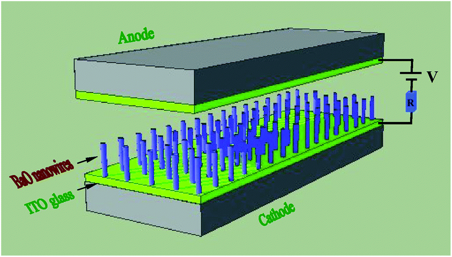
The field emission measurement was performed with a simple diode configuration in a vacuum chamber which was pumped down to 10−4 Pa at room temperature (see Fig. 1). The cathode was the as-prepared BaO nanowires on ITO glass and the anode was ITO glass coated with a layer of fluorescent powder with different colors. The inter-electrode distance of diode was kept constant by a 1 mm ceramic spacer. The measured emission area was about 10 × 10 mm2. The emission current was measured as a function of voltage: a DC-voltage between cathode and anode. The data were recorded only after ramping up and down the applied voltage at least five times (electrical annealing) to stabilize the electron emission.
 |
| | Fig. 1 Schematic diagram of a simple diode configuration for measuring FE properties of BaO nanowires. | |
3. Results and discussion
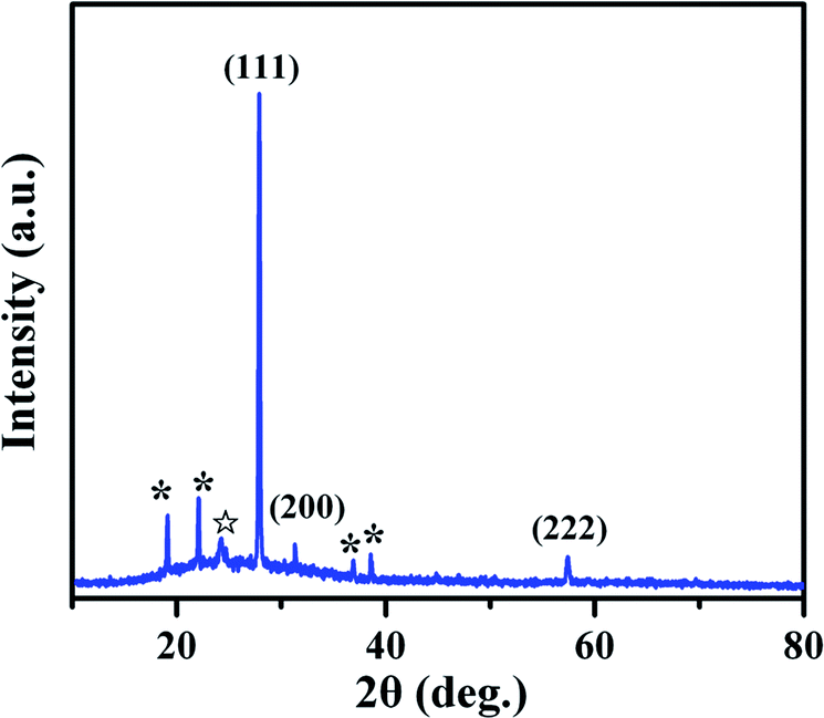
Fig. 2 shows the typical X-ray diffraction (XRD) patterns of the as-grown BaO nanowires. It can be seen that, except for the peaks of ITO substrate (labeled by ☆) and that of the residual barium nitrate (labeled by *), all the diffraction peaks can be well indexed to the cubic structured BaO with cell parameters a = b = c = 0.55 nm, which is in good agreement with the literature values (JCPDS card no. 01-0746). No characteristic diffraction peaks of other impurities could be detected, indicating high purity of BaO phase. It demonstrates that the BaO nanowires have good crystalline. In addition, the intensity of the (111) diffraction is much stronger than that of other peaks, indicating that the BaO nanowires possess a preferred orientation along the [111] direction.
 |
| | Fig. 2 XRD patterns of BaO nanowires. | |
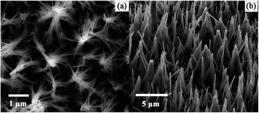
The crystal morphology of the as-grown BaO nanowires is characterized by using FESEM. Fig. 3(a) and (b) show the top-view and tilted cross-section-view SEM images of the sample. The length of the nanowires is estimated to be approximately 4–5 μm, and the diameter of the single BaO nanowire is around 90 nm and the tip radius is about 30 nm; hence the diameter to length ratio is 40–50. The BaO nanowires are well vertically aligned on the substrate with uniform size. Meanwhile, several nanowires converge into a tip, all of which are uniformly distributed. It is worth noting that BaO nanowires can also be grown on the FTO, PET substrate using the similar method. The substrate plays little effect on morphology of the BaO nanowires. Meanwhile, the thickness of seeding layer may produce some effect on the morphology of BaO, further change the field emission property of BaO nanostructure. We will continue to study on it in our next step.
 |
| | Fig. 3 (a) Top-view and (b) tilted cross-section-view SEM images of the as-grown BaO nanowires. | |
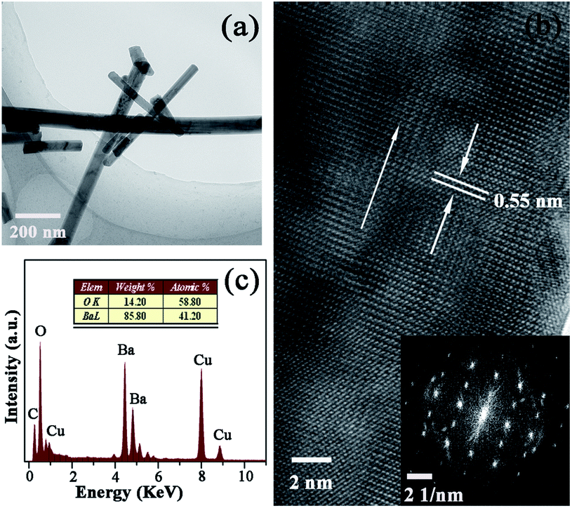
The crystal structure and morphology of the single BaO nanowire are further characterized by transmission electron microscopy (TEM). Fig. 4(a) shows the low-magnification TEM image of the BaO nanowires scraped from ITO substrate, exhibiting the typical 1D nanostructure with smooth surface. From the TEM image, it can be seen that the BaO nanowire is straight and uniform with a diameter of about 90 nm, which is consistent with the results of the SEM images [Fig. 3(a) and (b)]. Fig. 4(b) displays a corresponding high-resolution TEM (HRTEM) image taken from the BaO nanowire labeled in Fig. 4(a), which shows a typical lattice structure. The selected area of electron diffraction (SAED) pattern [Fig. 4(b)] indicates that the BaO nanowire is a single crystal structure with the lattice distance of 0.55 nm, implying the exposed (111) facet. The energy dispersive X-ray spectroscopy (EDX) result [see Fig. 4(c)] shows that the nanowire is composed of O and Ba with an atomic ratio of close to 1![[thin space (1/6-em)]](https://www.rsc.org/images/entities/char_2009.gif) :1, confirming that the nanowire is BaO. The C and Cu signals come from the supporting TEM carbon-coated copper grid.
:1, confirming that the nanowire is BaO. The C and Cu signals come from the supporting TEM carbon-coated copper grid.
 |
| | Fig. 4 (a) Low-magnification TEM image of the BaO nanowires; (b) HRTEM image and SAED pattern of as-grown sample; (c) EDX result of the BaO nanowires. | |
The growth process of BaO nanowires is proposed as follows: firstly, a thin layer of BaO seeds was grown on the substrate by the USP method; secondly, thermal degradation of HMT releases hydroxyl ions which react with Ba2+ ions to form BaO. The chemical reactions can be summarized by the following equations:19
| | |
C6H12N4 + 6H2O ↔ 6HCHO + 4NH3
| (1) |
| | |
NH3 + H2O ↔ NH4+ + OH−
| (2) |
| |
 | (3) |
HMT is the source of alkali to supply the hydroxyl ions to drive the precipitation reaction from eqn (1) and (2). In the initial growth stage, the high pH value forces the eqn (3) to move to the right and the Ba2+ ions are changed to Ba(OH)2. With gradual increase of pH value, Ba(OH)2 becomes thermodynamically unstable and the Ba(OH)2 begins to grow on the substrate at 95 °C. Subsequently, BaO nanowires can be grown out as the Ba(OH)2 transfers to the solid precipitate.19 The less thermodynamically stable the phase is, the faster speed the solid has to precipitate out.20
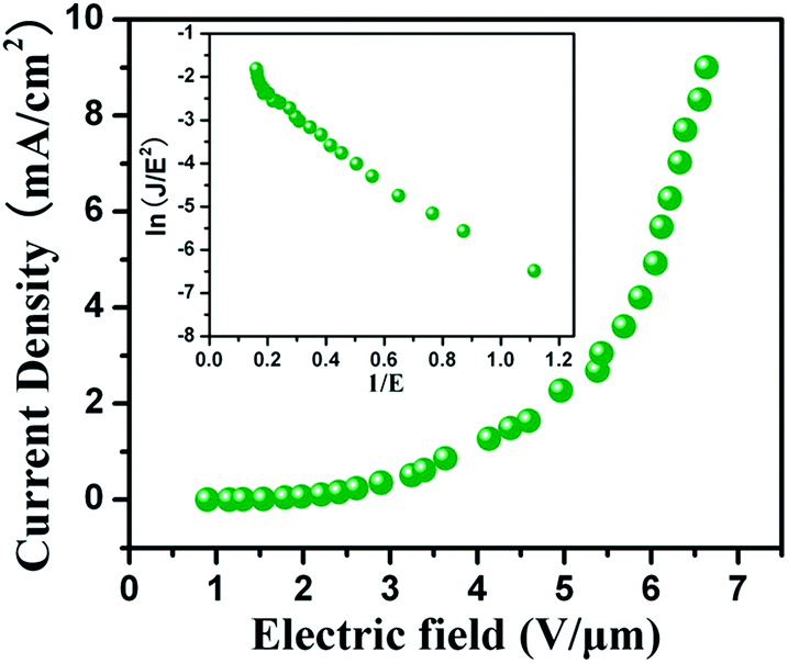
Fig. 5 shows the relationship between the measured field emission current density (J) and the applied electric field (E) for the BaO nanowires. It is clear that the BaO emitters have the turn-on field (defined as E which is the field required to produce the J of 10 μA cm−2) of ∼0.9 V μm−1, and the threshold field (defined as E which is the field required to produce the J of 1 mA cm−2) of ∼3.59 V μm−1. The FE devices based on 1D nanostructures have been reported previously. Xu et al. have reported the turn-on field of 1.7 V μm−1 and the threshold field of 4.8 V μm−1 for ZnO nanoawl arrays,13 and Lee et al. have presented the turn-on field of 1.39 V μm−1 and the threshold field of 3.67 V μm−1 for point-type carbon nanotubes.21 A summary of the FE devices is compared in Table 1. Obviously, the performance of FE device obtained in this paper is comparable. Although the turn-on field and threshold field of BaO nanowires in this paper are worse than those of the graphene/double walled CNTs (DWCNTs) nanostructures emitters, the fabrication of BaO nanowires has a simple process.25 The superior emission results can be attributed to the lower work function and the high aspect ratio of the nanowires with axial growth. In the previous study, it is found the high density nanowire structure may lead to the high electric shielding. In this study, The density of BaO nanowires on the substrate surface is quite low, for this reason, electric shielding effect could be alleviated.26
 |
| | Fig. 5 Field emission current density as a function of applied electric field for the BaO nanowires. The inset is the corresponding F–N plot. | |
Table 1 A comparison of FE parameters of various nanostructures in literatures and in this paper
| Field emitters |
Turn-on field (at 10 μA cm−2) |
Threshold field (at 1 mA cm−2) |
Reference |
| ZnO nanoawl |
1.7 V μm−1 |
4.8 V μm−1 |
13 |
| CNTs |
1.39 V μm−1 |
3.67 V μm−1 |
21 |
| ZnO–graphene |
2.7 V μm−1 |
5.1 V μm−1 |
22 |
| Graphene sheets |
1.56 V μm−1 |
5.12 V μm−1 |
23 |
| α-Fe2O3/CNTs |
1.21 V μm−1 |
3.23 V μm−1 |
24 |
| Graphene/DWCNTs |
0.62 V μm−1 |
1.19 V μm−1 |
25 |
| BaO nanowires |
0.9 V μm−1 |
3.59 V μm−1 |
This work |
To further analyze the emission properties of the above-mentioned emitters, the corresponding Fowler–Nordheim (FN) plot is shown in the inset of Fig. 5, which exhibits linear behavior. The emission current density (J) and applied field (E) characteristics can be analyzed by FN equation for the FE as follows,10,27
| |
 | (4) |
where
J is the current density in mA cm
−2,
E is the applied field strength in V μm
−1,
A and
B are constants being 1.56 × 10
−10 A V
−2 eV and 6.83 × 10
3 V eV
−3/2 μm
−1, respectively.
φ is the work function of the emitter that is related to the surface states, and
β is the so-called field enhancement factor that is introduced to reflect the degree of the FE enhancement of any tip over a flat surface. The inset in
Fig. 5 shows the ln(
J/
E2) − 1/
E plot for the BaO sample. The plot exhibits quasi-linear dependence, indicating that the FE from BaO nanowires follows the F–N relation. According to the slopes of fitting curves, the
β is estimated to be 2463 for BaO nanowires emitters, if we assume that
φ = 1.44 eV. The FE enhancement factor of the BaO emitters is rather high compared to other nanostructure emitters reported previously. It is found that the FE enhancement factor of about 1537 for ZnO nanowire emitters,
28 642 for ZnO nanowire synthesized by vapor–solid process,
29 896 for ZnO nanorod synthesized on ITO substrate,
30 and about 720 for a ZnO nanotips.
31 The field enhancement factor (
β) is introduced to reflect the degree of the field emission enhancement of any tip over a flat surface. Besides experimental
β value that obtained from the FN-plot, there is another one called intrinsic
β value which could be calculated by
β =
h/
r, where
h is the height of the tip and
r is the radius of curvature of the tip apex. Therefore, the obtained high enhancement factor may be ascribed to the structure of the BaO nanowires, their orientation to the substrate, and the high aspect ratio.
32 Therefore, 1D BaO nanowire has the potential to be considered as the excellent field emitters with the high enhancement factor and low turn-on field and threshold field.
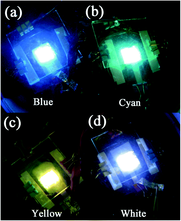
Thus, we evaluated the feasibility of FE lamps using the BaO nanowire emitters. A simple diode configuration is used in the lamp. The cathode was the as-prepared BaO nanowires on ITO glass and the anode was ITO glass coated with a layer of fluorescent powder. The distance between cathode and anode is about 1 mm. The FE lamp has a square shape and the active area is approximately 10 × 10 mm2. Fig. 6 shows emission patterns from the lamps made using the BaO nanowire emitters with blue, cyan, yellow, and white color. The emission pattern of the square lamps is obtained at an applied electric field of 5.7 V μm−1. The emission is pretty uniform and bright with the luminance of higher than 500 cd m−2. It is worth noting our lamps display good FE performance, which is still necessary to be measured in a vacuum chamber under continuous vacuum pumping at a reasonably high vacuum pressure. The BaO nanowire emitters described here will be used for FE devices at a low vacuum pressure in future study.
 |
| | Fig. 6 Emission patterns of the lamps made using the BaO nanowires emitters under diode mode. The lamps show uniform and bright emission patterns with different colors: (a) blue, (b) cyan, (c) yellow, and (d) white. | |
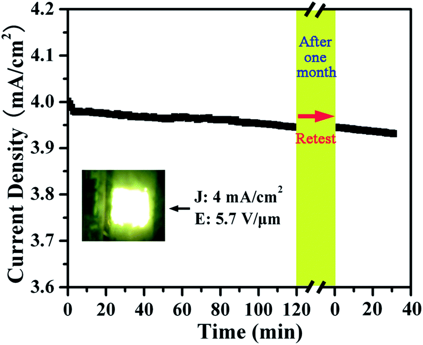
Finally, to check the robustness of the present BaO nanowires, the FE lifetime and stability are also paramount issues in FE devices. We have conducted lifetime measurements at a pressure of 10−4 Pa with an initial emission current density J of 4 mA cm−2 at 5.7 V μm−1. Fig. 7 shows the FE stability of the BaO nanowires by plotting the emission density as a function of time. No obvious degradation of current density J is observed in 120 min. Even after one month, the sample of the BaO nanowires was re-tested and still remained stable FE current density. The relatively stable FE is supposed to be related to the reliable contact between the ITO substrates and the BaO nanowires due to the direct growth on the substrates. These results demonstrate that the BaO nanowires could be considered as one of the promising candidates for high-stability FE devices.
 |
| | Fig. 7 Current density as a function of time recorded for the BaO nanowires at 5.7 V μm−1. The inset is the corresponding fluorescent power luminescence. | |
4. Conclusion
We have presented the fabrication of the well-aligned BaO nanowires by a simple and effective hydrothermal synthesis method and the 1D BaO nanowire emitters show remarkable FE characteristics. Efficient field emission with low turn-on field, low threshold field, and superior emission current uniformity has been observed. Moreover, the average emission current density remains nearly constant over the entire duration without degradation. A field emission lamp made using the BaO nanowire emitters shows uniform and bright emission patterns under the diode mode. Due to the seeding layer can be fabricated by spin-coating method for large scaled samples, BaO nanowires emitters can be employed for the mass production. Our results indicate BaO nanowires emitters could be promising for the application in field emitters with high-stability field emission current.
Acknowledgements
This work was supported partially by the National Key Basic Research Program 973 (2013CB328804, 2013CB328803), the National High-Tech R&D Program 863 of China (2012AA03A302, 2013AA011004) National Natural Science Foundation Project (61372030, 91333118, 51120125001, 61101023, 51202028, 61106055, 61271053 and 51372039), Foundation of Doctoral Program of Ministry of Education under Grant (20120092120025), the NSF of the Jiangsu Higher Education Institutions of China (12KJB510004), Fund of Nanjing Institute of technology (ZKJ201204, CKJA201207, YKJ201112).
Notes and references
- G. Zhu, Y. Zhou, S. Wang, R. Yang, Y. Ding, X. Wang, Y. Bando and Z. L. Wang, Nanotechnology, 2012, 23, 055604 CrossRef PubMed.
- Y. Xia, P. Yang, Y. Sun, Y. Wu, B. Mayers, B. Gates, Y. Yin, F. Kim and H. Yan, Adv. Mater., 2003, 15, 353–389 CrossRef CAS.
- T. Y. Zhai, L. Li, Y. Ma, M. Y. Liao, X. Wang, X. S. Fang, J. N. Yao, Y. Bando and D. Golberg, Chem. Soc. Rev., 2011, 40, 2986–3004 RSC.
- U. K. Gautam, L. S. Panchakarla, B. Dierre, X. S. Fang, Y. Bando, T. Sekiguchi, A. Govindaraj, D. Golberg and C. N. R. Rao, Adv. Funct. Mater., 2009, 19, 131–140 CrossRef CAS.
- S. G. Wang, X. Calderon, R. Peng, E. C. Schrieber, O. Zhou and S. Chang, Appl. Phys. Lett., 2011, 98, 213701 CrossRef PubMed.
- J. X. Qiu, B. Levush, J. Pasour, A. Katz, C. M. Armstrong, D. R. Whaley, J. Tucek, K. Kreischer and D. Gallagher, IEEE Microw. Mag., 2009, 10(7), 38–51 CrossRef.
- D. R. Whaley, R. Duggal, C. M. Armstrong, C. L. Bellew, C. E. Holland and C. A. Spindt, IEEE Trans. Electron Devices, 2009, 56, 896–905 CrossRef.
- R. H. Baughman, A. A. Zakhidov and W. A. de Heer, Science, 2002, 297, 787–792 CrossRef CAS PubMed.
- J. W. Jeong, J. T. Kang, S. Y. Choi, J. W. Kim, S. J. Ahn and Y. H. Song, Appl. Phys. Lett., 2013, 102, 023504 CrossRef PubMed.
- R. H. Fowler and L. W. Nordheim, Proc. Roy. Soc. Lond., 1928, A119, 173–181 CrossRef.
- A. Pandey, A. Prasad, J. P. Moscatello, M. Engelhard, C. M. Wang and Y. K. Yap, ACS Nano, 2013, 7(1), 117–125 CrossRef CAS PubMed.
- F. Jin, Y. Liu, C. M. Day and S. A. Little, Carbon, 2007, 45, 587–593 CrossRef CAS PubMed.
- F. Xu, J. Chen, Y. S. Di, Y. K. Cui, J. Sun, L. T. Sun, W. Lei, C. X. Xu and W. L. Zhou, RSC Adv., 2012, 2, 11601–11606 RSC.
- Z. G. Chen, L. Cheng, H. Y. Xu, J. Z. Liu, J. Zou, T. Sekiguchi, G. Q. Lu and H. M. Cheng, Adv. Mater., 2010, 22, 2376–2380 CrossRef CAS PubMed.
- S. Halas and T. Durakiewicz, Appl. Surf. Sci., 2006, 252, 6119–6121 CrossRef CAS PubMed.
- C. Li, Y. Zhang, M. Mann, P. Hiralal, H. E. Unalan, W. Lei, B. P. Wang, D. P. Chu, D. Pribat, G. A. J. Amaratunga and W. I. Milne, Appl. Phys. Lett., 2010, 96, 143114 CrossRef PubMed.
- H. Yang, S. B. Chen, T. W. Xu, H. F. Yu, X. B. Xie and R. H. Li, Optik, 2008, 119, 180–184 CrossRef CAS PubMed.
- J. L. Zhao, X. W. Sun, S. T. Tan, G. Q. Lo, D. L. Kwong and Z. H. Cen, Appl. Phys. Lett., 2007, 91, 263501 CrossRef PubMed.
- S. Baruah and J. Dutta, Sci. Technol. Adv. Mater., 2009, 10, 013001 CrossRef.
- K. Govender, D. S. Boyle, P. B. Kenway and P. O'Brien, J. Mater. Chem., 2004, 14, 2575–2591 RSC.
- H. S. Lee, J. C. Goak, J. S. Choi, B. Y. Kong, C. H. Lee, K. B. Kim, J. Y. Park, Y. H. Seo, Y. C. Choi, Y. H. Song and N. S. Lee, Carbon, 2012, 50, 2126–2133 CrossRef CAS PubMed.
- C. X. Wu, F. S. Li, Y. G. Zhang, L. J. Wang and T. L. Guo, Vacuum, 2013, 89, 57–61 CrossRef CAS PubMed.
- C. X. Wu, F. S. Li, Y. G. Zhang and T. L. Guo, Vacuum, 2013, 94, 48–52 CrossRef CAS PubMed.
- F. Guo, Y. Ye, Z. X. Yang, C. Y. Hong, L. Q. Hu, C. X. Wu and T. L. Guo, Appl. Surf. Sci., 2013, 270, 621–626 CrossRef CAS PubMed.
- J. Z. Xu, R. Pan, Y. W. Chen, X. Q. Piao, M. Qian, T. Feng and Z. Sun, J. Alloy. Comp., 2013, 551, 348–351 CrossRef CAS PubMed.
- L. Nilsson, O. Groening, C. Emmenegger, O. Kuettel, E. Schaller, L. Schlapbach, H. Kind, J.-M. Bonard and K. Kern, Appl. Phys. Lett., 2000, 76, 2071–2073 CrossRef CAS PubMed.
- Q. Zhao, H. Z. Zhang, Y. W. Zhu, S. Q. Feng, X. C. Sun, J. Xu and D. P. Yu, Appl. Phys. Lett., 2005, 86, 203115 CrossRef PubMed.
- C. M. Yang, M. H. Hon and I. C. Leu, Ceram. Int., 2012, 38, 4277–4283 CrossRef CAS PubMed.
- S.-Y. Kuo and H.-l. Lin, Nanoscale Res. Lett., 2014, 9, 70–75 CrossRef PubMed.
- J. F. Gong, Z. M. Dou, Z. Q. Wang, B. Zhang, W. H. Zhu, K. X. Zhang, M. Y. Liu, H. Zhu and J. F. Zhou, Chin. Phys. B, 2012, 21(6), 068101 CrossRef.
- R. P. Sugavaneshwar, T. Nagao and K. K. Nanda, RSC Adv., 2012, 2, 2713–2716 RSC.
- N. S. Xu and S. E. Huq, Mater. Sci. Eng., R, 2005, 48, 47–189 CrossRef PubMed.
Footnote |
| † These authors contributed equally to this work. |
|
| This journal is © The Royal Society of Chemistry 2014 |
Click here to see how this site uses Cookies. View our privacy policy here.