DOI:
10.1039/C4RA00078A
(Paper)
RSC Adv., 2014,
4, 23604-23609
Functionalization of ZnO nanorods by CuO nanospikes for gas sensor applications†
Received
5th January 2014
, Accepted 6th May 2014
First published on 7th May 2014
Abstract
This study reports the functionalization of ZnO nanorods (NRs) through spike-shaped CuO nanoparticles (NPs) to create a nanosized p–n junction, their structural properties, and the mechanism by which bundles of these NRs are able to sense CO gas. The CuO NPs were deposited on solvothermally grown ZnO NRs by a chemical bath deposition method. The formation of the highly crystalline heterogeneous nanostructure of the ZnO NRs was confirmed by electron microscopy, X-ray diffraction, and X-ray photoelectron spectroscopy. The effect of the p–n junction on CO sensing behavior of ZnO NRs was evaluated in dry air. The response of ZnO NRs sensors to CO was enhanced after loading with CuO NPs. The role of catalyst NPs is explained by both a collective- and a local-site approach, in which deposition of catalyst NPs changed the overall band structure and surface chemistry of the ZnO matrix.
Introduction
The detection of trace amounts of hazardous gases is very important for environmental monitoring, for toxic gas alarms in industrial processes, and for public health and national security. Metal oxide semiconductors (MOS), such as SnO2, WO3, ZnO, In2O3 and V2O5, are widely used as gas-sensing materials due to their good sensing properties, including high sensitivity, speedy response and recovery.1–5 ZnO, a wide band gap material (3.37 eV) with a wurtzite crystal structure, has been extensively studied for gas-sensing applications. One-dimensional (1D) ZnO nanostructures (such as nanowires and NRs) have been tested for various gases (ethanol, acetone, nitric oxide, ammonia, and hydrogen).6–10 The gas-sensing properties of ZnO are further improved by modifying its surface properties with various materials. The surface functionalization of MOS with noble metal NPs (e.g., Pd, Au, and Pt) can improve the sensitivity and responding kinetics by providing the preferred adsorption and activation sites for the target analyte to react with the ionosorbed oxygen.11–13 Recently, metal oxides have also been used to make heterostructures with sensing nanomaterials to improve the sensitivity and response speed through the extension of the electron depletion layer by the formation of a p–n junction.14,15 These heterostructures have attracted much attention because the selectivity and the sensitivity can be effectively controlled by the component phases. CuO is a p-type semiconductor with a low band gap of 1.2–2.0 eV, and its p-type characteristic provides a route to form p–n junctions with n-type metal oxides.16,17 For example, p–n junctions of this type (CuO/ZnO) have been investigated to enhance gas sensing selectivity and sensitivity.18–20 It has been reported that the formation of a p–n junction results in the extension of the space charge region, which locally narrows the conducting channel for the charge carriers in the ZnO, thus making the p–n junction more sensitive to gas molecule-induced charge transfer. Thus, the application of CuO for gas sensors involves two types of sensing behaviors: adsorption-induced surface depletion and chemical conversion with a change in the electrical potential.20 Another mechanism on the heterostructures is related to a synergetic effect of the different gas-sensing materials.21 Although data on gas sensing of several gases using metal oxide heterostructured materials have been reported, not much data are available on the basic surface reaction underlying the sensing mechanism of these heterostructured materials.
Here, we report on the modulation of the ZnO NRs electronic properties through CuO NPs and the use of functionalized ZnO NRs for CO sensing applications. CuO NP-functionalized ZnO NRs are synthesized by a simple chemical bath deposition method. The CuO-NP functionalized ZnO NRs showed enhanced gas response compared with bare ZnO NRs. This can be explained by both a collective- and a local-site approach, in which deposition of catalyst NPs changed the overall band structure and surface properties of the ZnO matrix. We believe this new finding presents important results regarding a novel sensing material; moreover, our mechanism study could be applicable to other heterostructured nanomaterials.
Experimental
Synthesis of ZnO NRs
ZnO NRs were synthesized by a method similar to that reported elsewhere but with substantial modification.22 In brief, 0.003 mol of Zn(NO3)2·6H2O (Reagent Grade, 98% Sigma-Aldrich) and 0.06 mol of NaOH (SHOWA chemicals) was dissolved in 15 mL of de-ionized distilled water. Then, 60 mL ethanol and 2 mL of polyethylene glycol (PEG; Sigma Aldrich) was added into the above solution with constant stirring at room temperature. The mixture was hydrothermally treated at 150 °C for 20 h in a 100 mL Teflon-lined autoclave. After growth, white crystalline products were collected by centrifugation and washed sequentially with water and ethanol several times, and then dried at 80 °C in air.
Synthesis of CuO/ZnO heterostructured NRs
CuO NP-functionalized ZnO NRs were synthesized by chemical bath deposition method. Briefly, ZnO NRs were dispersed in 50 mL of deionized water having 10 wt% Cu(NO3)2·3H2O (99%, Sigma Aldrich) under stirring for 30 min. Subsequently, 5 mL of NaBH4 (98%, Acros Organics) was added dropwise into the solution. The temperature was then increased to 60 °C and the solution was stirred for 30 min. After the reaction was completed, the resulting solid products were centrifuged, washed with distilled water and ethanol and finally dried at 60 °C in air.
Analysis techniques
The crystallographic structures of the solid samples were determined using a D/Max 2005 Rigaku X-ray diffractometer equipped with graphite monochromatized high-intensity Cu Kα1 radiation (λ = 1.54059 Å). The particle morphology was investigated by field-emission scanning electron microscopy (FESEM; Carl Zeiss Supra) and transmission electron microscopy (TEM; JEM-2010, JEOL). The surface property was studied by X-ray photoelectron spectroscopy (XPS; AXIS-NOVA, Kratos. Inc.).
Sensing characterization
To measure the sensor response of these ZnO NRs and their heterostructures for CO gas, a sensor device was prepared by a method similar to that described in our previous work.23 Briefly, ZnO NR powder (0.1 g) was mixed with α-terpineol (500 μL) and ground in an agate mortar for 30 min. The ZnO paste was applied by a doctor-blading method onto the cleaned alumina circuit board with interdigitated platinum electrodes. The ZnO-loaded device was sintered at 500 °C in an electric furnace for 5 h. CuO/ZnO NR sensors were also prepared by a similar method. The change in resistance of the device in response to the presence of a test gas was measured using a high resistance meter (Agilent 34970A). The device was tested in the temperature range of 200–400 °C at various concentrations of CO (100–1000 ppm) in a temperature-controlled environment. The CO was blended with 10.5% oxygen balanced with nitrogen. Since the total gas flow rate was 100 cm3 min−1, in which 50 cm3 was N2 and 50 cm3 was air with 21% O2, the actual concentration of O2 was 10.5%. Note that CO is produced by incomplete combustion of fuels and is commonly found in automobile exhaust, in burning domestic fuels and other processes; therefore, CO sensors are used in harsh environmental conditions where the oxygen content is very low.24 This is also one of the reasons that 10.5% oxygen is used in this work. Before injection of the test gas, the device was stabilized in air for 2 h to establish the baseline. The sensor response (Rs) was calculated using (Ra/Rg), where Ra is the resistance in air with 10.5% O2, and Rg is the resistance in the test and mixed gas.
Results and discussion
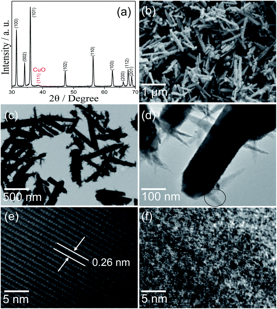
Fig. 1a represents the diffraction pattern of CuO/ZnO NRs. All the diffraction peaks in this pattern were found to match the ZnO phase (zincite), having a hexagonal geometry (JCPDS card no. 36-1451). The phases showed the major characteristic peaks with indices for crystalline ZnO. The peak corresponding to the base-centered monoclinic CuO (tenorite)-related secondary phase was also found at 2θ = 35.8° (100) (JCPDF card no. 073-6234). This indicates that there is a significant amount of crystalline CuO present in the nanomaterials. The morphology of CuO/ZnO NR heterostructures was examined by electron microscopy and the images obtained are displayed in Fig. 1b–f. The FESEM image reveals the formation of well-dispersed, nearly uniform ZnO NRs, as shown in Fig. 1b. The length and width of these ZnO NRs vary from 1.5 to 2.5 μm and from 100 to 200 nm, respectively. Deposition of CuO NPs results in the formation of spikes on the surface of ZnO NRs (Fig. 1b). These CuO NPs are uniformly distributed throughout the surface of ZnO NRs. More evidence on the deposition of CuO NPs on ZnO NRs was obtained by TEM, and the images obtained are shown in Fig. 1c and d. These images also confirm the formation of ZnO NRs having small CuO NPs on their surface. More interestingly, these small NPs are self-assembled in one direction and resulted in spike-like structure on the surface of ZnO NRs. The length and width of these spikes is 100 nm and 10 nm, respectively. The HRTEM image of ZnO NRs (Fig. 1e) clearly indicates the formation of a single crystalline structure with a lattice spacing of 0.26 nm, which indicates that these ZnO NRs grew along the c-axis. However, the HRTEM image of CuO spikes indicates its polycrystalline nature (Fig. 1f), which further proves that these spikes are composed of small NPs self-assembled in one direction.
 |
| | Fig. 1 (a) XRD profile and (b) FESEM image of CuO/ZnO NRs; TEM images of (c) CuO/ZnO NRs, (d) selected CuO/ZnO NRs; (e) HRTEM of ZnO and (f) HRTEM of CuO NPs. | |
Fig. 2 shows the XPS spectra of CuO/ZnO NRs. The binding energies of Cu 2p3/2, Zn 2p3/2, and O 1s were identified as 932.63, 1019.57, and 529.15 eV, respectively. The Cu 2p binding energies of the CuO/ZnO NRs were 932.63 (Cu 2p3/2) and 952.2 eV (Cu 2p1/2), which correspond to the binding energies of the Cu 2p of CuO.25 This indicates that Cu is in the +2 oxidation state. The peaks of Zn 2p3/2 and Zn 2p1/2 were observed at 1019.57 and 1042.76 eV, respectively, indicating that Zn is also in the +2 oxidation state (Fig. 2c). The peak of O 1s that appears in Fig. 2d indicates that O is from the CuO and ZnO. The peak centered at 529.15 eV (O1s) is associated to the O2− ion in the wurtzite structure. The shoulder peak at 531.04 eV is attributed to point defects or chemisorbed oxygen, possibly as OH, H2O or –CO3.26 The XPS measurements verify that the structures consist of CuO and ZnO.
 |
| | Fig. 2 XPS spectra of CuO/ZnO NRs; (a) survey, (b) Cu 2p, (c) Zn 2p and (d) O 1s. | |
In an aqueous solution of Cu2+ salt, positively charged metal ions are reduced by NaBH4 to form the uniform CuO NPs. In the present synthesis system, NaBH4 may act as both an alkaline reagent and reductant to control the growth of spike-like CuO architectures on ZnO NRs. The chemical reactions involved are believed to proceed as follows:27
| | |
BH4−(aq) + 4H2O → H3BO3(aq) + 4H2 + OH−(aq)
| (1) |
| | |
2Cu2+ +O2 + 2H2O + 4OH−(aq) → 2[Cu(OH)4]2−(aq)
| (2) |
| | |
8[Cu(OH)4]2−(aq) + BH4−(aq) → 4Cu2O(s) + H3BO3(aq) + 8H2O + 17OH−(aq)
| (3) |
| | |
2Cu2O(s) + O2 → 4CuO(s)
| (4) |
The growth model of our CuO/ZnO NRs is illustrated in Fig. 3. The initially generated CuO NPs are adsorbed on the ZnO NRs and provide nuclei for further growth. The CuO nuclei develop their own preferred growth pattern during the reaction process and form spike-like assemblies. Finally, the spike-like CuO nanostructures composed of numerous NPs are formed on ZnO NRs.
 |
| | Fig. 3 Schematic diagram of growth mechanism of CuO/ZnO NRs. | |
The resistance change of ZnO and CuO/ZnO NRs for 100–1000 ppm of CO gas is shown in Fig. 4a. The sensor resistance decreases with CO, and it reaches a near-saturation state in a few seconds; however, when the probe gas is stopped, the sensor resistance increases and reverts to the initial value. This shows that the response of CuO/ZnO NRs is higher than that of bare ZnO NRs. The maximum response of ZnO is 1.18 for 1000 ppm of CO, which increases to 5.58 with deposition of CuO NPs. It can be seen that response increases with increasing gas concentrations in both devices. For example, response of CuO/ZnO NRs increases from 2.77 to 5.58 with increasing CO concentration from 100 to 1000 ppm, respectively. It is important to note that the baseline resistance of ZnO NRs is relatively higher than that of CuO/ZnO NRs at every temperature, as displayed in Fig. 4b. Furthermore, baseline resistance increases with decreasing testing temperatures in both devices (Fig. 4b).
 |
| | Fig. 4 Variation of resistance of ZnO and CuO/ZnO NRs as a function of: (a) CO concentration at 300 °C. (b) Temperature in air. | |
The response of ZnO and CuO/ZnO NRs for 1000 ppm of CO at different temperatures was measured (Fig. 5a). The maximum response for ZnO NRs recorded at 400 °C is 4.18 for 1000 ppm of CO gas, which decreased to 1.03 at 250 °C. Functionalization of these ZnO NRs with CuO NPs further improved the response, especially at low working temperatures. For example, the response increases from 2.5 to 5.5 when the temperature is increased from 200 °C to 300 °C, respectively, which is higher than that from bare ZnO NRs at these temperatures. At 400 °C, the response of CuO/ZnO NRs (2.6) is slightly lower than that for ZnO (4.18). This suggests that the presence of CuO NPs increase the CO response at a lower temperature. The sensitivity of sensors made from CuO/ZnO NRs as a function of temperature and CO concentration is shown in Fig. 5b. As can be seen, the sensitivity increases with increasing CO concentration and temperature (except 400 °C). Interestingly, the sensitivity of CuO/ZnO NRs at 400 °C is even lower than that at 200 °C.
 |
| | Fig. 5 (a) Comparison of response of ZnO and CuO/ZnO NRs for 1000 ppm of CO at different temperatures and (b) CO sensitivity of CuO/ZnO NRs as a function of CO concentrations at different temperatures. | |
The gas-sensing mechanism of ZnO sensors involves the resistance change due to the chemical and electronic interaction between the gas and the ZnO. When a ZnO sensor is exposed to air, oxygen molecules adsorb on the surface of the materials to form O2−, O−, and O2− ions by capturing electrons from the conduction band. It is well known that O− is the stable oxygen ion that adsorbs on ZnO at 100–300 °C;28 therefore, it can be assumed that O− is the stable oxygen ion that adsorbs on ZnO at our testing temperatures.
When the sensor of ZnO is exposed to CO, the adsorbed CO gas then reacts with the chemisorbed oxygen anions on the surface, which can be described by the following reaction:
| | |
2CO(gas) + 2O(ads)− → 2CO2(gas) + 2e−
| (5) |
The gas removes the chemisorbed oxygen anions and is oxidized. The electrons produced cause a decrease in resistance of the ZnO. The decrease in baseline resistance with increasing temperatures is related to the increase of carrier concentration by thermal excitation of electrons from the valence band (VB) to the conduction band (CB). This electron mobility also increases with temperature, as transport of carriers among the grains is directly related to temperature. The temperature dependence of conductivity of a semiconductor can be approximated by eqn (6):29
| |
Rm = Rmo![[thin space (1/6-em)]](https://www.rsc.org/images/entities/char_2009.gif) exp(eVs/RT) exp(eVs/RT)
| (6) |
where, Vs is double potential energy barrier height,
RT is thermal energy, and
Rmo is resistance at Vs = 0; thus, resistance decreases with increasing temperature. However, the oxygen ion chemisorption process is also accelerated as the temperature is raised, and the potential energy barrier is also a function of atmosphere oxygen partial pressure:
30| |
 | (7) |
where
Nt is the surface density of adsorbed oxygen ions;
εr,
εo the permittivity of the semiconductor; and
Nd the volumetric density of the electron donors. The adsorption of oxygen molecules results in depletion-layer formation, which reduces the conductivity near the surface. However, baseline resistance decreases with increasing temperature, which suggests that electron concentration and transport is playing major role compared with oxygen ion chemisorption.
The sensing behavior of ZnO NRs after functionalization of CuO NPs is explained by both a collective- and local-site approach. In the collective-site approach, a tentative energy band diagram of CuO/ZnO NRs p–n heterojunction was constructed on the basis of available values regarding the band diagrams of ZnO and CuO (Fig. 6a). The band gap (Eg) of ZnO NRs is ∼3.4 eV, whereas the electron affinity (χ) of 4.35 eV was reported for ZnO.31,32 However, the value of the band gap of the CuO is a highly controversial issue, and different researchers have reported different values of the band gap with values ranging from 1.35 eV to 1.8 eV.33–35 Here, we applied the value of 1.35 eV for the band gap of CuO because it is the most reasonable and accepted value. Note that the electron affinity of CuO was reported to be 4.07 eV.33,34 From a thermodynamic point of view, the electrons transfer from CB of CuO to that of ZnO, while the holes immigrate in the opposite direction from VB of ZnO to that of CuO.35 This indicates the increased charge separation rate of electron–hole pairs under the bias potential and the longer lifetime of electron–hole pairs of CuO/ZnO NRs due to the formation of the p–n heterojunction. This longer lifetime of electron–hole pairs of CuO/ZnO NRs due to the formation of the p–n heterojunction may facilitate the adsorption of gas molecules. Thus, CuO/ZnO composite film shows higher sensing activity than that of pure ZnO film. However, formation of a p–n junction results in higher resistance; therefore, the resistance of CuO/ZnO should be higher compared with that of bare ZnO NRs. The lower baseline resistance of CuO/ZnO compared with bare ZnO is possibly related to the amount of CuO NP deposition.36 The electrical resistance of a bare ZnO NRs network can be represented as the series resistance of the ZnO NRs and the junction resistance formed between the NRs. In contrast, the resistance of a CuO/ZnO NR network can be represented as a series equivalent to that of ZnO NRs, p–n junction and CuO aggregates. Due to the presence of the p–n junction, the value of resistance of CuO/ZnO NRs is expected to be very high. However, at very high deposition levels, CuO can fully cover the ZnO-NWs network (Fig. S1, ESI†). Thus, a continuous CuO layer acts as a parallel resistance that reduces the total resistance of the sample (Fig. 6b). As a result, the resistance of CuO/ZnO NRs is lower than that of bare ZnO NRs.
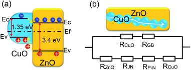 |
| | Fig. 6 Schematic diagram of (a) energy band diagram and (b) carrier transport in CuO/ZnO NRs. | |
In a local-site approach, a hard-soft acid–base interaction can be useful to explain the sensing behavior.37 It is well known that CO is a soft base; therefore, it prefers to interact with acidic centers like Cu2+ of CuO NPs. The improvement in response from CuO/ZnO NRs indicates that Cu2+ plays a very important role in adsorbing CO molecules in CO sensing.38 When CO molecules are adsorbed on the surface of the CuO NPs, they are preferably adsorbed and form bonds with the Cu2+ sites. The Cu–CO bonding consists of the donation of CO 5σ electrons to the metal, and the reverse donation of π-electrons from d orbitals of Cu to CO. In this way, the adsorption and reaction at the CuO–ZnO interface enhances the reaction of CO with the oxygen species and results in the enhancement of the CO reactivity, as observed in the CuO/ZnO NR sensor. Furthermore, the lower sensitivity of CuO/ZnO compared with that of ZnO at 400 °C (Fig. 5a) is possibly related to the agile and preferred oxidation of CO into CO2 on the surface of CuO NPs rather than by reaction with the adsorbed oxygen species on the ZnO surface.
Conclusions
In conclusion, ZnO NRs functionalized with CuO NPs were successfully synthesized by a simple chemical bath deposition. Single crystalline ZnO NRs having length and width 1–2.5 μm and 100–200 nm, respectively, were synthesized by a solvothermal method. Spike-like CuO NPs composed of small NPs (3–5 nm) self-assembled in one direction and uniformly deposited on the surface of ZnO NRs. The formation of p–n junctions improved the response due to increased lifetime of electron–hole pairs of CuO/ZnO NRs, which facilitated the adsorption of gas molecules. The increased response for CuO/ZnO NRs was further explained by the surface chemistry of CuO/ZnO NRs, which suggested that Cu in the +2 oxidation state preferentially adsorbs CO gas through Cu–CO bonding that consisted of the donation of CO 5σ electrons to the metal and the reverse donation of π-electrons from d orbitals of Cu to CO.
Acknowledgements
This paper was supported by (a) BK21 plus program from Ministry of Education and Human-Resource Development, (b) National Research Foundation (NRF) grant funded by the Korea government (MEST) (NRF-2010-0019626, 2012R1A2A010067873) and (c) Research Funds of Korea University in 2013.
Notes and references
- H.-R. Kim, A. Haensch, I.-D. Kim, N. Barsan, U. Weimar and J.-H. Lee, Adv. Funct. Mater., 2011, 21, 4456–4463 CrossRef CAS.
- Y. S. Kim, S. C. Ha, K. W. Kim, H. S. Yang, S. Y. Choi, Y. T. Kim, J. T. Park, C. H. Lee, J. Y. Choi, J. S. Park and K. Y. Lee, Appl. Phys. Lett., 2005, 86, 213105 CrossRef PubMed.
- C. C. Li, Z. F. Du, L. M. Li, H. C. Yu, Q. Wan and T. H. Wang, Appl. Phys. Lett., 2007, 91, 032101 CrossRef PubMed.
- S.-J. Kim, I.-S. Hwang, C. W. Na, I.-D. Kim, Y. C. Kang and J.-H. Lee, J. Mater. Chem., 2011, 21, 18560–18567 RSC.
- H. Y. Yu, B. H. Kang, U. H. Pi, C. W. Park, S. Y. Choi and G. T. Kim, Appl. Phys. Lett., 2007, 86, 253102 CrossRef PubMed.
- K.-M. Kim, H.-R. Kim, K.-I. Choi, H.-J. Kim and J.-H. Lee, Sens. Actuators, B, 2011, 155, 745–751 CrossRef CAS PubMed.
- Q. Qi, T. Zhang, L. Liu, X. Zheng, Q. Yu, Y. Zeng and H. Yang, Sens. Actuators, B, 2008, 134, 166–170 CrossRef CAS PubMed.
- V. Saxena, D. K. Aswal, M. Kaur, S. P. Koiry, S. K. Gupta, J. V. Yakhmi, R. J. Kshirsagar and S. K. Deshpande, Appl. Phys. Lett., 2007, 90, 043516 CrossRef PubMed.
- S. J. Chang, W. Y. Weng, C. L. Hsu and T. J. Hsueh, Nano Communication Networks, 2010, 1, 283–288 CrossRef PubMed.
- O. Lupana and G. Chai, Microelectron. Eng., 2008, 85, 2220–2225 CrossRef PubMed.
- P. Rai, Y.-S. Kim, H.-M. Song, M.-K. Song and Y.-T. Yu, Sens. Actuators, B, 2012, 165, 133–142 CrossRef CAS PubMed.
- M. Hübner, D. Koziej, J.-D. Grunwaldt, U. Weimar and N. Barsan, Phys. Chem. Chem. Phys., 2012, 14, 13249–13254 RSC.
- J. W. Shin, S.-J. Choi, I. Lee, D.-Y. Youn, C. O. Park, J.-H. Lee, H. L. Tuller and I.-D. Kim, Adv. Funct. Mater., 2013, 23, 2357–2367 CrossRef CAS.
- C. W. Na, H.-S. Woo and J.-H. Lee, RSC Adv., 2012, 2, 414–417 RSC.
- C. W. Na, H.-S. Woo, I.-D. Kim and J.-H. Lee, Chem. Commun., 2011, 47, 5148–5150 RSC.
- S.-J. Kim, C. W. Na, I.-S. Hwang and J.-H. Lee, Sens. Actuators, B, 2012, 168, 83–89 CrossRef CAS PubMed.
- M. Mashock, K. Yu, S. Cui, S. Mao, G. Lu and J. Chen, ACS Appl. Mater. Interfaces, 2012, 4, 4192–4199 CAS.
- Y. Nakamura, H. Yoshioka, M. Miyayama, H. Yanagida, T. Tsurutani and Y. Nakamura, J. Electrochem. Soc., 1990, 137, 940–943 CrossRef CAS PubMed.
- S. J. Jung and H. Yanagida, Sens. Actuators, B, 1996, 37, 55–60 CrossRef CAS.
- J. Kim, W. Kim and K. Yong, J. Phys. Chem. C, 2012, 116, 15682–15691 CAS.
- J. X. Wang, X. W. Sun, Y. Yang, K. K. A. Kyaw, X. Y. Huang, J. Z. Yin, J. Wei and H. V. Demir, Nanotechnology, 2011, 22, 325704 CrossRef CAS PubMed.
- P. Rai and Y.-T. Yu, Sens. Actuators, B, 2012, 161, 748–754 CrossRef CAS PubMed.
- P. Rai, W.-K. Kwak and Y.-T. Yu, ACS Appl. Mater. Interfaces, 2013, 5, 3026–3032 CAS.
- E. Sendzikiene, V. Makareviciene and P. Janulis, Renewable Energy, 2006, 31, 2505–2512 CrossRef CAS PubMed.
- J. Kim, W. Kim and K. Yong, J. Phys. Chem. C, 2012, 116, 15682–15691 CAS.
- D. Deng, S. T. Martin and S. Ramanathan, Nanoscale, 2010, 2, 2685–2691 RSC.
- G. Fan and F. Li, Chem. Eng. J., 2011, 167, 388–396 CrossRef CAS PubMed.
- M. Takata, D. Tsubone and H. Yanagida, J. Am. Ceram. Soc., 1976, 59, 4–8 CrossRef CAS PubMed.
- N. Yamazoe, K. Shimanoe and C. Sawada, Thin Solid Films, 2007, 515, 8302–8309 CrossRef CAS PubMed.
- G. Zhang and M. Liu, Sens. Actuators, B, 2000, 69, 144–152 CrossRef CAS.
- P. S. Nayar, J. Appl. Phys., 1982, 53, 1069 CrossRef CAS PubMed.
- Z. Guo, D. X. Zhao, Y. C. Liu, D. Z. Shen, J. Y. Zhang and B. H. Li, Appl. Phys. Lett., 2008, 93, 163501 CrossRef PubMed.
- F. P. Koffyberg and F. A. Benko, J. Appl. Phys., 1982, 53, 1173 CrossRef CAS PubMed.
- M. T. S. Nair, L. Guerrero, O. L. Arenas and P. K. Nair, Appl. Surf. Sci., 1999, 150, 143–151 CrossRef CAS.
- R. V. Pisarev, V. V. Pavlov, A. M. Kalashnikova and A. S. Moskvin, Phys. Rev. B: Condens. Matter Mater. Phys., 2010, 82, 224502 CrossRef.
- N. Datta, N. Ramgir, M. Kaur, S. K. Ganapathi, A. K. Debnath, D. K. Aswal and S. K. Gupta, Sens. Actuators, B, 2012, 166–167, 394–401 CrossRef CAS PubMed.
- R. G. Pearson, Coord. Chem. Rev., 1990, 100, 403–425 CrossRef CAS.
- L. Liao, Z. Zhang, B. Yan, Z. Zheng, Q. L. Bao, T. Wu, C. M. Li, Z. X. Shen, J. X. Zhang, H. Gong, J. C. Li and T. Yu, Nanotechnology, 2009, 20, 085203 CrossRef CAS PubMed.
Footnote |
| † Electronic supplementary information (ESI) available: FESEM images of CuO/ZnO NRs. See DOI: 10.1039/c4ra00078a |
|
| This journal is © The Royal Society of Chemistry 2014 |
Click here to see how this site uses Cookies. View our privacy policy here.